
Features
l Easy to handle since there are no wires on chip
(AnSn eutectic bonding)
Optical fibers can be brought closer to the chip
l Miniature package: 2 ◊ 2 ◊ 1 mm
l High sensitivity: 0.95 A/W Typ. (=1.55 µm)
l Precise chip position tolerance: ±0.075 mm
Applications
l LD monitor
l Optical fiber communication
P H O T O D I O D E
InGaAs PIN photodiode
Uses small package with no wire
G9230-01
PRELIMINARY DATA
Jan. 2003
1
I General / Absolute maximum ratings
Parameter
Symbol
value
Unit
Active area
-
f0.3
mm
Reverse voltage
V
R
Max.
10
V
Operating temperature *
Topr.
-40 to +85
∞C
Storage temperature *
Tstg.
-40 to +85
∞C
* In N
environment or in vacuum
I Electrical and optical characteristics (Ta=25 ∞C)
Parameter
Symbol
Condition
Min.
Typ.
Max.
Unit
Spectral response range
l
-
0.95 to 1.7
-
µm
l=1.3 µm
-
0.85
-
A/W
Photo sensitivity
S
l=1.55 µm
0.85
0.95
-
A/W
Dark current
I
D
V
R
=5 V
-
0.3
1.5
nA
Shunt resistance
Rsh
V
R
=10 mV
-
1000
-
MW
Terminal capacitance
Ct
V
R
=5 V, f=1 MHz
-
5
-
pF
Cut-off frequency
fc
V
R
=5 V, R
L
=50 W
-
400
-
MHz
Noise equivalent power
NEP
l=lp-
4 ◊ 10
-15
-
W/Hz
1/2
InGaAs PIN photodiode
G9230-01
HAMAMATSU PHOTONICS K.K., Solid State Division
1126-1 Ichino-cho, Hamamatsu City, 435-8558 Japan, Telephone: (81) 053-434-3311, Fax: (81) 053-434-5184, http://www.hamamatsu.com
U.S.A.: Hamamatsu Corporation: 360 Foothill Road, P.O.Box 6910, Bridgewater, N.J. 08807-0910, U.S.A., Telephone: (1) 908-231-0960, Fax: (1) 908-231-1218
Germany: Hamamatsu Photonics Deutschland GmbH: Arzbergerstr. 10, D-82211 Herrsching am Ammersee, Germany, Telephone: (49) 08152-3750, Fax: (49) 08152-2658
France: Hamamatsu Photonics France S.A.R.L.: 8, Rue du Saule Trapu, Parc du Moulin de Massy, 91882 Massy Cedex, France, Telephone: 33-(1) 69 53 71 00, Fax: 33-(1) 69 53 71 10
United Kingdom: Hamamatsu Photonics UK Limited: 2 Howard Court, 10 Tewin Road, Welwyn Garden City, Hertfordshire AL7 1BW, United Kingdom, Telephone: (44) 1707-294888, Fax: (44) 1707-325777
North Europe: Hamamatsu Photonics Norden AB: Smidesv‰gen 12, SE-171 41 Solna, Sweden, Telephone: (46) 8-509-031-00, Fax: (46) 8-509-031-01
Italy: Hamamatsu Photonics Italia S.R.L.: Strada della Moia, 1/E, 20020 Arese, (Milano), Italy, Telephone: (39) 02-935-81-733, Fax: (39) 02-935-81-741
Information furnished by HAMAMATSU is believed to be reliable. However, no responsibility is assumed for possible inaccuracies or omissions.
Specifications are subject to change without notice. No patent rights are granted to any of the circuits described herein. ©2003 Hamamatsu Photonics K.K.
Cat. No. KIRD1055E02
Apr. 2003 DN
1.0
1.0
0.2
ANODE
CATHODE
Tolerance unless otherwise noted: ±0.075
Values in parentheses indicate reference value.
ACTIVE AREA
0.3
0.6
2.0
2.0
0.2
(0.6)
(0.5)
(0.5)
(0.2)
(Typ. Ta=25 ∞C)
0.8
1
1.4
1.6
1.8
WAVELENGTH (µm)
PHOTO SENSITIVITY (A/W)
1.0
0.8
0.6
0.4
0.2
0
1.2
1.2
KIRDA0168EA
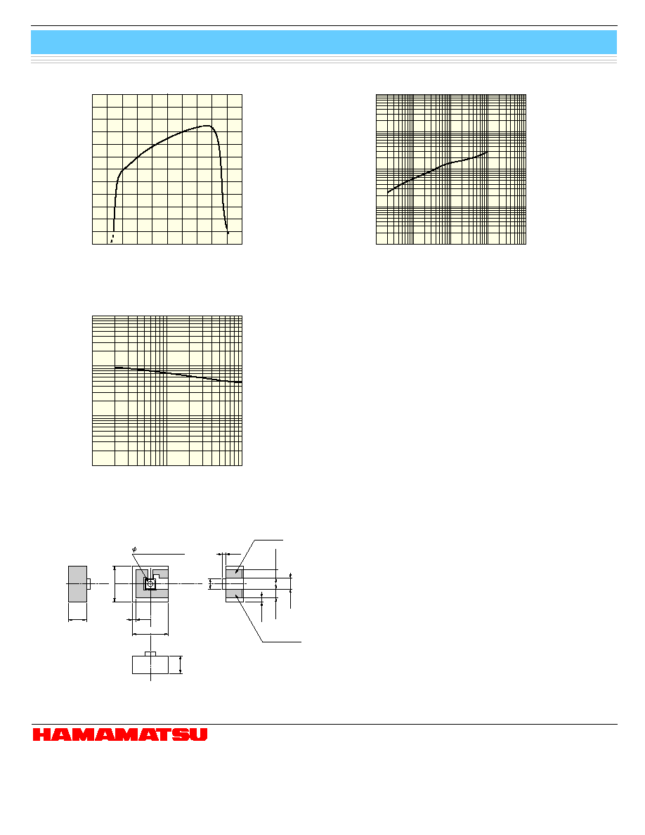
I Dimensional outline (unit: mm)
I Spectral response
I Dark current vs. reverse voltage
I Terminal capacitance vs. reverse voltage
KIRDB0287EA
2
(Typ. Ta=25 ∞C)
0.01
0.1
10
100
REVERSE VOLTAGE (V)
DARK CURRENT
1 pA
10 nA
1 nA
100 pA
10 pA
1
KIRDB0288EA
(Typ. Ta=25 ∞C, f=1 MHz)
0.1
10
REVERSE VOLTAGE (V)
TERMINAL CAPACITANCE (pF)
0.1
100
10
1
1
KIRDB0289EA