 | –≠–ª–µ–∫—Ç—Ä–æ–Ω–Ω—ã–π –∫–æ–º–ø–æ–Ω–µ–Ω—Ç: 2SK973 | –°–∫–∞—á–∞—Ç—å:  PDF PDF  ZIP ZIP |
Application
High speed power switching
Features
∑ Low on-resistance
∑ High speed switching
∑ Low drive current
∑ 4 V gate drive device
≠ Can be driven from 5 V source
∑ Suitable for motor drive, DC-DC converter,
power switch and solenoid drive
Table 1 Absolute Maximum Ratings (Ta = 25∞C)
Item
Symbol
Ratings
Unit
--------------------------------------------------------------------------------------
Drain to source voltage
V
DSS
60
V
--------------------------------------------------------------------------------------
Gate to source voltage
V
GSS
±20
V
--------------------------------------------------------------------------------------
Drain current
I
D
2
A
--------------------------------------------------------------------------------------
Drain peak current
I
D(peak)
*
8
A
--------------------------------------------------------------------------------------
Body to drain diode reverse drain current
I
DR
2
A
--------------------------------------------------------------------------------------
Channel dissipation
Pch**
10
W
--------------------------------------------------------------------------------------
Channel temperature
Tch
150
∞C
--------------------------------------------------------------------------------------
Storage temperature
Tstg
≠55 to +150
∞C
--------------------------------------------------------------------------------------
*
PW
10 µs, duty cycle
1 %
**
Value at T
C
= 25 ∞C
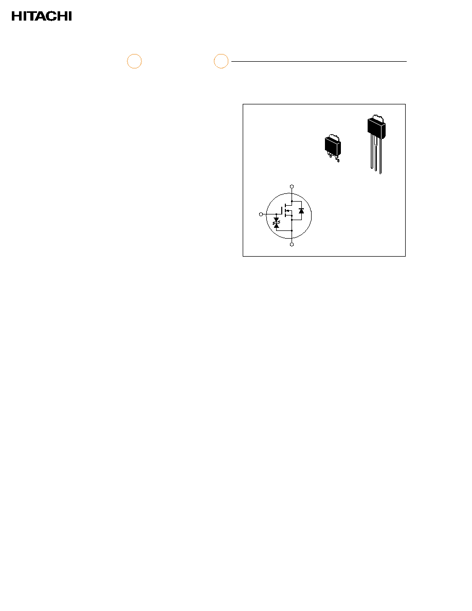
2SK973
L
, 2SK973
S
Silicon N-Channel MOS FET
1
2
3
4
2, 4
1
3
DPAK-1
S type
L type
1. Gate
2. Drain
3. Source
4. Drain
1
2
3
4

Table 2 Electrical Characteristics (Ta = 25∞C)
Item
Symbol
Min
Typ
Max
Unit
Test conditions
--------------------------------------------------------------------------------------
Drain to source breakdown
V
(BR)DSS
60
--
--
V
I
D
= 10 mA, V
GS
= 0
voltage
--------------------------------------------------------------------------------------
Gate to source breakdown
V
(BR)GSS
±20
--
--
V
I
G
= ±100 µA, V
DS
= 0
voltage
--------------------------------------------------------------------------------------
Gate to source leak current
I
GSS
--
--
±10
µA
V
GS
= ±16 V, V
DS
= 0
--------------------------------------------------------------------------------------
Zero gate voltage drain current
I
DSS
--
--
100
µA
V
DS
= 50 V, V
GS
= 0
--------------------------------------------------------------------------------------
Gate to source cutoff voltage
V
GS(off)
1.0
--
2.0
V
I
D
= 1 mA, V
DS
= 10 V
--------------------------------------------------------------------------------------
Static drain to source on state
R
DS(on)
--
0.25
0.35
I
D
= 1 A, V
GS
= 10 V *
resistance
--------------
--------------------≠
0.40
0.50
I
D
= 1 A, V
GS
= 4 V *
--------------------------------------------------------------------------------------
Forward transfer admittance
|y
fs
|
1.2
2.0
--
S
I
D
= 1 A, V
DS
= 10 V *
--------------------------------------------------------------------------------------
Input capacitance
Ciss
--
240
--
pF
V
DS
= 10 V, V
GS
= 0,
----------------------------------------------------------------
Output capacitance
Coss
--
115
--
pF
f = 1 MHz
----------------------------------------------------------------
Reverse transfer capacitance
Crss
--
35
--
pF
--------------------------------------------------------------------------------------
Turn-on delay time
t
d(on)
--
4
--
ns
I
D
= 1 A, V
GS
= 10 V,
----------------------------------------------------------------
Rise time
t
r
--
15
--
ns
R
L
= 30
----------------------------------------------------------------
Turn-off delay time
t
d(off)
--
80
--
ns
----------------------------------------------------------------
Fall time
t
f
--
40
--
ns
--------------------------------------------------------------------------------------
Body to drain diode forward
V
DF
--
1.0
--
V
I
F
= 2 A, V
GS
= 0
voltage
--------------------------------------------------------------------------------------
Body to drain diode reverse
t
rr
--
70
--
ns
I
F
= 2 A, V
GS
= 0,
recovery time
di
F
/dt = 50 A/µs
--------------------------------------------------------------------------------------
* Pulse Test
2SK973 L , 2SK973 S

50
100
0
Case Temperature T
C
(∞C)
150
5
Channel Dissipation Pch
(W)
10
15
Power vs. Temperature Derating
Maximum Safe Operation Area
Drain Current I
D
(A)
0.3
1.0
3
1.0
3
10
10
30
50
Drain to Source Voltage V
DS
(V)
0.1
100
0.3
30
0.05
0.1
100
µ
s
1 ms
PW = 10 ms (1 Shot)
DC Operation (T
C
= 25∞C)
Ta = 25∞C
10
µ
s
Operation in this area is
limited by R
DS (on)
Typical Output Characteristics
6
Drain to Source Voltage V
DS
(V)
8
4
2 10
Drain Current I
D
(A)
0
1
2
3
4
0
5
V
GS
= 2 V
Pulse Test
10 V
5 V
4 V
3 V
3.5 V
2.5 V
Typical Transfer Characteristics
3
Gate to Source Voltage V
GS
(V)
4
2
1
0
5
1
2
3
4
5
0
Drain Current I
D
(A)
T
C
= 25∞C
75∞C
V
DS
= 10 V
Pulse Test
≠25∞C
2SK973 L , 2SK973 S
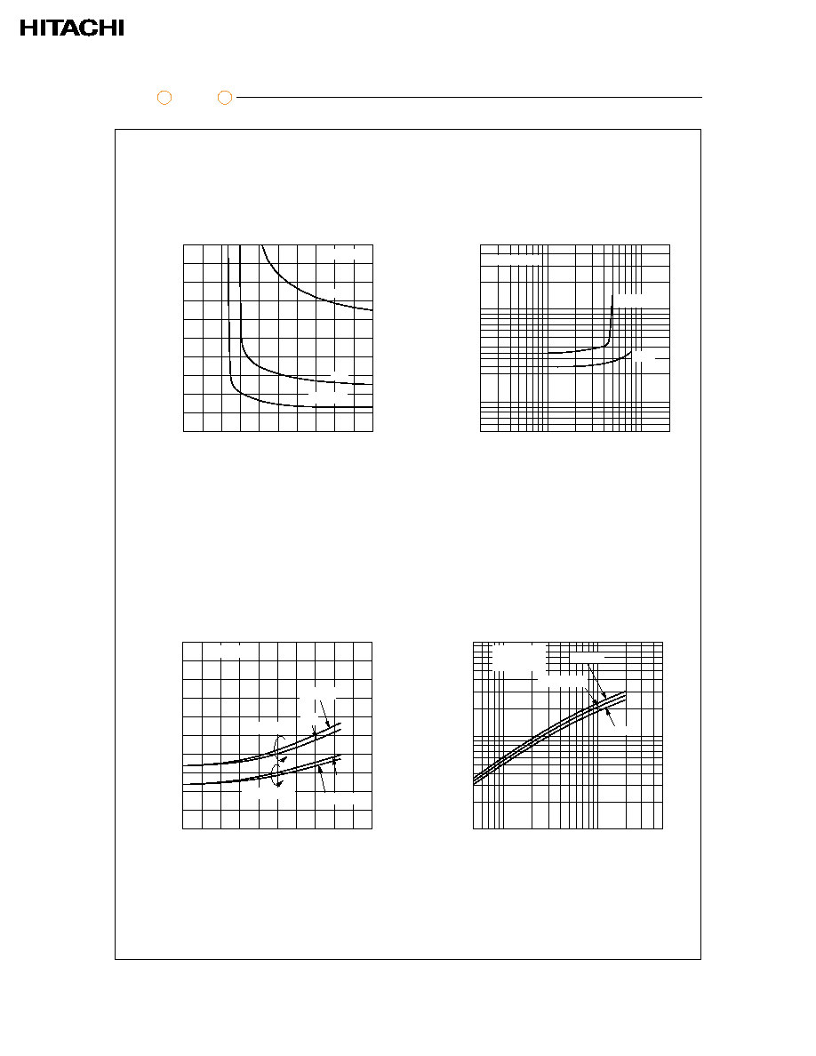
Drain to Source Saturation Voltage
vs. Gate to Source Voltage
6
Gate to Source Voltage V
GS
(V)
8
4
2
0
10
0.8
1.2
1.6
2.0
0
0.4
Drain to Source Saturation Voltage
V
DS (on)
(V)
Pulse Test
I
D
= 1 A
5 A
2 A
2
Drain Current I
D
(A)
5
1.0
0.5
20
0.2
0.5
1.0
2
5
0.2
0.1
0.05
10
Static Drain to Source on State
Resistance vs. Drain Current
Static Drain to Source on State Resistance
R
DS (on)
(
)
V
GS
= 4 V
10 V
Pulse Test
80
Case Temperature T
C
(∞C)
120
40
0
0.2
0.4
0.6
0.8
1.0
≠40
0
160
Static Drain to Source on State
Resistance vs. Temperature
Static Drain to Source on State Resistance
R
DS (on)
(
)
I
D
= 2 A
Pulse Test
V
GS
= 4 V
V
GS
= 10 V
5 A
1 A
1 A, 2 A
Forward Transfer Admittance
vs. Drain Current
10
5
2
1.0
0.5
0.2
0.1
0.05
0.1
0.2
0.5
1.0
5
Drain Current I
D
(A)
2
Forward Transfer Admittance
yfs
(S)
T
C
= 25∞C
V
DS
= 10 V
Pulse Test
≠25∞C
75∞C
2SK973 L , 2SK973 S
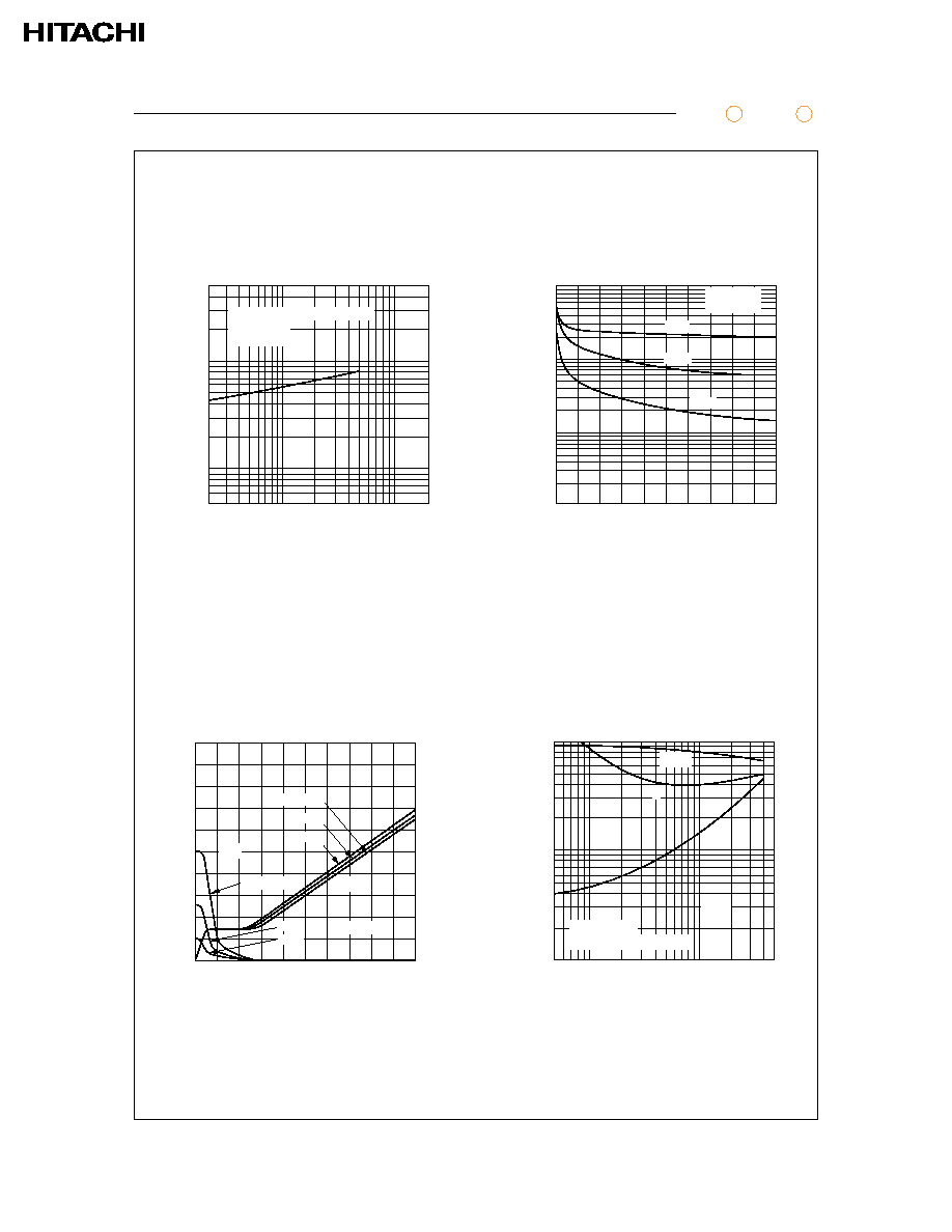
500
200
100
50
20
10
5
0.2
0.5
2
20
Reverse Drain Current I
DR
(A)
5
1.0
10
Body to Drain Diode Reverse
Recovery Time
Reverse Recovery Time t
rr
(ns)
di/dt = 50 A/
µ
s, Ta = 25∞C
V
GS
= 0
Pulse Test
Typical Capacitance vs.
Drain to Source Voltage
1000
300
100
30
3
1
Capacitance C (pF)
0
10
20
50
Drain to Source Voltage V
DS
(V)
30
10
40
V
GS
= 0
f = 1 MHz
Ciss
Coss
Crss
100
80
60
40
20
0
2
6
8
Gate Charge Qg (nc)
4
20
16
12
8
4
Dynamic Input Characteristics
Drain to Source Voltage V
DS
(V)
Gate to Source Voltage V
GS
(V)
10
V
DS
V
GS
V
DD
= 50 V
10 V
25 V
V
DD
= 50 V
25 V
10 V
I
D
= 2 A
0
Switching Characteristics
100
50
20
10
2
1
0.05
0.1
0.5
5
Drain Current I
D
(A)
1.0
0.2
2
Switching Time t (ns)
5
t
d (off)
t
f
t
r
V
GS
= 10 V
PW = 2
µ
s, duty < 1 %
t
d (on)
2SK973 L , 2SK973 S

2SK973 L , 2SK973 S
3
1.0
0.3
0.1
0.03
0.01
10
µ
1 m
10 m
100 m
Pulse Width PW (s)
100
µ
1
10
Normalized Transient Thermal Impedance vs. Pulse Width
Normalized Transient Thermal Impedance
S
(t)
ch≠c(t) =
S
(t) ∑
ch≠c
ch≠c = 12.5∞C/W, T
C
= 25∞C
P
DM
PW
D = PW
T
T
T
C
= 25∞C
D = 1
0.5
0.05
1 Shot Pulse
0.2
0.1
0.02
0.01
5
4
3
2
1
0
0.4
1.2
1.6
2.0
Source to Drain Voltage V
SD
(V)
0.8
Reverse Drain Current vs.
Source to Drain Voltage
Reverse Drain Current I
DR
(A)
V
GS
= 0, ≠5 V
Pulse Test
10 V
15 V
5 V

2SK973 L , 2SK973 S
Vin Monitor
Vout Monitor
R
L
50
Vin = 10 V
D.U.T
.
V
DD
= 30 V
.
Switching Time Test Circuit
Vin
10 %
90 %
90 %
90 %
10 %
td (on)
td (off)
tr
tf
Vout
10 %
Wavewforms