
HD151TS301RP
Clock Generator for Printer
ADE-205-603D (Z)
Rev. 4
Sep. 2001
Description
The HD151TS301RP is a high-performance clock generator. It is specifically designed for printer.
Features
∑
Supports 20 MHz to 50 MHz operation. (Designed for 24 MHz and 48 MHz)
∑
1 copy of clock out with spread spectrum modulation @3.3 V
∑
1 copy of reference clock @3.3 V
∑
Programmable spread spectrum modulation (≠0.5%, ≠1.0%, ≠2.0% and ≠3.0% down spread
modulation.)
∑
SOP-8pin
Key Specifications
∑
Supply voltages : VDD = 3.3 V±0.165 V
∑
Ta = 0 to 70∞C operating range
∑
Clock output duty cycle = 50±5%

HD151TS301RP
Rev.4, Sep. 2001, page 2 of 8
Pin Arrangement
(Top view)
8
SEL1
1
7
CLKOUT
6
SEL0
5
XOUT
SSCCLKOUT
2
VDD
3
GND
4
XIN
SSC Function Table
SEL1 :0
Spread Percentage
0 0
≠1.0%
0 1
≠3.0%
1 0
≠2.0%
1 1
≠0.5%
Note:
≠3.0% spread percentage is selected @ default.
HD151TS301RP
Rev.4, Sep. 2001, page 3 of 8
Pin Descriptions
Pin name
No.
Type
Description
GND
3
Ground
GND pins
VDD
2
Power
Power supplies pins. Nominal 3.3 V.
CLKOUT
7
Output
Normal 3.3 V reference clock output.
SSCCLKOUT
1
Output
Spread spectrum modulated clock output.
XIN
4
Input
Oscillator input.
XOUT
5
Output
Oscillator output.
SEL0
6
Input
SSC mode select pin. LVCMOS level input.
Internal pull≠up resistors (typically 100 k
).
SEL1
8
Input
SSC mode select pin. LVCMOS level input.
Internal pull≠down resistors (typically 100 k
).
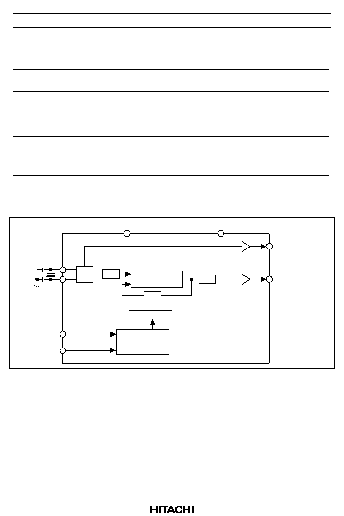
Block Diagram
Synthesizer
Mode Control
1/n
OSC
SSC Modulator
VDD
CLKOUT
SSCCLKOUT
GND
1/2
SEL0
XIN
XOUT
SEL1
1/m

HD151TS301RP
Rev.4, Sep. 2001, page 4 of 8
Absolute Maximum Ratings
Item
Symbol
Ratings
Unit
Conditions
Supply voltage
VDD
≠0.5 to 4.6
V
Input voltage
V
I
≠0.5 to 4.6
V
Output voltage
*1
V
O
≠0.5 to
VDD+0.5
V
Input clamp current
I
IK
≠50
mA
V
I
< 0
Output clamp current
I
OK
≠50
mA
V
O
< 0
Continuous output current
I
O
±50
mA
V
O
= 0 to VDD
Maximum power dissipation
at Ta = 55∞C (in still air)
0.7
W
Storage temperature
T
stg
≠65 to +150
∞C
Notes:
Stresses beyond those listed under "absolute maximum ratings" may cause permanent damage
to the device. These are stress ratings only, and functional operation of the device at these or
any other conditions beyond those indicated under "recommended operating conditions" is not
implied. Exposure to absolute maximum rated conditions for extended periods may affect device
reliability.
1. The input and output negative voltage ratings may be exceeded if the input and output clamp
current ratings are observed.
Recommended Operating Conditions
Item
Symbol
Min
Typ
Max
Unit Conditions
Supply voltage
VDD
3.135
3.3
3.465
V
DC input signal voltage
≠0.3
--
VDD+0.3
V
High level input voltage
V
IH
2.0
--
VDD+0.3
V
Low level input voltage
V
IL
≠0.3
--
0.8
V
Operating temperature
T
a
0
--
70
∞C
Input clock duty cycle
45
50
55
%

HD151TS301RP
Rev.4, Sep. 2001, page 5 of 8
DC Electrical Characteristics
Ta = 0 to 70∞C, VDD = 3.3 V±5%
Item
Symbol
Min
Typ
Max
Unit
Test Conditions
Input low voltage
V
IL
--
--
0.8
V
Input high voltage
V
IH
2.0
--
--
V
Input current
I
I
--
--
±10
µA
V
I
= 0 V or 3.465 V,
VDD = 3.465 V, XIN
--
--
±100
V
I
= 0 V or 3.465 V,
VDD = 3.465 V, SEL0, SEL1
Input slew rate
SR
1
--
4
V / ns 20% ≠ 80%
Input capacitance
C
I
--
--
4
pF
SEL0, SEL1
Operating current
--
11
--
mA
XIN = 24 MHz, C
L
= 0 pF,
VDD = 3.3 V
--
22
--
XIN = 48 MHz, C
L
= 0 pF,
VDD = 3.3 V
DC Electrical Characteristics / Clock Output & SSC Clock Output
Ta = 0 to 70∞C, VDD = 3.3 V±5%
Item
Symbol
Min
Typ
Max
Unit
Test Conditions
Output voltage
V
OH
3.1
--
--
V
I
OH
= ≠1 mA, VDD = 3.3 V
V
OL
--
--
50
mV
I
OL
= 1 mA, VDD = 3.3 V
Output current
I
OH
≠55
≠85
≠125
mA
V
OH
= 1.5 V
I
OL
55
75
105
V
OL
= 1.5 V