 | –≠–ª–µ–∫—Ç—Ä–æ–Ω–Ω—ã–π –∫–æ–º–ø–æ–Ω–µ–Ω—Ç: HD74AC174 | –°–∫–∞—á–∞—Ç—å:  PDF PDF  ZIP ZIP |

HD74AC174
Hex D-Type Flip-Flop with Master Reset
Description
The HD74AC174 is a high-speed hex D flip-flop. The device is used primarily as a 6-bit edge-triggered
storage register. The information on the D inputs is transferred to storage during the Low-to-High clock
transition. The device has a Master Reset to simultaneously clear all flip-flops.
Feature
∑
Outputs Source/Sink 24 mA
Pin Arrangement
1
2
3
4
5
6
7
8
16
15
14
13
12
11
10
9
MR
Q
0
D
0
D
1
Q
1
Q
2
D
2
GND
V
CC
Q
5
D
5
D
4
Q
4
D
3
Q
3
CP
(Top view)

HD74AC174
2
Logic Symbol
D
0
D
1
D
2
D
3
D
4
D
5
Q
0
CP
MR
Q
1
Q
2
Q
3
Q
4
Q
5
Pin Names
D
0
to D
5
Data Inputs
CP
Clock Pulse Input
MR
Master Reset Input
Q
0
to Q
5
Outputs
Functional Description
The HD74AC174 consists of six edge-triggered D flip-flops with individual D inputs and Q outputs. The
Clock (CP) and Master Reset (
MR) are common to all flip-flops. Each D input's state is transferred to the
corresponding flip-flops's output following the Low-to-High Clock (CP) transition. A Low input to the
Master Reset (
MR) will force all outputs Low independent of Clock or Data inputs. The HD74AC174 is
useful for applications where the true output only is required and the Clock and Master Reset are common
to all storage elements.
Truth Table
Inputs
Output
MR
CP
D
Q
L
X
X
L
H
H
H
H
L
L
H
L
X
Q
H :
High Voltage Level
L
:
Low Voltage Level
X :
Immaterial
: Low-to-High Transition of Clock
HD74AC174
3
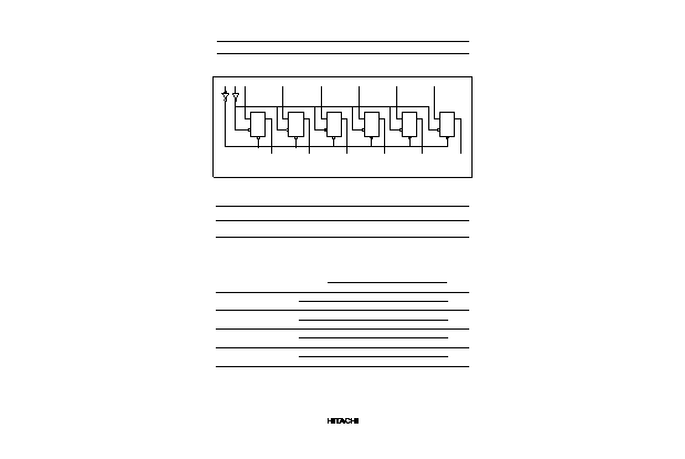
Logic Diagram
CP
CD
CP
MR
D
5
Q
5
Q
4
Q
3
Q
2
Q
1
Q
0
D
4
D
3
D
2
D
1
D
0
D
Q
CP
CD
D
Q
CP
CD
D
Q
CP
CD
D
Q
CP
CD
D
Q
CP
CD
D
Q
Please note that this diagram is provided only for the understanding of logic operations and should not be
used to estimate propagation delays.
DC Characteristics (unless otherwise specified)
Item
Symbol
Max
Unit
Condition
Maximum quiescent supply current
I
CC
80
µ
A
V
IN
= V
CC
or ground, V
CC
= 5.5 V,
Ta = Worst case
Maximum quiescent supply current
I
CC
8.0
µ
A
V
IN
= V
CC
or ground, V
CC
= 5.5 V,
Ta = 25
∞
C
AC Characteristics: HD74AC174
Ta = +25
∞
C
C
L
= 50 pF
Ta = ≠40
∞
C to +85
∞
C
C
L
= 50 pF
Item
Symbol
V
CC
(V)*
1
Min
Typ
Max
Min
Max
Unit
Maximum clock
f
max
3.3
90
100
--
70
--
MHz
frequency
5.0
100
125
--
100
--
Propagation delay
t
PLH
3.3
1.0
9.0
11.5
1.0
12.5
ns
CP to Q
n
5.0
1.0
6.0
8.5
1.0
9.5
Propagation delay
t
PHL
3.3
1.0
8.5
11.0
1.0
12.0
ns
CP to Q
n
5.0
1.0
6.0
8.0
1.0
9.0
Propagation delay
t
PHL
3.3
1.0
9.0
11.5
1.0
12.5
ns
MR
to Q
n
5.0
1.0
7.0
9.0
1.0
10.5
Note:
1. Voltage Range 3.3 is 3.3 V
±
0.3 V
Voltage Range 5.0 is 5.0 V
±
0.5 V
HD74AC174
4
AC Operating Requirements: HD74AC174
Ta = +25
∞
C
C
L
= 50 pF
Ta = ≠40
∞
C
to +85
∞
C
C
L
= 50 pF
Item
Symbol
V
CC
(V)*
1
Typ
Guaranteed Minimum
Unit
Setup time, HIGH or LOW
t
su
3.3
2.5
6.5
7.0
ns
D
n
to CP
5.0
2.0
5.0
5.5
Hold time, HIGH or LOW
t
h
3.3
1.0
3.0
3.0
ns
D
n
to CP
5.0
0.5
3.0
3.0
MR
pulse width, LOW
t
w
3.3
1.0
5.5
7.0
ns
5.0
1.0
5.0
5.0
CP pulse width
t
w
3.3
1.0
5.5
7.0
ns
5.0
1.0
5.0
5.0
Recovery time
t
rec
3.3
0
2.5
2.5
ns
MR
to CP
5.0
0
2.0
2.0
Note:
1. Voltage Range 3.3 is 3.3 V
±
0.3 V
Voltage Range 5.0 is 5.0 V
±
0.5 V
Capacitance
Item
Symbol
Typ
Unit
Condition
Input capacitance
C
IN
4.5
pF
V
CC
= 5.5 V
Power dissipation capacitance
C
PD
85.0
pF
V
CC
= 5.0 V

Hitachi Code
JEDEC
EIAJ
Weight (reference value)
DP-16
Conforms
Conforms
1.07 g
Unit: mm
6.30
19.20
16
9
8
1
1.3
20.00 Max
7.40 Max
7.62
0.25
+ 0.13
≠ 0.05
2.54
±
0.25
0.48
±
0.10
0.51 Min
2.54 Min
5.06 Max
0
∞
≠ 15
∞
1.11 Max