Äîêóìåíòàöèÿ è îïèñàíèÿ www.docs.chipfind.ru

HD74LV221A
Dual Monostable Multivibrators
ADE-205-271A (Z)
2nd Edition
June 1999
Description
The HD74LV221A features output pulse-duration control by three methods. In the first method, the A
input is low and the B input goes high. In the second method, the B input is high and the
A input goes low.
In the third method, the
A input is low, the B input is high, and the clear (CLR) input goes high.
The basic pulse duration is programmed by selecting external resistance and capacitance values. The
external timing capacitor must be connected between Cext and Rext/Cext (positive) and an external resistor
connected between Rext/Cext and V
CC
.
To obtain variable pulse durations, connect an external variable resistance between Rext/Cext and VCC.
Pulse duration can be reduced by taking
CLR low.
Features
·
V
CC
= 2.0 V to 5.5 V operation
·
All inputs V
IH
(Max.) = 5.5 V (@V
CC
= 0 V to 5.5 V)
·
All outputs V
O
(Max.) = 5.5 V (@V
CC
= 0 V)
·
Output current
±
6 mA (@V
CC
= 3.0 V to 3.6 V),
±
12 mA (@V
CC
= 4.5 V to 5.5 V)
HD74LV221A
2
Function Table
Inputs
Outputs
CLR
A
B
Q
Q
L
X
X
L
H
X
H
X
L
H
X
X
L
L
H
H
L
H
H
L
H
Note:
H:
High level
L:
Low level
X:
Immaterial
:
Low to high transition
:
High to low transition
:
High level pulse
: Low level pulse
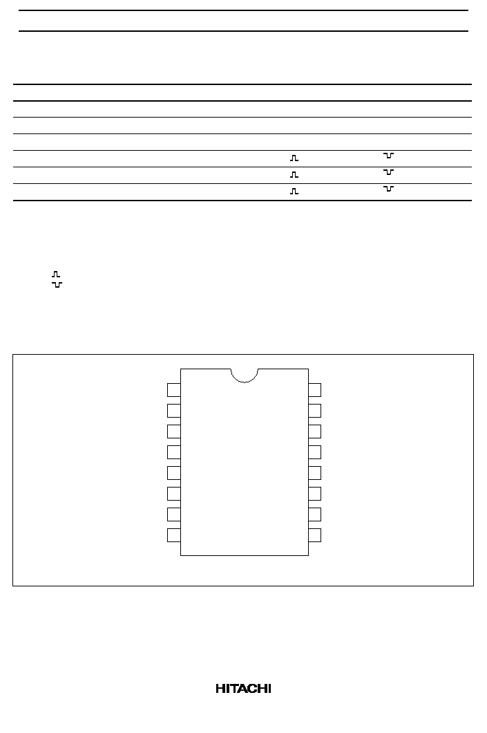
Pin Arrangement
V
CC
1Rext / Cext
1Cext
1Q
2B
2
Q
2
CLR
1
A
1B
1
CLR
1
Q
2Q
2Cext
2Rext / Cext
2
A
(Top view)
11
12
13
14
15
16
1
2
3
4
5
6
7
GND 8
9
10
HD74LV221A
3
Absolute Maximum Ratings
Item
Symbol
Ratings
Unit
Conditions
Supply voltage range
V
CC
0.5 to 7.0
V
Input voltage range*
1
V
I
0.5 to 7.0
V
Output voltage range*
1, 2
V
O
0.5 to V
CC
+ 0.5
V
Output: H or L
0.5 to 7.0
V
CC
: OFF
Input clamp current
I
IK
20
mA
V
I
< 0
Output clamp current
I
OK
±
50
mA
V
O
< 0 or V
O
> V
CC
Continuous output current
I
O
±
25
mA
V
O
= 0 to V
CC
Continuous current through
V
CC
or GND
I
CC
or I
GND
±
50
mA
Maximum power dissipation
at Ta = 25
°
C (in still air)*
3
P
T
785
mW
SOP
500
TSSOP
Storage temperature
Tstg
65 to 150
°
C
Notes: The absolute maximum ratings are values which must not individually be exceeded, and furthermore,
no two of which may be realized at the same time.
1. The input and output voltage ratings may be exceeded if the input and output clamp-current
ratings are observed.
2. This value is limited to 5.5 V maximum.
3. The maximum package power dissipation was calculated using a junction temperature of 150
°
C.
HD74LV221A
4
Recommended Operating Conditions
Item
Symbol
Min
Typ
Max
Unit
Conditions
Supply voltage range
V
CC
2.0
--
5.5
V
Input voltage range
V
I
0
--
5.5
V
Output voltage range
V
O
0
--
V
CC
V
Output current
I
OH
--
--
50
µ
A
V
CC
= 2.0 V
--
--
2
mA
V
CC
= 2.3 to 2.7 V
--
--
6
V
CC
= 3.0 to 3.6 V
--
--
12
V
CC
= 4.5 to 5.5 V
I
OL
--
--
50
µ
A
V
CC
= 2.0 V
--
--
2
mA
V
CC
= 2.3 to 2.7 V
--
--
6
V
CC
= 3.0 to 3.6 V
--
--
12
V
CC
= 4.5 to 5.5 V
Input transition rise or fall rate
t /
v
0
--
200
ns/V
V
CC
= 2.3 to 2.7 V
0
--
100
V
CC
= 3.0 to 3.6 V
0
--
20
V
CC
= 4.5 to 5.5 V
External timing registance
Rext
5
--
--
k
V
CC
= 2.0 V
1
--
--
V
CC
3.0 V
External timing capacitance
Cext
--
unlimited
--
F
Operating free-air temperature
Ta
40
85
°
C
Note:
Unused or floating inputs must be held high or low.
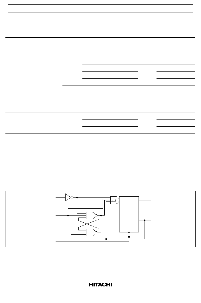
Logic Diagram
A
B
CLR
Q
Q
Q
CLR
Q
HD74LV221A
5
DC Electrical Characteristics
·
Ta = 40 to 85
°
C
Item
Symbol
V
CC
(V)*
Min
Typ
Max
Unit
Test Conditions
Input voltage
V
IH
2.0
1.5
--
--
V
2.3 to 2.7
V
CC
×
0.7
--
--
3.0 to 3.6
V
CC
×
0.7
--
--
4.5 to 5.5
V
CC
×
0.7
--
--
V
IL
2.0
--
--
0.5
2.3 to 2.7
--
--
V
CC
×
0.3
3.0 to 3.6
--
--
V
CC
×
0.3
4.5 to 5.5
--
--
V
CC
×
0.3
Output voltage
V
OH
Min to
Max
V
CC
0.1
--
--
V
I
OL
=
50
µ
A
2.3
2.0
--
--
I
OL
=
2 mA
3.0
2.48
--
--
I
OL
=
6 mA
4.5
3.8
--
--
I
OL
=
12 mA
V
OL
Min to
Max
--
--
0.1
V
I
OL
= 50
µ
A
2.3
--
--
0.4
I
OL
= 2 mA
3.0
--
--
0.44
I
OL
= 6 mA
4.5
--
--
0.55
I
OL
= 12 mA
Input current
I
IN
0 to 5.5
--
--
±
1
µ
A
V
IN
= 5.5 V or GND
Input current
Rext / Cext
I
IN
5.5
--
--
±
2.5
µ
A
V
IN
= V
CC
or GND
Quiescent
supply current
I
CC
5.5
--
--
20
µ
A
V
IN
= V
CC
or GND, I
O
= 0
Active state
supply
current
(per circuit)
I
CC
2.3
--
--
220
µ
A
V
IN
= V
CC
or GND
Rext/Cext = 0.5 V
CC
3.0
280
4.5
650
5.5
975
Output leakage
current
I
OFF
0
--
--
5
µ
A
V
O
= 5.5 V
Input
capacitance
C
IN
3.3
--
4.0
--
pF
V
I
= V
CC
or GND
Note:
For conditions shown as Min or Max, use the appropriate values under recommended operating
conditions.