Preliminary: The specification of this device are subject to change without notice. Please contact your
nearest Hitachi's Sales Dept. regarding specification.
HM628128DI Series
1 M SRAM (128-kword
◊
8-bit)
ADE-203-999A (Z)
Preliminary
Rev. 0.1
Jul. 8, 1999
Description
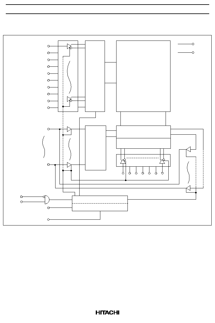
The Hitachi HM628128DI Series is 1-Mbit static RAM organized 131,072-kword
◊
8-bit. HM628128DI
Series has realized higher density, higher performance and low power consumption by employing Hi-CMOS
process technology. The HM628128DI Series offers low power standby power dissipation; therefore, it is
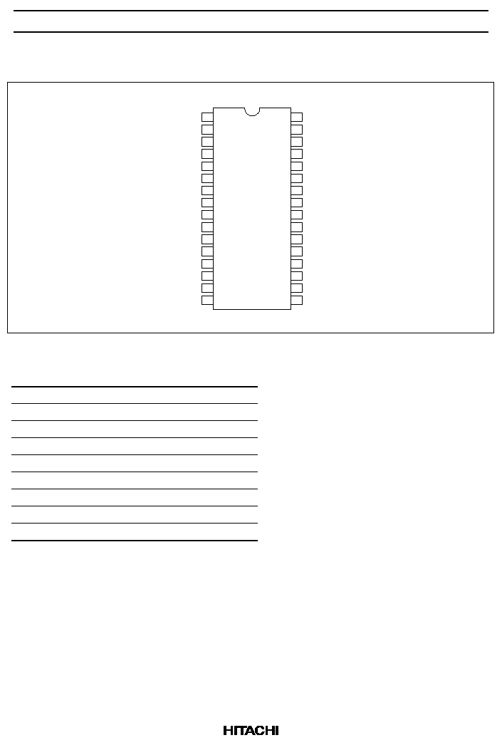
suitable for battery backup systems. It has package variations of standard 32-pin plastic DIP, standard 32-pin
plastic SOP.
Features
∑
Single 5 V supply: 5 V
±
10%
∑
Access time: 70 ns (max)
∑
Power dissipation
Active: 30 mW/MHz (typ)
Standby: 10
µ
W (typ)
∑
Completely static memory.
No clock or timing strobe required
∑
Equal access and cycle times
∑
Common data input and output
Three state output
∑
Directly TTL compatible all inputs
∑
Battery backup operation
2 chip selection for battery backup
∑
Temperature range: ≠40 to +85
∞
C

HM628128DI Series
5
Operation Table
CS1
CS2
WE
OE
I/O
Operation
H
◊
◊
◊
High-Z
Standby
◊
L
◊
◊
High-Z
Standby
L
H
H
L
Dout
Read
L
H
L
H
Din
Write
L
H
L
L
Din
Write
L
H
H
H
High-Z
Output disable
Note:
H: V
IH
, L: V
IL
,
◊
: V
IH
or V
IL
Absolute Maximum Ratings
Parameter
Symbol
Value
Unit
Power supply voltage relative to V
SS
V
CC
≠0.5 to +7.0
V
Terminal voltage on any pin relative to V
SS
V
T
≠0.5*
1
to V
CC
+ 0.3*
2
V
Power dissipation
P
T
1.0
W
Storage temperature range
Tstg
≠55 to +125
∞
C
Storage temperature range under bias
Tbias
≠40 to +85
∞
C
Notes: 1. V
T
min: ≠1.5 V for pulse half-width
30 ns
2. Maximum voltage is +7.0 V
DC Operating Conditions
Parameter
Symbol
Min
Typ
Max
Unit
Note
Supply voltage
V
CC
4.5
5.0
5.5
V
V
SS
0
0
0
V
Input high voltage
V
IH
2.4
--
V
CC
+ 0.3
V
Input low voltage
V
IL
≠0.3
--
0.6
V
1
Ambient temperature range
Ta
≠40
--
85
∞
C
Note:
1. V
IL
min: ≠1.5 V for pulse half-width
30 ns