 | –≠–ª–µ–∫—Ç—Ä–æ–Ω–Ω—ã–π –∫–æ–º–ø–æ–Ω–µ–Ω—Ç: PF0121 | –°–∫–∞—á–∞—Ç—å:  PDF PDF  ZIP ZIP |
PF0121
MOS FET Power Amplifier Module for GSM Mobile Phone
ADE-208-097A (Z)
2nd Edition
July 1996
Application
For GSM CLASS2 890 to 915 MHz
Features
∑
Low power control current: 0.9 mA Typ
∑
High speed switching: 1.5
µ
sec Typ
∑
Wide power control range: 100 dB Typ
Pin Arrangement
1
2
3
4
5
5
1: Pin
2: V
APC
3: V
DD
4: Pout
5: GND
∑
RF-B2
PF0121
2
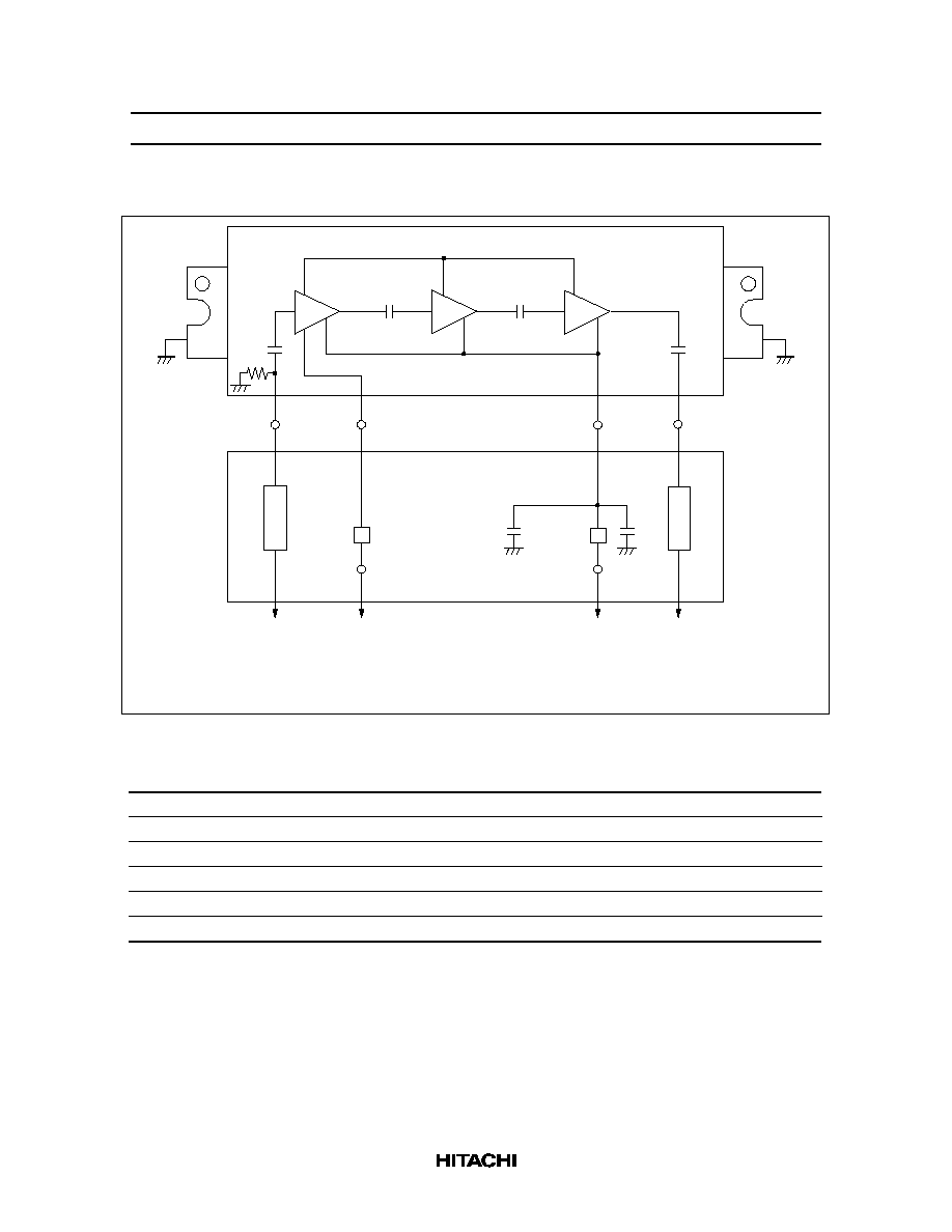
Internal Diagram and External Circuit
G
GND
G
GND
Pin1
Pin
Pin2
V
APC
Pin3
V
DD
Pin4
Pout
Pout
V
DD
V
APC
Pin
Z1
C2
C1
Z2
FB1
FB2
C1 = 0.01
µ
F (Ceramic chip capacitor)
C2 = 330
µ
F (Aluminum Electrolyte Capacitor)
FB = Ferrite bead BL01RN1-A62-001 (Manufacture: MURATA) or equivalent
Z1 = Z2 = 50
(Microstrip line)
Absolute Maximum Ratings (Tc = 25∞C)
Item
Symbol
Rating
Unit
Supply voltage
V
DD
17
V
Supply current
I
DD
6
A
APC voltage
V
APC
8
V
Input power
Pin
20
mW
Operating case temperature
Tc (op)
≠30 to +110
∞
C
Storage temperature
Tstg
≠40 to +110
∞
C
PF0121
3
Electrical Characteristics (Tc = 25∞C)
Item
Symbol
Min
Typ
Max
Unit
Test Condition
Drain cutoff current
I
DS
--
--
500
µ
A
V
DD
= 17 V, V
APC
= 0 V
Total efficiency
T
30
35
--
%
Pin =
2 mW, V
DD
= 12.5 V,
2nd harmonic distortion
2nd H.D.
--
≠50
≠40
dBc
Pout = 13 W (at APC controlled),
3rd harmonic distortion
3rd H.D.
--
≠55
≠45
dBc
R
L
= Rg = 50
, Tc = 25
∞
C
Input VSWR
VSWR (in) --
2
3
--
Output power (1)
Pout (1)
17
23
--
W
Pin =
2 mW, V
DD
= 12.5 V, V
APC
= 7 V,
R
L
=Rg = 50
, Tc = 25
∞
C
Output power (2)
Pout (2)
9
12
--
W
Pin =
2 mW, V
DD
= 10.3V, V
APC
= 7 V,
R
L
= Rg = 50
, Tc = 80
∞
C
Isolation
--
--
≠60
≠40
dBm
Pin =
2 mW, V
DD
= 12.5 V, V
APC
= 0.5 V,
R
L
= Rg = 50
, Tc = 25
∞
C
Switching time
t
r
, t
f
--
1.5
2
µ
s
Pin =
2 mW, V
DD
= 12.5 V, Pout = 13 W,
R
L
= Rg = 50
, Tc = 25
∞
C
Stability
--
No parasitic oscillation --
Pin =
2 mW, V
DD
= 12.5 V,
Pout
13 W (at APC controlled),
Rg = 50
, Tc = 25
∞
C,
Output VSWR = 20:1 All phases
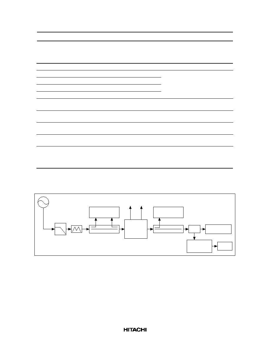
Test System Diagram
S.G
L.P.F
3dB
ATT
Power
Meter
Test
Fixture
RF SW.
Power Meter
Phase
Shifter
Directional
Coupler
V
APC
V
DD
Directional
Coupler
Spectrum
Analyzer
Short
PF0121
4
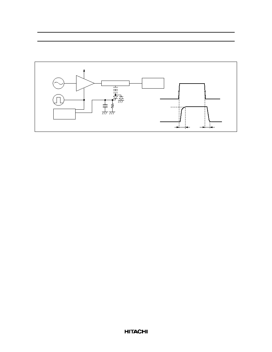
Switching Time Test Diagram
S.G
P.G
Oscillo
Scope
Vout
f=10 kHz
V
APC
Pin
Pout
D.U.T
V
DD
=12.5 V
Z=50
2p
2p
1SS106
1SS106
2.2 k
100p
Power
Meter
Vout
95%
50%
50%
5%
tr
tf
Duty=1/8
V
APC
PF0121
5
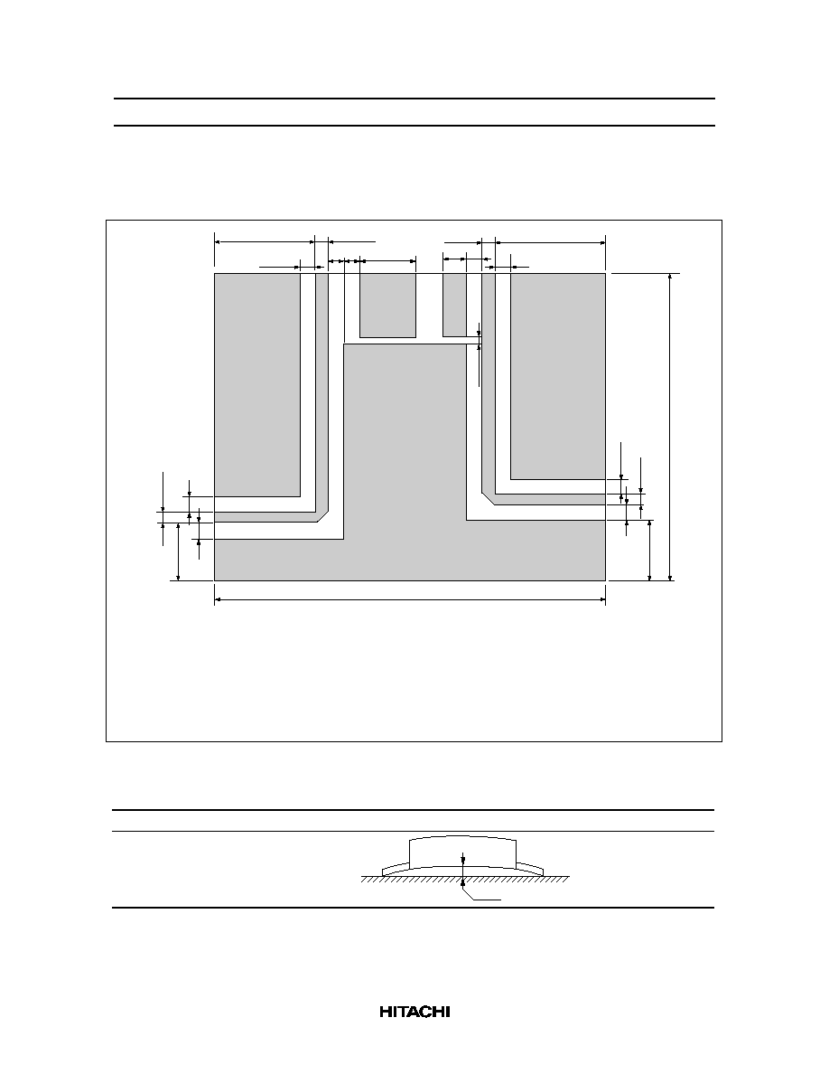
Test Fixture Pattern
Unit: mm
100
3.5
4
16.5
80
2.88
4
4
15
2.88
26.5
3.5
2.88
16
3
4.5
2.88
28
4
6
4
V
APC
V
DD
1.5
Grass Epoxy Double sided PCB
(t = 1.6 mm,
r = 4.8)
C1=0.01
µ
F (Ceramic Chip Capacitor)
C2=330
µ
F (Aluminum Electrolyte Capacitor)
L1=L2 : BLO2RN1-R62 (Manufacturer : MURATA) or equivalent (Ferrite Bead Inductor)
The coefficient of RF line loss in the P.C.B is showed bellow.
1/ (S
21
)
2
= 1/ (0.9805)
2
= 1.068
Mechanical Characteristics
Item
Conditions
Spec
Torque for screw up the heatsink flange
M3 Screw Bolts
4 to 6 kg∑cm
Warp size of the heatsink flange: S
S
S = 0
+0.3/≠0 mm