 | –≠–ª–µ–∫—Ç—Ä–æ–Ω–Ω—ã–π –∫–æ–º–ø–æ–Ω–µ–Ω—Ç: TBB1004 | –°–∫–∞—á–∞—Ç—å:  PDF PDF  ZIP ZIP |

TBB1004
Twin Build in Biasing Circuit MOS FET IC
VHF/UHF RF Amplifier
ADE-208-988H (Z)
9th. Edition
Dec. 2000
Features
∑
Small SMD package CMPAK-6 built in twin BBFET; To reduce using parts cost & PC board space.
∑
Suitable for World Standard Tuner RF amplifier.
∑
Very useful for total tuner cost reduction.
∑
Withstanding to ESD; Build in ESD absorbing diode. Withstand up to 200V at C=200pF, Rs=0
conditions.
∑
Provide mini mold packages; CMPAK-6
Outline
CMPAK-6
3
1
6
4
1. Drain(1)
2. Source
3. Gate-1(1)
4. Gate-1(2)
5. Gate-2
6. Drain(2)
2
5
Notes:
1.
Marking is "DM".
2.
TBB1004 is individual type number of HITACHI TWIN BBFET.

TBB1004
2
Absolute Maximum Ratings (Ta = 25∞C)
Item
Symbol
Ratings
Unit
Drain to source voltage
V
DS
6
V
Gate1 to source voltage
V
G1S
+6
-0
V
Gate2 to source voltage
V
G2S
+6
-0
V
Drain current
I
D
30
mA
Channel power dissipation
Pch
*3
250
mW
Channel temperature
Tch
150
∞
C
Storage temperature
Tstg
≠55 to +150
∞
C
Notes: 3. Value on the glass epoxy board (49mm
◊
38mm
◊
1mm).
Electrical Characteristics (Ta = 25∞C)
The below specification are applicable for UHF unit (FET1)
Item
Symbol
Min
Typ
Max
Unit
Test Conditions
Drain to source breakdown
voltage
V
(BR)DSS
6
--
--
V
I
D
= 200
µ
A, V
G1S
= V
G2S
= 0
Gate1 to source breakdown
voltage
V
(BR)G1SS
+6
--
--
V
I
G1
= +10
µ
A, V
G2S
= V
DS
= 0
Gate2 to source breakdown
voltage
V
(BR)G2SS
+6
--
--
V
I
G2
= +10
µ
A, V
G1S
= V
DS
= 0
Gate1 to source cutoff current
I
G1SS
--
--
+100
nA
V
G1S
= +5V, V
G2S
= V
DS
= 0
Gate2 to source cutoff current
I
G2SS
--
--
+100
nA
V
G2S
= +5V, V
G1S
= V
DS
= 0
Gate1 to source cutoff voltage V
G1S(off)
0.5
0.7
1.0
V
V
DS
= 5V, V
G2S
= 4V, I
D
= 100
µ
A
Gate2 to source cutoff voltage V
G2S(off)
0.5
0.7
1.0
V
V
DS
= 5V, V
G1S
= 5V, I
D
= 100
µ
A
Drain current
I
D(op)
13
17
21
mA
V
DS
= 5V, V
G1
= 5V
V
G2S
= 4V, R
G
= 100k
Forward transfer admittance
|y
fs
|
21
26
31
mS
V
DS
= 5V, V
G1
= 5V, V
G2S
=4V
R
G
= 100k
, f = 1kHz
Input capacitance
c
iss
1.4
1.8
2.2
pF
V
DS
= 5V, V
G1
= 5V
Output capacitance
c
oss
1.0
1.4
1.8
pF
V
G2S
=4V, R
G
= 100k
Reverse transfer capacitance
c
rss
--
0.02
0.04
pF
f = 1MHz
Power gain
PG
16
21
--
dB
V
DS
= V
G1
= 5V, V
G2S
= 4V
R
G
= 100k
, f = 900MHz
Zi=S11*, Zo=S22*(:PG)
Noise figure
NF
--
1.7
2.5
dB
Zi=S11opt (:NF)

TBB1004
3
Electrical Characteristics (Ta = 25∞C)
The below specification are applicable for VHF unit (FET2)
Item
Symbol
Min
Typ
Max
Unit
Test Conditions
Drain to source breakdown
voltage
V
(BR)DSS
6
--
--
V
I
D
= 200
µ
A, V
G1S
= V
G2S
= 0
Gate1 to source breakdown
voltage
V
(BR)G1SS
+6
--
--
V
I
G1
= +10
µ
A, V
G2S
= V
DS
= 0
Gate2 to source breakdown
voltage
V
(BR)G2SS
+6
--
--
V
I
G2
= +10
µ
A, V
G1S
= V
DS
= 0
Gate1 to source cutoff current
I
G1SS
--
--
+100
nA
V
G1S
= +5V, V
G2S
= V
DS
= 0
Gate2 to source cutoff current
I
G2SS
--
--
+100
nA
V
G2S
= +5V, V
G1S
= V
DS
= 0
Gate1 to source cutoff voltage V
G1S(off)
0.5
0.75
1.0
V
V
DS
= 5V, V
G2S
= 4V, I
D
= 100
µ
A
Gate2 to source cutoff voltage V
G2S(off)
0.5
0.75
1.0
V
V
DS
= 5V, V
G1S
= 5V, I
D
= 100
µ
A
Drain current
I
D(op)
16
20
24
mA
V
DS
= 5V, V
G1
= 5V, V
G2S
= 4V,
R
G
= 100k
Forward transfer admittance
|y
fs
|
27
32
37
mS
V
DS
= 5V, V
G1
= 5V, V
G2S
=4V
R
G
= 100k
, f = 1kHz
Input capacitance
c
iss
2.3
2.7
3.1
pF
V
DS
= 5V, V
G1
= 5V
Output capacitance
c
oss
1.4
1.8
2.2
pF
V
G2S
=4V, R
G
= 100k
Reverse transfer capacitance
c
rss
--
0.03
0.05
pF
f = 1MHz
Power gain
PG
24
29
--
dB
V
DS
= V
G1
= 5V, V
G2S
= 4V
Noise figure
NF
--
1.2
1.7
dB
R
G
= 100k
, f = 200MHz
TBB1004
4
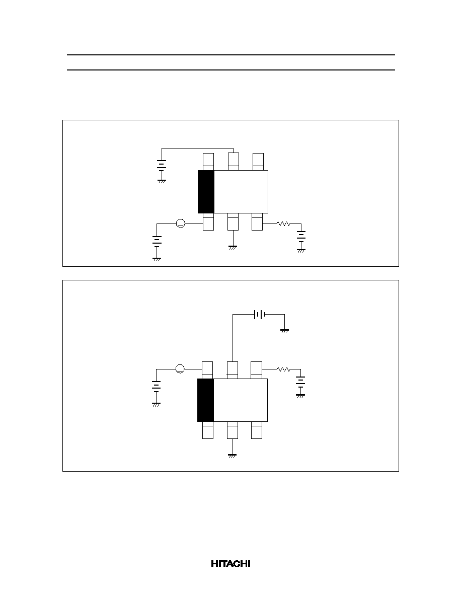
Test Circuits
∑
DC Biasing Circuit for Operating Characteristic Items (I
D(op)
, |yfs|, Ciss, Coss, Crss, NF, PG)
Measurment of FET1
Gate 1
Source
Gate 2
R
G
Drain
A
I
D
V
G2
V
G1
V
D
Open
Open
Measurment of FET2
Gate 1
Source
Gate 2
Drain
V
G2
R
G
V
G1
A
I
D
V
D
Open
Open
TBB1004
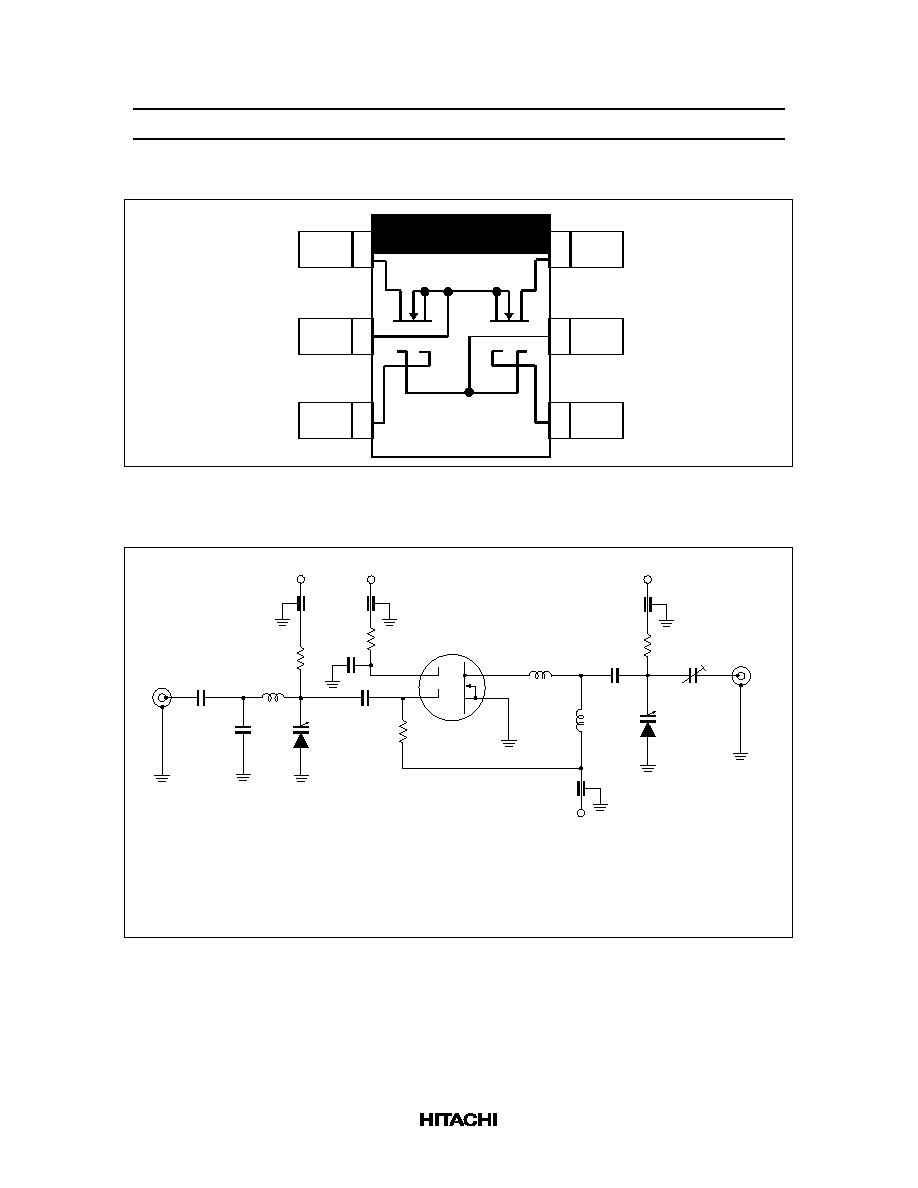
5
∑
Equivalent Circuit
BBFET-(1)
BBFET-(2)
No.1
No.2
No.3
No.6
No.5
No.4
Gate-1(1)
Source
Drain(1)
Gate-1(2)
Gate-2
Drain(2)
∑
200 MHz Power Gain, Noise Figure Test Circuit
V
G2
Input (50
)
1000p
36p
1000p
L1
V = V
D G1
R
G
TWINBBFET
RFC
Output (50
)
L2
1000p
10p max
1000p
1000p
47k
1SV70
1000p
1000p
1000p
47k
47k
100k
V
T
V
T
Unit : Resistance (
)
Capacitance (F)
1SV70
L1 :
1mm Enameled Copper Wire,Inside dia 10mm, 2Turns
L2 :
1mm Enameled Copper Wire,Inside dia 10mm, 2Turns
RFC :
1mm Enameled Copper Wire,Inside dia 5mm, 2Turns

TBB1004
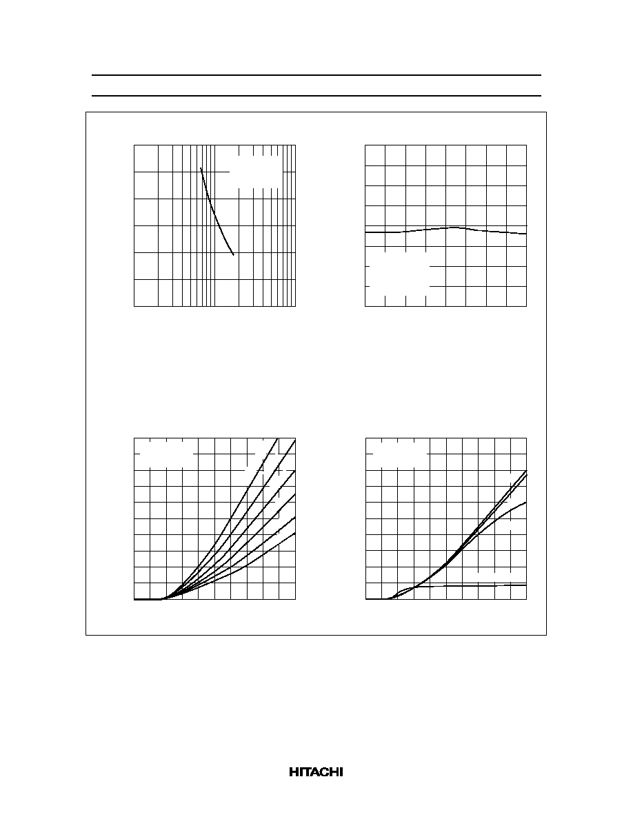
6
400
300
200
100
0
50
100
150
200
0
1
2
3
4
5
25
20
15
10
5
V = 4 V
V = V
G2S
G1
DS
25
20
15
10
5
0
1
2
3
4
5
50
40
30
20
10
0
1
2
3
4
5
V = 5 V
R = 100 k
DS
G
V = 5 V
DS
Channel Power Dissipation Pch* (mW)
Ambient Temperature Ta (
∞
C)
Maximum Channel Power
Dissipation Curve
Drain Current I (mA)
D
Typical Output Characteristics (FET1)
Drain to Source Voltage V (V)
DS
Drain Current vs.
Gate1 Voltage (FET1)
Gate1 Voltage V (V)
G1
Drain Current I (mA)
D
R = 68 k
G
82 k
100 k
2 V
V = 1 V
G2S
4 V
3 V
* Value on the glass epoxy board (49mm
◊
38mm
◊
1mm)
120 k
150 k
180 k
Gate1 Voltage V (V)
G1
Forward Transfer Admittance
vs. Gate1 Voltage (FET1)
fs
Forward Transfer Admittance |y | (mS)
V = 4 V
G2S
150 k
R = 68 k
G
100 k
TBB1004
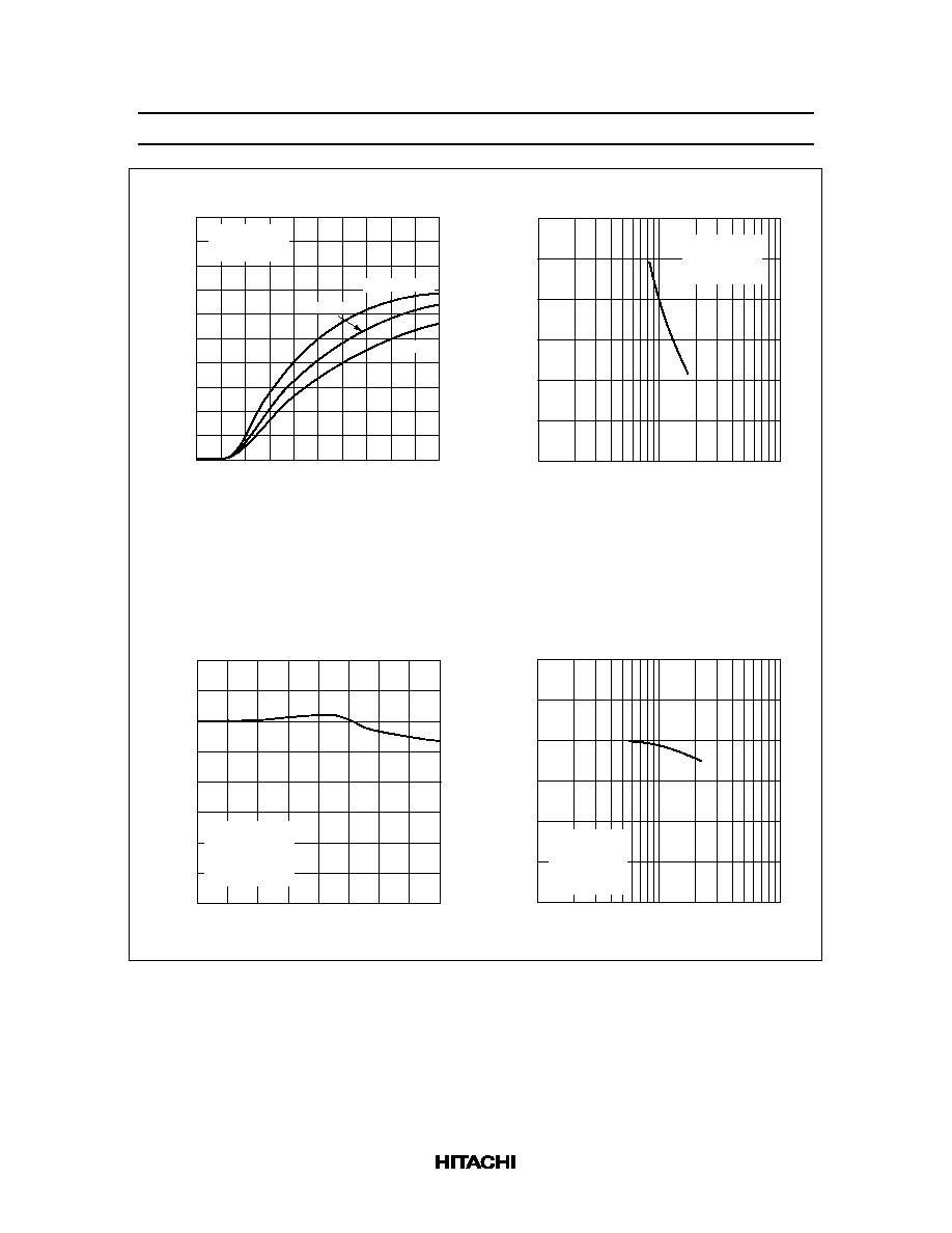
7
0
1
2
3
4
4
3
2
1
0
Gate2 to Source Voltage V (V)
G2S
Input Capacitance Ciss (pF)
Input Capacitance vs.
Gate2 to Source Voltage (FET1)
0
1
2
3
4
5
25
20
15
10
5
V = 4 V
V = V
G2S
G1
DS
Drain Current I (mA)
D
Typical Output Characteristics (FET2)
Drain to Source Voltage V (V)
DS
R = 68 k
G
100 k
120 k
150 k
82 k
25
20
15
10
5
0
1
2
3
4
5
V = 5 V
R = 100 k
DS
G
Drain Current vs.
Gate1 Voltage (FET2)
Gate1 Voltage V (V)
G1
Drain Current I (mA)
D
2 V
V = 1 V
G2S
4 V
3 V
30
25
20
15
10
5
0
10
20
50
100 200
500 1000
V = 5 V
V = 5 V
V = 4 V
DS
G1
G2S
Drain Current vs.
Gate Resistance (FET1)
Drain Current I (mA)
D
Gate Resistance R (k
)
G
180 k
V = 5 V
V = 5 V
R = 100 k
f = 1 MHz
DS
G1
G
TBB1004
8
50
40
30
20
10
0
1
2
3
4
5
V = 5 V
DS
Gate1 Voltage V (V)
G1
Forward Transfer Admittance
vs. Gate1 Voltage (FET2)
fs
Forward Transfer Admittance |y | (mS)
V = 4 V
G2S
150 k
R = 68 k
G
0
1
2
3
4
4
3
2
1
0
Gate2 to Source Voltage V (V)
G2S
Input Capacitance Ciss (pF)
Input Capacitance vs.
Gate2 to Source Voltage (FET2)
30
25
20
15
10
5
0
10
20
50
100 200
500 1000
V = 5 V
V = 5 V
V = 4 V
DS
G1
G2S
Drain Current vs.
Gate Resistance (FET2)
Drain Current I (mA)
D
Gate Resistance R (k
)
G
40
35
30
25
20
15
10
10
20
50
100 200
500 1000
V = 5 V
V = 5 V
V = 4 V
f = 200 MHz
DS
G1
G2S
Power Gain vs.
Gate Resistance (FET2)
Gate Resistance R (k
)
G
Power Gain PG (dB)
100 k
V = 5 V
V = 5 V
R = 100 k
f = 1 MHz
DS
G1
G
TBB1004
9
0
4
3
2
1
10
20
50
100 200
500 1000
V = 5 V
V = 5 V
V = 4 V
f = 200 MHz
DS
G1
G2S
Noise Figure vs.
Gate Resistance (FET2)
Noise Figure NF (dB)
Gate Resistance R (k
)
G
4
0
10
20
30
40
50
3
2
1
0
DS
G
V = V = 5 V
R = 100 k
G1
Gain Reduction GR (dB)
Gain Reduction vs.
Gate2 to Source Voltage (FET2)
Gate2 to Source Voltage V (V)
G2S

TBB1004
10
Package Dimensions
2.1
±
0.3
6-0.2
0.9
±
0.1
(0.2)
2.0
±
0.2
(0.65)
(0.65)
1.3
±
0.2
(0.425)
(0.425)
Hitachi Code
JEDEC
EIAJ
Mass (reference value)
CMPAK-6
--
Conforms
0.006 g
0.15
0 to 0.1
+ 0.1
≠ 0.05
+ 0.1
≠ 0.05
1.25
±
0.1
As of January, 2001
Unit: mm
TBB1004
11
Cautions
1. Hitachi neither warrants nor grants licenses of any rights of Hitachi's or any third party's patent,
copyright, trademark, or other intellectual property rights for information contained in this document.
Hitachi bears no responsibility for problems that may arise with third party's rights, including
intellectual property rights, in connection with use of the information contained in this document.
2. Products and product specifications may be subject to change without notice. Confirm that you have
received the latest product standards or specifications before final design, purchase or use.
3. Hitachi makes every attempt to ensure that its products are of high quality and reliability. However,
contact Hitachi's sales office before using the product in an application that demands especially high
quality and reliability or where its failure or malfunction may directly threaten human life or cause risk
of bodily injury, such as aerospace, aeronautics, nuclear power, combustion control, transportation,
traffic, safety equipment or medical equipment for life support.
4. Design your application so that the product is used within the ranges guaranteed by Hitachi particularly
for maximum rating, operating supply voltage range, heat radiation characteristics, installation
conditions and other characteristics. Hitachi bears no responsibility for failure or damage when used
beyond the guaranteed ranges. Even within the guaranteed ranges, consider normally foreseeable
failure rates or failure modes in semiconductor devices and employ systemic measures such as fail-
safes, so that the equipment incorporating Hitachi product does not cause bodily injury, fire or other
consequential damage due to operation of the Hitachi product.
5. This product is not designed to be radiation resistant.
6. No one is permitted to reproduce or duplicate, in any form, the whole or part of this document without
written approval from Hitachi.
7. Contact Hitachi's sales office for any questions regarding this document or Hitachi semiconductor
products.
Hitachi, Ltd.
Semiconductor & Integrated Circuits.
Nippon Bldg., 2-6-2, Ohte-machi, Chiyoda-ku, Tokyo 100-0004, Japan
Tel: Tokyo (03) 3270-2111 Fax: (03) 3270-5109
Copyright
©
Hitachi, Ltd., 2000. All rights reserved. Printed in Japan.
Hitachi Asia Ltd.
Hitachi Tower
16 Collyer Quay #20-00,
Singapore 049318
Tel : <65>-538-6533/538-8577
Fax : <65>-538-6933/538-3877
URL : http://www.hitachi.com.sg
URL
NorthAmerica
: http://semiconductor.hitachi.com/
Europe
: http://www.hitachi-eu.com/hel/ecg
Asia
: http://sicapac.hitachi-asia.com
Japan
: http://www.hitachi.co.jp/Sicd/indx.htm
Hitachi Asia Ltd.
(Taipei Branch Office)
4/F, No. 167, Tun Hwa North Road,
Hung-Kuo Building,
Taipei (105), Taiwan
Tel : <886>-(2)-2718-3666
Fax : <886>-(2)-2718-8180
Telex : 23222 HAS-TP
URL : http://www.hitachi.com.tw
Hitachi Asia (Hong Kong) Ltd.
Group III (Electronic Components)
7/F., North Tower,
World Finance Centre,
Harbour City, Canton Road
Tsim Sha Tsui, Kowloon,
Hong Kong
Tel : <852>-(2)-735-9218
Fax : <852>-(2)-730-0281
URL : http://www.hitachi.com.hk
Hitachi Europe Ltd.
Electronic Components Group.
Whitebrook Park
Lower Cookham Road
Maidenhead
Berkshire SL6 8YA, United Kingdom
Tel: <44> (1628) 585000
Fax: <44> (1628) 585160
Hitachi Europe GmbH
Electronic Components Group
Dornacher Stra
e 3
D-85622 Feldkirchen, Munich
Germany
Tel: <49> (89) 9 9180-0
Fax: <49> (89) 9 29 30 00
Hitachi Semiconductor
(America) Inc.
179 East Tasman Drive,
San Jose,CA 95134
Tel: <1> (408) 433-1990
Fax: <1>(408) 433-0223
For further information write to:
Colophon 2.0