 | –≠–Ľ–Ķ–ļ—ā—Ä–ĺ–Ĺ–Ĺ—č–Ļ –ļ–ĺ–ľ–Ņ–ĺ–Ĺ–Ķ–Ĺ—ā: HT24LC04 | –°–ļ–į—á–į—ā—Ć:  PDF PDF  ZIP ZIP |
Document Outline
- Ģˇ
- Ģˇ
- Ģˇ
- Ģˇ
- Ģˇ
- Ģˇ
- Ģˇ
- Ģˇ
- Ģˇ
- Ģˇ
- Ģˇ
- Ģˇ
HT24LC04
CMOS 4K 2-Wire Serial EEPROM
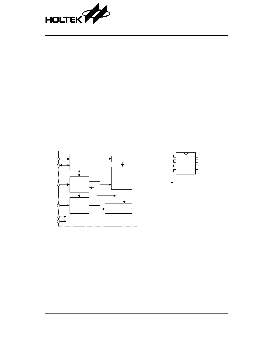
Block Diagram
Pin Assignment
Rev. 1.30
1
November 25, 2003
Features
∑
Operating voltage: 2.2V~5.5V
∑
Low power consumption
-
Operation: 5mA max.
-
Standby: 5
mA max.
∑
Internal organization: 512
ī8
∑
2-wire serial interface
∑
Write cycle time: 5ms max.
∑
Automatic erase-before-write operation
∑
Partial page write allowed
∑
16-byte page write modes
∑
Write operation with built-in timer
∑
Hardware controlled write protection
∑
40-year data retention
∑
10
6
erase/write cycles per word
∑
Commercial temperature range (0
įC to +70įC)
∑
8-pin DIP/SOP package
General Description
The HT24LC04 is a 4K-bit serial read/write non-volatile
memory device using the CMOS floating gate process.
Its 4096 bits of memory are organized into 512 words
and each word is 8 bits. The device is optimized for use
in many industrial and commercial applications where
low power and low voltage operation are essential. Up
to four HT24LC04 devices may be connected to the
same two-wire bus. The HT24LC04 is guaranteed for
1M erase/write cycles and 40-year data retention.
1
2
3
4
8
7
6
5
A 0
A 1
A 2
V S S
V C C
W P
S C L
S D A
H T 2 4 L C 0 4
8 D I P - A / S O P - A
I / O
C o n t r o l
L o g i c
M e m o r y
C o n t r o l
L o g i c
S C L
S D A
A d d r e s s
C o u n t e r
A 0 ~ A 2
V C C
V S S
X
D
E
C
E E P R O M
A r r a y
P a g e B u f
Y D E C
S e n s e A M P
R / W C o n t r o l
H V P u m p
W P
Pin Description
Pin No.
Pin Name
I/O
Description
1~3
A0~A2
I
Address inputs
4
VSS
ĺ
Negative power supply
5
SDA
I/O
Serial data inputs/output
6
SCL
I
Serial clock data input
7
WP
I
Write protect
8
VCC
ĺ
Positive power supply
Absolute Maximum Ratings
Operating Temperature (Commercial) ........................................................................................................ 0
įC to 70įC
Storage Temperature ............................................................................................................................
-50įC to 125įC
Applied V
CC
Voltage with Respect to VSS ..................................................................................V
SS
-0.3V to V
CC
+6.0V
Applied Voltage on any Pin with Respect to VSS
.................................................................................................
V
SS
-0.3V to V
CC
+0.3V
Note: These are stress ratings only. Stresses exceeding the range specified under
≤Absolute Maximum Ratings≤ may
cause substantial damage to the device. Functional operation of this device at other conditions beyond those
listed in the specification is not implied and prolonged exposure to extreme conditions may affect device reliabil-
ity.
D.C. Characteristics
Ta=0
įC to 70įC
Symbol
Parameter
Test Conditions
Min.
Typ.
Max.
Unit
V
CC
Conditions
V
CC
Operating Voltage
ĺ
ĺ
2.2
ĺ
5.5
V
I
CC1
Operating Current
5V
Read at 100kHz
ĺ
ĺ
2
mA
I
CC2
Operating Current
5V
Write at 100kHz
ĺ
ĺ
5
mA
V
IL
Input Low Voltage
ĺ
ĺ
-1
ĺ
0.3V
CC
V
V
IH
Input High Voltage
ĺ
ĺ
0.7V
CC
ĺ
V
CC
+0.5
V
V
OL
Output Low Voltage
2.4V
I
OL
=2.1mA
ĺ
ĺ
0.4
V
I
LI
Input Leakage Current
5V
V
IN
=0 or V
CC
ĺ
ĺ
1
mA
I
LO
Output Leakage Current
5V
V
OUT
=0 or V
CC
ĺ
ĺ
1
mA
I
STB1
Standby Current
5V
V
IN
=0 or V
CC
ĺ
ĺ
5
mA
I
STB2
Standby Current
2.4V
V
IN
=0 or V
CC
ĺ
ĺ
4
mA
C
IN
Input Capacitance (See Note)
ĺ
f=1MHz 25
į
C
ĺ
ĺ
6
pF
C
OUT
Output Capacitance (See Note)
ĺ
f=1MHz 25
į
C
ĺ
ĺ
8
pF
Note: These parameters are periodically sampled but not 100% tested
HT24LC04
Rev. 1.30
2
November 25, 2003

A.C. Characteristics
Ta=0
įC to 70įC
Symbol
Parameter
Standard Mode*
V
CC
=5V
Ī10%
Unit
Remark
Min.
Max.
Min.
Max.
f
SK
Clock Frequency
ĺ
100
ĺ
400
kHz
ĺ
t
HIGH
Clock High Time
4000
ĺ
600
ĺ
ns
ĺ
t
LOW
Clock Low Time
4700
ĺ
1200
ĺ
ns
ĺ
t
r
SDA and SCL Rise Time
ĺ
1000
ĺ
300
ns
Note
t
f
SDA and SCL Fall Time
ĺ
300
ĺ
300
ns
Note
t
HD:STA
START Condition Hold Time
4000
ĺ
600
ĺ
ns
After this period the first
clock pulse is generated
t
SU:STA
START Condition Setup Time
4000
ĺ
600
ĺ
ns
Only relevant for repeated
START condition
t
HD:DAT
Data Input Hold Time
0
ĺ
0
ĺ
ns
ĺ
t
SU:DAT
Data Input Setup Time
200
ĺ
100
ĺ
ns
ĺ
t
SU:STO
STOP Condition Setup Time
4000
ĺ
600
ĺ
ns
ĺ
t
AA
Output Valid from Clock
ĺ
3500
ĺ
900
ns
ĺ
t
BUF
Bus Free Time
4700
ĺ
1200
ĺ
ns
Time in which the bus
must be free before a new
transmission can start
t
SP
Input Filter Time Constant
(SDA and SCL Pins)
ĺ
100
ĺ
50
ns
Noise suppression time
t
WR
Write Cycle Time
ĺ
5
ĺ
5
ms
ĺ
Note:
These parameters are periodically sampled but not 100% tested
* The standard mode means V
CC
=2.2V to 5.5V
For relative timing, refer to timing diagrams
HT24LC04
Rev. 1.30
3
November 25, 2003
Functional Description
∑
Serial clock (SCL)
The SCL input is used for positive edge clock data into
each EEPROM device and negative edge clock data
out of each device.
∑
Serial data (SDA)
The SDA pin is bidirectional for serial data transfer.
The pin is open-drain driven and may be wired-OR
with any number of other open-drain or open collector
devices.
∑
A0, A1, A2
The HT24LC04 uses the A2 and A1 inputs for hard
wire addressing and a total of four 4K devices may be
addressed on a single bus system. The A0 pin is not
connected. (The device addressing is discussed in
detail under the Device Addressing section).
∑
Write protect (WP)
The HT24LC04 has a write protect pin that provides
hardware data protection. The write protect pin allows
normal read/write operations when connected to the
V
SS
. When the write protect pin is connected to Vcc,
the write protection feature is enabled and operates
as shown in the following table.
WP Pin Status
Protect Array
At V
CC
Full Array (4K)
At V
SS
Normal Read/Write Operations
Memory Organization
∑
HT24LC04, 4K Serial EEPROM
Internally organized with 512 8-bit words, random
word addressing requires a 9-bit data word address.
Device Operations
∑
Clock and data transition
Data transfer may be initiated only when the bus is not
busy. During data transfer, the data line must remain
stable whenever the clock line is high. Changes in
data line while the clock line is high will be interpreted
as a START or STOP condition.
HT24LC04
Rev. 1.30
4
November 25, 2003
∑
Start condition
A high-to-low transition of SDA with SCL high is a start
condition which must precede any other command
(refer to Start and Stop Definition Timing diagram).
∑
Stop condition
A low-to-high transition of SDA with SCL high is a stop
condition. After a read sequence, the stop command
will place the EEPROM in a standby power mode (re-
fer to Start and Stop Definition Timing Diagram).
∑
Acknowledge
All addresses and data words are serially transmitted
to and from the EEPROM in 8-bit words. The
EEPROM sends a zero to acknowledge that it has re-
ceived each word. This happens during the ninth
clock cycle.
Device Addressing
The 4K EEPROM devices require an 8-bit device ad-
dress word following a start condition to enable the chip
for a read or write operation. The device address word
consist of a mandatory one, zero sequence for the first
four most significant bits (refer to diagram showing the
Device Address). This is common to all the EEPROM
device.
The next three bits are the A2, A1 and A0 device ad-
dress bits for the 1K/2K EEPROM. These three bits
must compare to their corresponding hard-wired input
pins.
The 4K EEPROM only use the A2 and A1 device ad-
dress bits with the third bit as a memory page address
bit. The two device address bits must compare to their
corresponding hardwired input pins. The A0 pin is not
connected.
The 8th bit of device address is the read/write operation
select bit. A read operation is initiated if this bit is high
and a write operation is initiated if this bit is low.
If the comparison of the device address succeed the
EEPROM will output a zero at ACK bit. If not, the chip
will return to a standby state.
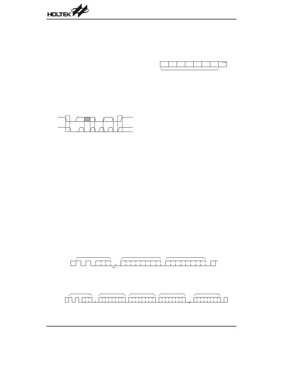
Write Operations
∑
Byte write
A write operation requires an 8-bit data word address
following the device address word and acknowledg-
ment. Upon receipt of this address, the EEPROM will
again respond with a zero and then clock in the first
8-bit data word. After receiving the 8-bit data word, the
EEPROM will output a zero and the addressing de-
vice, such as a microcontroller, must terminate the
write sequence with a stop condition. At this time the
EEPROM enters an internally-timed write cycle to the
non-volatile memory. All inputs are disabled during
this write cycle and EEPROM will not respond until the
write is completed (refer to Byte write timing).
∑
Page write
The 4K device is capable of 16-byte page writes. A page
write is initiated the same as byte write, but the
microcontroller does not send a stop condition after
the first data word is clocked in. Instead, after the
EEPROM acknowledges the receipt of the first data
word, the microcontroller can transmit up to fifteen
more data words. The EEPROM will respond with a
z e r o a f t e r e a c h d a t a w o r d r e c e i v e d . T h e
microcontroller must terminate the page write se-
quence with a stop condition.
The data word address lower four bits are internally in-
cremented following the receipt of each data word.
The higher data word address bits are not incre-
mented, retaining the memory page row location (re-
fer to Page write timing).
S C L
S D A
D a t a a l l o w e d
t o c h a n g e
A d d r e s s o r
a c k n o w l e d g e
v a l i d
S t o p
c o n d i t i o n
S t a r t
c o n d i t i o n
N o A C K
s t a t e
R / W
1
0
A 2
A 1
A 0
D e v i c e A d d r e s s
1
0
R / W
A 2 A 1 A 0
S
P
D e v i c e a d d r e s s
W o r d a d d r e s s
D A T A
A C K
S t o p
S t a r t
S D A
A C K
A C K
Byte Write Timing
P
D e v i c e a d d r e s s
W o r d a d d r e s s
D A T A n
A C K
S t o p
S t a r t
S D A
A C K
A C K
S
A C K
D A T A n + 1
D A T A n + x
Page Write Timing

HT24LC04
Rev. 1.30
5
November 25, 2003
∑
Acknowledge polling
To maximize bus throughput, one technique is to allow
the master to poll for an acknowledge signal after the
start condition and the control byte for a write com-
mand have been sent. If the device is still busy imple-
menting its write cycle, then no ACK will be returned.
The master can send the next read/write command
when the ACK signal has finally been received.
∑
Write protect
The HT24LC04 has a write-protect function and pro-
gramming will then be inhibited when the WP pin is
connected to VCC. Under this mode, the HT24LC04 is
used as a serial ROM.
∑
Read operations
The HT24LC04 supports three read operations,
namely, current address read, random address read
and sequential read. During read operation execution,
the read/write select bit should be set to
≤1≤.
∑
Current address read
The internal data word address counter maintains the
last address accessed during the last read or write op-
eration, incremented by one. This address stays valid
between operations as long as the chip power is main-
tained. The address roll over during read from the last
byte of the last memory page to the first byte of the first
page. The address roll over during write from the last
byte of the current page to the first byte of the same
page. Once the device address with the read/write se-
lect bit set to one is clocked in and acknowledged by
the EEPROM, the current address data word is seri-
ally clocked out. The microcontroller should respond
with a
≤no ACK≤ signal (high) followed by a stop condi-
tion (refer to Current read timing).
∑
Random read
A random read requires a dummy byte write sequence
to load in the data word address which is then clocked
in and acknowledged by the EEPROM. The
microcontroller must then generate another start con-
dition. The microcontroller now initiates a current ad-
dress read by sending a device address with the
read/write select bit high. The EEPROM acknowl-
edges the device address and serially clocks out the
data word. The microcontroller should respond with a
≤no ACK≤ signal (high) followed by a stop condition
(refer to Random read timing).
A 2 A 1 A 0
S
P
D e v i c e a d d r e s s
D A T A
A C K
S t o p
S t a r t
S D A
N o A C K
Current Read Timing
P
D e v i c e a d d r e s s
W o r d a d d r e s s
A C K
S t o p
S t a r t
S D A
A C K
N o A C K
S
A C K
D A T A
S
A 2 A 1 A 0
D e v i c e a d d r e s s
S t a r t
Random Read Timing
S e n d W r i t e C o m m a n d
S e n d S t o p C o n d i t i o n
t o I n i t i a t e W r i t e C y c l e
S e n d S t a r t
S e n d C o t r o l l B y t e
w i t h R / W = 0
( A C K = 0 ) ?
N e x t O p e r a t i o n
N o
Y e s
Acknowledge Polling Flow