 | ÐлекÑÑоннÑй компоненÑ: HT815D0 | СкаÑаÑÑ:  PDF PDF  ZIP ZIP |
Äîêóìåíòàöèÿ è îïèñàíèÿ www.docs.chipfind.ru

HT815D0
11.2-Second LOG-PCM Speech
1
March 15, 2000
Features
·
Operating voltage: 2.4V~5.0V
·
Directly drives an external transistor
·
Low standby current (1mA typ. for V
DD
=3V)
·
Minimal external components
·
508 words table ROM for key functions
·
Programmable silence length and end-pulse
width (minimal end-pulse width is 330ms at a
6kHz sampling rate)
·
11.2-second voice capacity (based on a 6kHz
sampling rate)
·
FLAG1 options
End-pulse output
3HzB flash
6HzB flash
Voice output indication
Busy output
·
FLAG2 options
3Hz flash
6Hz flash
Busy output
·
Controllable volume
·
12 keys
·
Key options
Stop key: KEY12
Random (only for KEY1)
Sequential (only for KEY1)
Repeat (for all KEYs)
Key debounce time (for all KEYs): 700ms,
22ms, 45ms, 180ms (based on a sampling
rate of 6kHz)
One shot (for all KEYs)
Level-trigger
Pull-high resistance (for all KEYs)
·
Section options
Retriggerable
Non-retriggerable
·
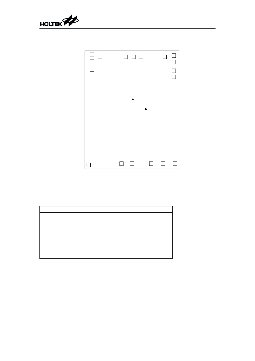
Dice form or 16/20/24-pin DIP,
20/24-pin SOP package
General Description
The HT815D0 is a single chip LOG-PCM voice
synthesizer LSI with 11.2-second voice capacity
at 6kHz sampling rate. The chip when trig-
gered drives a speaker through an external
transistor with a current switch D/A converter
output. Negligible current will be consumed in
the standby state.
The HT815D0 provides 12 key inputs and 2 pro-
grammable FLAG outputs. With a 2.4V~5.0V
power supply, a complete synthesized voice
playback system can be easily built with very
few external components.
The customer¢s voice sources are recorded sec-
tion by section into an internal mask ROM. The
sectional playback arrangement instructions of
each key are stored in the table ROM. The key
features are also programmable. With such a
flexible structure, the HT815D0 is excellent for
versatile voice applications.
Applications
·
Leisure products
·
Alarm clocks
·
Public address system
·
Alert & warning system
·
Sound effect generators
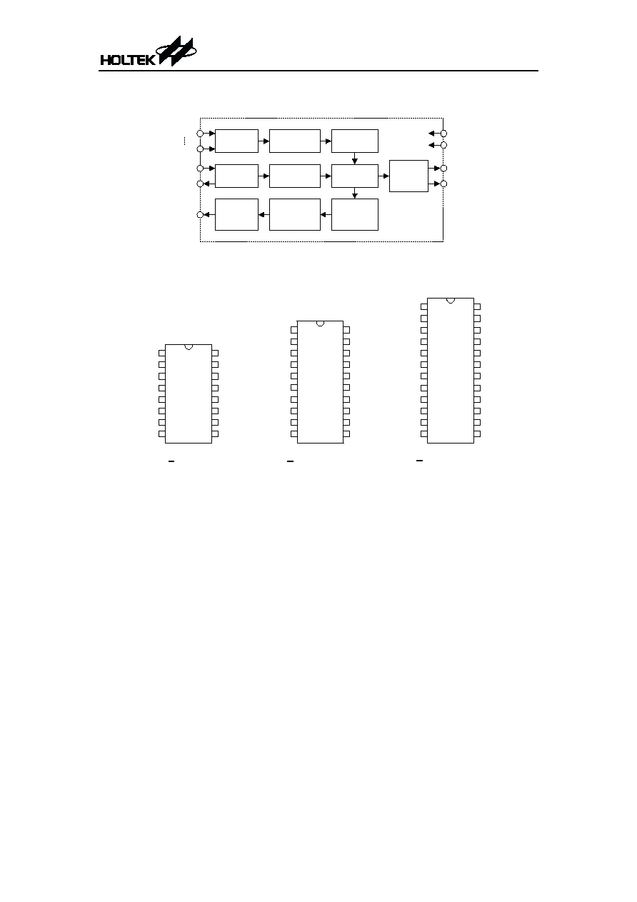
Block Diagram
Pin Assignment
HT815D0
2
March 15, 2000
1 6
1 5
1 4
1 3
1 2
1 1
1 0
9
1
2
3
4
5
6
7
8
N C
N C
N C
N C
V D D
A U D
O S C 2
O S C 1
N C
N C
K E Y 3
K E Y 2
K E Y 1
F L A G 2
V S S
F L A G 1
K E Y 6
K E Y 5
K E Y 4
K E Y 3
K E Y 2
K E Y 1
F L A G 2
V S S
F L A G 1
O S C 1
2 0
1 9
1 8
1 7
1 6
1 5
1 4
1 3
1 2
1 1
1
2
3
4
5
6
7
8
9
1 0
K E Y 7
K E Y 8
K E Y 9
K E Y 1 0
K E Y 1 1
K E Y 1 2
N C
V D D
A U D
O S C 2
K E Y 6
K E Y 5
K E Y 4
K E Y 3
K E Y 2
K E Y 1
N C
N C
N C
N C
F L A G 2
V S S
2 4
2 3
2 2
2 1
2 0
1 9
1 8
1 7
1 6
1 5
1 4
1 3
1
2
3
4
5
6
7
8
9
1 0
1 1
1 2
K E Y 7
K E Y 8
K E Y 9
K E Y 1 0
K E Y 1 1
K E Y 1 2
N C
V D D
A U D
O S C 2
O S C 1
F L A G 1
H T 8 1 5 D 0
1 6 D I P
H T 8 1 5 D 0
2 0 D I P / S O P
H T 8 1 5 D 0
2 4 D I P / S O P
D e b o u n c e
C i r c u i t
O n e - s h o t
K e y T a b l e
O s c i l l a t o r
C i r c u i t
T i m e B a s e
G e n e r a t o r
T a b l e R O M
5 0 8 ´ 1 3 - b i t
D A C &
O u t p u t
C o n t r o l
S p e e c h R O M
6 4 K ´ 6 - b i t
R O M
A d d r e s s
C o u n t e r
K E Y 1
K E Y 1 2
A U D
S t a t u s
D i s p l a y
C o n t r o l l e r
F L A G 1
F L A G 2
V D D
V S S
O S C 1
O S C 2
Pad Assignment
Chip size: 2270 ´ 2840 (mm)
2
* The IC substrate should be connected to VSS in the PCB layout artwork.
Pad Coordinates
Unit: mm
Pad No.
X
Y
Pad No.
X
Y
1
-914.50
1216.45
11
912.80
719.65
2
-914.50
1073.05
12
912.80
858.25
3
-914.50
882.45
13
912.80
1053.65
4
-987.90
-1241.95
14
912.80
1197.25
5
-254.60
-1215.45
15
709.50
1167.75
6
-18.90
-1215.45
16
179.20
1167.75
7
411.90
-1215.45
17
22.00
1167.75
8
674.70
-1215.45
18
-156.40
1167.75
9
806.10
-1246.05
19
-734.20
1167.75
10
937.90
-1215.45
HT815D0
3
March 15, 2000
1
2
3
4
5
6
7
8
9 1 0
1 1
1 2
1 3
1 4
1 5
1 6
1 7
1 8
1 9
( 0 , 0 )
K E Y 1 0
K E Y 1 1
K E Y 1 2
V D D
KE
Y9
KE
Y7
KE
Y8
KE
Y6
KE
Y5
K E Y 4
K E Y 3
K E Y 2
K E Y 1
FL
A
G
2
VS
S
FL
A
G
1
OS
C
1
OS
C
2
AU
D
Pad Description
Pad No.
Pad Name
I/O
Internal
Connection
Description
1~3
KEY10~KEY12 I
Pull-high
Trigger key, active low. Key features such as
debounce time, pull-high resistance and repeat are
all by mask option.
4
VDD
¾
¾
Positive power supply
5
AUD
O
PMOS
Open Drain Voice output for driving an external transistor
6
OSC2
O
¾
Oscillator output pin
7
OSC1
I
¾
Oscillator input pin
8
FLAG1
O
NMOS
Open Drain
3HzB/6HzB flash output, busy output, end-pulse
or voice output indication (by mask option). Open
drain, active low output
9
VSS
¾
¾
Negative power supply, ground
10
FLAG2
O
NMOS
Open Drain
3Hz/6Hz flash output or busy output (by mask op-
tion). Open drain, active low output
11~19
KEY1~KEY9
I
Pull-high
Trigger key, active low. Key features such as
debounce time, pull-high resistance and repeat are
all by mask option.
Absolute Maximum Ratings
Supply Voltage ............................... -0.3V to 6V
Storage Temperature ............... -50°C to 125°C
Input Voltage ............... V
SS
-0.3V to V
DD
+0.3V
Operating Temperature ............ -20°C to 70°C
Note: These are stress ratings only. Stresses exceeding the range specified under ²Absolute Maxi-
mum Ratings² may cause substantial damage to the device. Functional operation of this device
at other conditions beyond those listed in the specification is not implied and prolonged expo-
sure to extreme conditions may affect device reliability.
HT815D0
4
March 15, 2000
Electrical Characteristics
Ta=25°C
Symbol
Parameter
Test Conditions
Min.
Typ.
Max.
Unit
V
DD
Conditions
V
DD
Operating Voltage
¾
¾
2.4
¾
5.0
V
I
DD
Operating Current
3V
No load
¾
200
400
mA
I
STB
Standby Current
3V
¾
¾
1
3
mA
I
O
Max. AUD Output Current
3V
V
OH
=0.6V
-1.5
-2
¾
mA
I
OL
FLAG Sink Current
3V
V
OL
=0.3V
1.5
3.0
¾
mA
V
IH
²H² Input Voltage
¾
¾
0.8V
DD
¾
V
DD
V
V
IL
²L² Input Voltage
¾
¾
0
¾
0.2V
DD
V
f
OSC
Oscillating Frequency
3V
R
OSC
=530kW
76
96
116
kHz
HT815D0
5
March 15, 2000
Functional Description
The HT815D0 is a mask ROM type voice synthe-
sizer with 11.2-second voice capacity. A group of
pre-recorded voice sections is played upon receipt
of key trigger input signals. Two FLAG signals
are output while playing voices.
The 11.2-second voice capacity can be divided
into sections of arbitrary length. Notice that the
silence length and end-pulse width are not in-
cluded in the memory.
By using Holtek¢s programming tools, the con-
tents and arrangement of sections, key features
and FLAG output are all programmable before
device fabrication.
The IC provides 12 key inputs (KEY1~KEY12).
Of the 12 keys, KEY1 can be optioned as a di-
rect, sequential or random trigger key. KEY12
can be selected as a stop or direct key. The re-
maining 10 keys (KEY2~KEY11), are used as
direct keys exclusively.
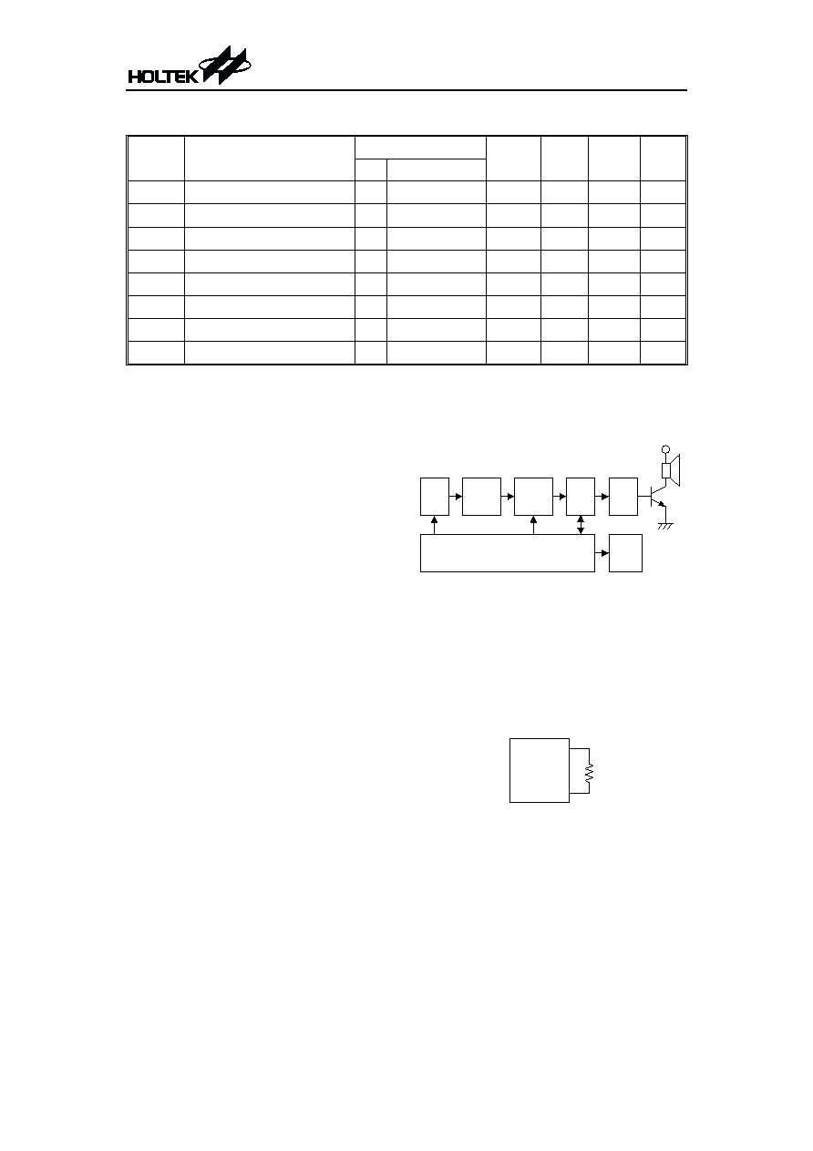
Play function block diagram
System oscillator
The HT815D0 has a built-in RC oscillator which
requires only one external resistor for normal ap-
plications. The oscillator frequency is typically
96kHz for an external resistor of 530kW. The re-
quired oscillator frequency may vary with differ-
ent sampling rates in the process of voice
programming. As a result, the value of the oscilla-
tor resistor may be different for different items.
K e y
t r i g g e r
K e y
f e a t u r e s
o p t i o n
K e y
f u n c t i o n
t a b l e
R O M
V o i c e
R O M
D / A
P l a y c o n t r o l l o g i c
F l a g
o u t p u t
V
D D
H T 8 1 5 D 0
O S C 1
O S C 2
R
O S C
Document Outline
- þÿ
- þÿ
- þÿ
- þÿ
- þÿ
- þÿ
- þÿ
- þÿ
- þÿ
- þÿ
- þÿ
- þÿ