 | ÐлекÑÑоннÑй компоненÑ: HT82P604B | СкаÑаÑÑ:  PDF PDF  ZIP ZIP |
Äîêóìåíòàöèÿ è îïèñàíèÿ www.docs.chipfind.ru

HT82P604B
DC-DC Converter
1
March 23, 2000
Preliminary
Pentium is a trademark of Intel Corporation
Features
·
Operating voltage: 5V~12V
·
Drives two N-Channel MOSFETs
·
Simple single-loop control design
-
Voltage-mode PWM control
·
Fast transient response
-
High-bandwidth error amplifier
-
Full 0% to 100% duty ratio
·
Excellent output voltage regulation
-
±1% over line voltage and temperature
·
5 bit digital-to-analog output voltage selection
-
Wide range -1.3V to 3.5V
-
0.1V binary steps from 2.1V to 3.5V
-
0.05V binary steps from 1.3V to 2.05V
·
Power-good output voltage monitor
·
Over-voltage and over-current sensing ele-
ment, uses MOSFET¢s r
DS (ON)
·
Small converter size
-
Constant frequency operation
-
200kHz free-running oscillator program-
mable from 50kHz to over 1MHz
Applications
·
Power supply for Pentium
TM
, Pentium
TM
Pro, PowerPC
TM
and Alpha
TM
Microproces-
sors
·
High-power5Vto3.xVDC-DCregulators
·
Low-voltage distributed power supplies
General Description
The HT82P604B provides complete control and
protection for a DC-DC converter optimized for
high performance microprocessor applications.
It is designed to drive two N-Channel
MOSFETs in a synchronous-rectified buck to-
pology. The HT82P604B integrates all of the
control, output adjustment, monitoring and
protection functions into a single package.
The output voltage of the converter is easily ad-
justed and precisely regulated. The HT82P604B
includes a 5-input digital-to-analog converter
(DAC) that adjusts the output voltage from 2.1V
to 3.5V in 0.1V increments and from 1.3V to
2.05V in 0.05V steps. The precision reference
and voltage-mode regulator hold the selected
output voltage to within ±1% over temperature
andlinevoltagevariations.
The HT82P604B provides simple, single feed-
back loop, voltage-mode control with fast tran-
sient response. It includes a 200kHz
free-running triangle-wave oscillator that is
adjustable from below 50kHz to over 1MHz.
The error amplifier features a 15MHz
gain-bandwidth product and 6V/ms slew rate
which enables high converter bandwidth for
fast transient performance. The resulting
PWM duty ratio ranges from 0% to 100%.
The HT82P604B monitors the output voltage
with a window comparator that tracks the DAC
output and issues a Power Good signal when
the output is within ±10%. The HT82P604B
protects against over-current conditions by in-
hibiting PWM operation. Built-in over-voltage
protection triggers an external SCR to crowbar
the input supply. The HT82P604B monitors the
current by using the r
DS (ON)
of the upper
MOSFET which eliminates the need for a cur-
rent sensing resistor.
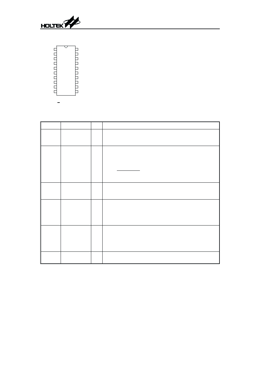
Pin Assignment
Pin Description
Pin No.
Pin Name
I/O
Description
1
VSEN
I
This pin is connected to the converters output voltage. The
PGOOD and OVP comparator circuits use this signal to report
output voltage status and for overvoltage protection.
2
OCSET
I
Connect a resistor (R
OCSET
) from this pin to the drain of the up-
per MOSFET. R
OCSET
, an internal 200mA current source
(I
OCS
), and the upper MOSFET on-resistance (r
DS (ON)
) set the
converter over-current (OC) trip point.
I
= I
R
r
PEAK
OCS
OCSET
DS(ON)
´
An over-current trip cycles the soft-start function.
3
SS
O
Connect a capacitor from this pin to ground. This capacitor,
along with an internal 10mA current source, sets the soft-start
interval of the converter.
4~8
VID0~4
I
VID0-4 are the input pins to the 5-bit DAC. The states of these
five pins program the internal voltage reference (DACOUT).
The level of DACOUT sets the converter output voltage. It also
sets the PGOOD and OVP thresholds. Table 1 specifies
DACOUT for the 32 combinations of DAC inputs.
9, 10
COMP, FB
I
COMP and FB are the available external pins of the error ampli-
fier. The FB pin is the inverting input of the error amplifier and
the COMP pin is the error amplifier output. These pins are used
to compensate the voltage-control feedback loop of the con-
verter.
11
GND
P
Signal ground for the IC. All voltage levels are measured with
respect to this pin.
HT82P604B
2
March 23, 2000
Preliminary
V S E N
O C S E T
S S
V I D 0
V I D 1
V I D 2
V I D 3
V I D 4
C O M P
F B
R T
O V P
V C C
L G A T E
P G N D
B O O T
U G A T E
P H A S E
P G O O D
G N D
2 0
1 9
1 8
1 7
1 6
1 5
1 4
1 3
1 2
1 1
1
2
3
4
5
6
7
8
9
1 0
H T 8 2 P 6 0 4 B
2 0 S O P
Pin No.
Pin Name
I/O
Description
12
PGOOD
O
PGOOD is an open collector output used to indicate the status of
the converter output voltage. This pin is pulled low when the
converter output is not within ±10% of the DACOUT reference
voltage. Exception to this behavivor is the ¢11111¢ VID pin com-
bination which disables the converter; in this case, PGOOD as-
serts a high level.
13
PHASE
O
Connect the PHASE pin to the upper MOSFET source. This pin
is used to monitor the voltage drop across the MOSFET for
over-current protection. This pin also provides the return path
for the upper gate drive.
14
UGATE
O
Connect UGATE to the upper MOSFET gate. This pin provides
the gate drive for the upper MOSFET.
15
BOOT
I
This pin provides bias voltage to the upper MOSFET driver. A
bootstrap circuit may be used to create a BOOT voltage suitable
to drive a standard N-Channel MOSFET.
16
PGND
P
This is the power ground connection. Tie the lower MOSFET
source to this pin.
17
LGATE
O
Connect LGATE to the lower MOSFET gate. This pin provides
the gate drive for the lower MOSFET.
18
VCC
P
Provide a 12V bias supply for the chip to this pin.
19
OVP
O
The OVP pin can be used to drive an external SCR in the event
of an overvoltage condition.
20
RT
I
This pin provides oscillator switching frequency adjustment. By
placing a resistor (R
T
) from this pin to GND, the nominal
200kHz switching frequency is increased.
F
S
» 200kHz + 5 10
R (k )
6
T
´
W
(R
T
to GND)
Conversely, connecting a pull-up resistor (R
T
) from this pin to
VCC reduces the switching frequency.
F
S
» 200kHz + 4 10
R (k )
7
T
´
W
(R
T
to 12V)
Absolute Maximum Ratings
Supply Voltage ......................................... +15V
Storage Temperature ............... -50°C to 125°C
Input Voltage ............... GND-0.3 to V
CC
+0.3V
Operating Temperature ............ -20°C to 75°C
Note: These are stress ratings only. Stresses exceeding the range specified under ²Absolute Maxi-
mum Ratings² may cause substantial damage to the device. Functional operation of this device
at other conditions beyond those listed in the specification is not implied and prolonged expo-
sure to extreme conditions may affect device reliability.
HT82P604B
3
March 23, 2000
Preliminary
Electrical Characteristics
Symbol
Parameter
Test Conditions
Min. Typ. Max. Unit
V
CC
Conditions
V
CC
Supply Current
I
CC
Nominal Supply
12V Ugate and Lgate Open
¾
5
¾
mA
Power-On Reset
Rising V
CC
Threshold
12V V
OCSET
=4.5V
¾
¾
10.4
V
Falling V
CC
Threshold
12V V
OCSET
=4.5V
8.2
¾
¾
V
Rising V
OCSET
Threshold
12V
¾
1.26
¾
V
Oscillator
Free Running Frequency
12V RT=Open
185
200
215
kHz
Total Variation
12V 6kW<RT to GND<200kW -15
¾
+15
%
DV
OSC
Ramp Amplitude
12V RT=Open
¾
1.9
¾
V
P-P
Reference and DAC
DACOUT Voltage Accuracy 12V
-1.0
¾
+1.0
%
ERROR Amplifier
DC Gain
12V
¾
88
¾
dB
GBW
Gain-Bandwidth Product
12V
¾
15
¾
MHz
SR
Slew Rate
12V COMP=10pF
¾
6
¾
V/ms
Gate Drivers
I
UGATE
Upper Gate Source
12V V
BOOT
-V
PHASE
=12V,
V
UGATE
=6V
350
500
¾
mA
R
UGATE
Upper Gate Sink
12V I
LGATE
=0.3A
¾
5.5
10
W
I
LGATE
Lower Gate Source
12V V
CC
=12V, V
LGATE
=6V
300
450
¾
mA
R
LGATE
Lower Gate Sink
12V I
LGATE
=0.3V
¾
3.5
6.5
W
Protection
Over-Voltage Trip
(V
SEN
/DACOUT)
12V
¾
115
120
%
I
OCSET
OCSET Current Source
12V V
OCSET
=4.5V
DC
170
200
230
mA
I
OVP
OVP Sourcing Current
12V V
SEN
=5.5, V
OVP
=0V
60
¾
¾
mA
I
SS
Soft Start Current
12V
¾
10
¾
mA
Power Good
Upper Threshold
(V
SEN
/DACOUT)
12V V
SEN
Rising
106
¾
111
%
HT82P604B
4
March 22, 2000
Preliminary
Symbol
Parameter
Test Conditions
Min. Typ. Max. Unit
V
CC
Conditions
Lower Threshold
(V
SEN
/DACOUT)
12V V
SEN
Falling
89
¾
94
%
Hysteresis
(V
SEN
/DACOUT)
12V Upper and Lower
Threshold
¾
2
¾
%
V
PGOOD
PGOOD Voltage Low
12V I
PGOOD
=-5mA
¾
0.5
¾
V
HT82P604B
5
March 23, 2000
Preliminary
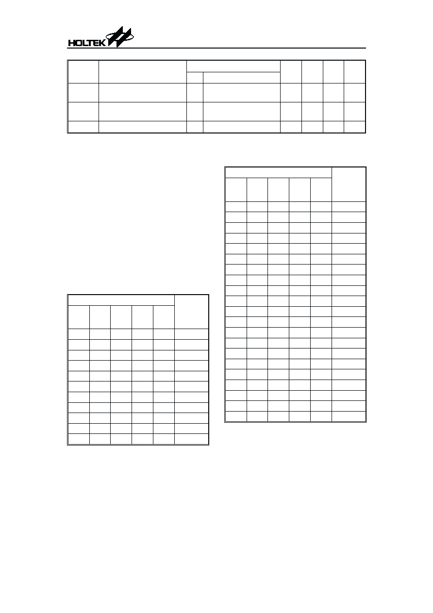
Functional Description
Output voltage program
The output voltage of a HT82P604B converter
is programmed to discrete levels between 1.3V
and 3.5V. The voltage identification (VID) pins
program an internal voltage reference
(DACOUT) with a 5-bit digital-to-analog con-
verter (DAC). The level of DACOUT also sets
the PGOOD and OVP thresholds. Table 1 speci-
fies the DACOUT voltage for the 32 combina-
tions of open or short connections on the VID
pins. The output voltage should not be adjusted
while the converter is delivering power. Re-
move input power before changing the output
voltage. Adjusting the output voltage during
operation could toggle the PGOOD signal and
exercise the overvoltage protection.
Pin Name
Nominal
Output
Voltage
Dacout
VID4 VID3 VID2 VID1 VID0
0
1
1
1
1
1.30
0
1
1
1
0
1.35
0
1
1
0
1
1.40
0
1
1
0
0
1.45
0
1
0
1
1
1.50
0
1
0
1
0
1.55
0
1
0
0
1
1.60
0
1
0
0
0
1.65
0
0
1
1
1
1.70
0
0
1
1
0
1.75
0
0
1
0
1
1.80
Pin Name
Nominal
Output
Voltage
Dacout
VID4 VID3 VID2 VID1 VID0
0
0
1
0
0
1.85
0
0
0
1
1
1.90
0
0
0
1
0
1.95
0
0
0
0
1
2.00
0
0
0
0
0
2.05
1
1
1
1
1
0
1
1
1
1
0
2.1
1
1
1
0
1
2.2
1
1
1
0
0
2.3
1
1
0
1
1
2.4
1
1
0
1
0
2.5
1
1
0
0
1
2.6
1
1
0
0
0
2.7
1
0
1
1
1
2.8
1
0
1
1
0
2.9
1
0
1
0
1
3.0
1
0
1
0
0
3.1
1
0
0
1
1
3.2
1
0
0
1
0
3.3
1
0
0
0
1
3.4
1
0
0
0
0
3.5
Note: 0=connected to GND or VSS, 1=OPEN
Table 1 Output voltage program
Document Outline
- þÿ
- þÿ
- þÿ
- þÿ
- þÿ
- þÿ
- þÿ
- þÿ
- þÿ