HT82V737
16-Bit Stereo Audio D/A Converter with Earphone Driver
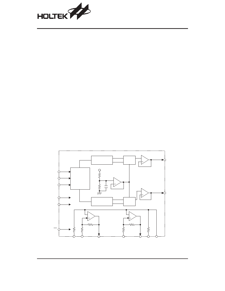
Block Diagram
Rev. 1.00
1
November 26, 2003
Features
·
Wide supply voltage range: 2.4V~5.5V
·
Low power consumption
·
16-bit dynamic range
·
Low total harmonic distortion
·
Stereo audio outputs
·
Data in 2
¢s complement format, TTL
·
Minimum number of external components is required
·
Low clock jitter sensitivity
·
Built-in highly efficient earphone driver
·
16-pin NSOP package
Applications
·
MP3 player
·
CD/VCD ROM and player
·
Satellite/cable STB
·
Digital portable audio/video equipment
General Description
HT82V737 is a low power consumption stereo DAC with
an integrated earphone driver. The device utilizes
CMOS technology specially for portable MP3 players,
VCD and CD machines.
It converts the 16 bits serial data into an analog output
voltage by high precision D/A converter. It can be used
with the Japanese input format: time multiplexed, two
¢s
complement, MSB first TTL level serial input. With its ex-
cellent frequency response characteristics, the
HT82V737 provides users a low cost means of imple-
menting high quality audio voltage outputs. It also builds
in a class AB stereo driver and some application circuits,
thus, requires minimal external components.
The HT82V737 can support low voltage operation at
2.4V so it is very suitable for portable battery powered
audio device. A low supply in power down mode current
reduces power consumption. It is available in small
16-pin NSOP package.
D a t a L a t c h
D A C
O u t
o p
B C K
W S
D I N
D V D D
R C H
L C H
S e r i a l - t o - p a r a l l e l
C o n v e r s i o n
+
V
D D
o p
+
D A C
o p
+
O u t
O u t
D V S S
S e r i a l - t o - p a r a l l e l
C o n v e r s i o n
o p
+
P D
o p
+
2 0 k W
3 0 k W
2 0 k W
3 0 k W
A
V
S
S
R
I
N
R
O
U
T
L
I
N
L
O
U
T
A
V
D
D
B
I
A
S
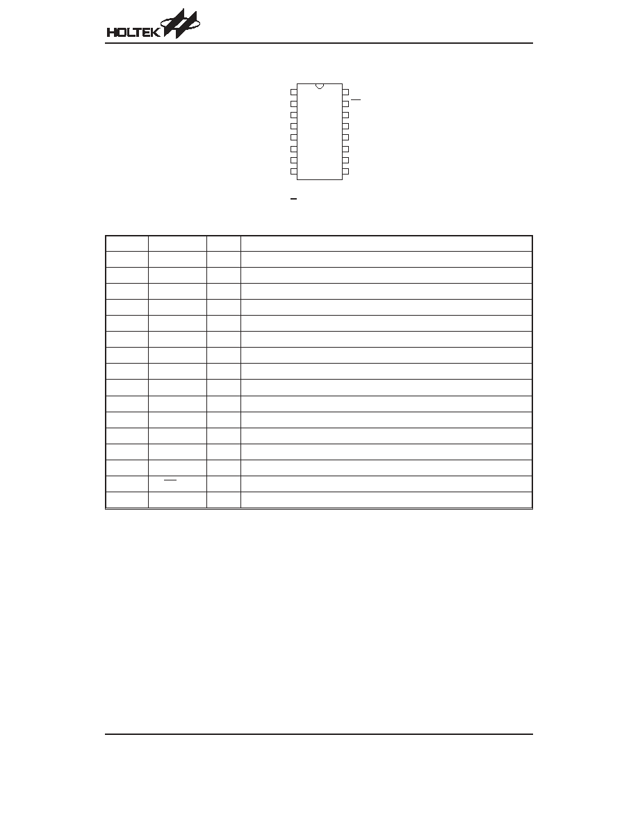
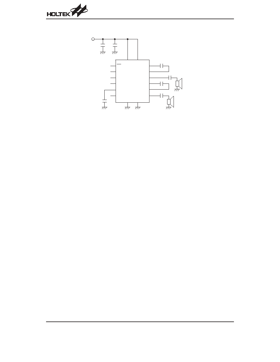
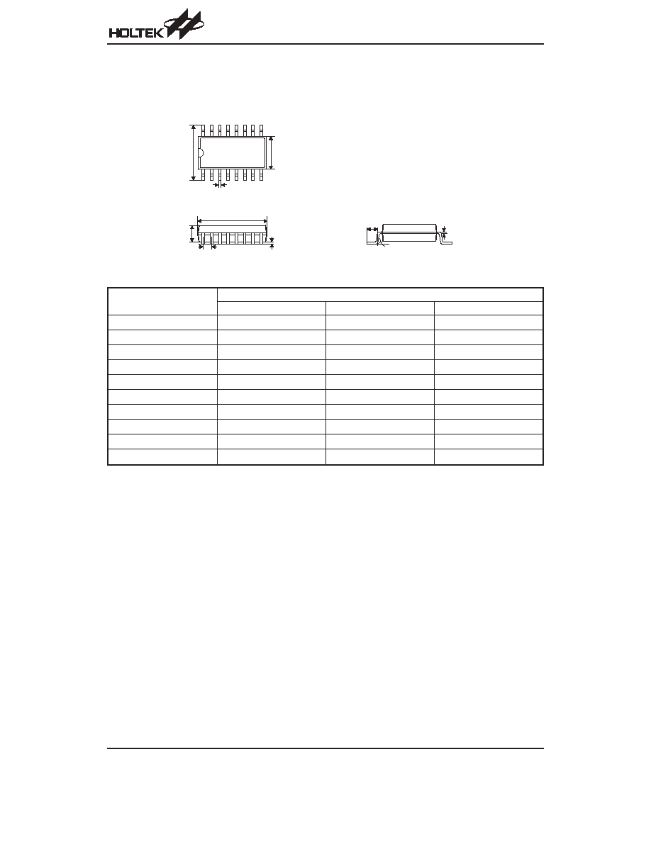
Pin Assignment
Pin Description
Pin No.
Pin Name
I/O
Description
1
WS
I
Word select input
2
DIN
I
Data input
3
DVDD
¾
Digital positive power supply
4
BIAS
¾
Connect a capacitor to ground to increase half-supply stability
5
LCH
O
Left DAC analog output
6
LIN
I
Left inverting output
7
LOUT
O
Left earphone driver analog output
8
AVSS
¾
Analog negative power supply, ground
9
AVDD
¾
Analog positive power supply
10
ROUT
O
Right earphone driver analog output
11
RIN
I
Right inverting input
12
RCH
O
Right DAC analog output
13
NC
¾
No connection
14
DVSS
¾
Digital negative power supply, ground
15
PD
I
When low, the HT82V737 is powered down
16
BCK
I
Bit serial clock input
Absolute Maximum Ratings
Supply Voltage ..........................V
SS
-0.3V to V
SS
+5.5V
Storage Temperature ...........................
-50°C to 125°C
Input Voltage .............................V
SS
-0.3V to V
DD
+0.3V
Operating Temperature ..........................
-20°C to 70°C
Note: These are stress ratings only. Stresses exceeding the range specified under
²Absolute Maximum Ratings² may
cause substantial damage to the device. Functional operation of this device at other conditions beyond those
listed in the specification is not implied and prolonged exposure to extreme conditions may affect device reliabil-
ity.
HT82V737
Rev. 1.00
2
November 26, 2003
W S
D I N
D V D D
B I A S
L C H
L I N
L O U T
A V S S
B C K
P D
D V S S
N C
R C H
R I N
R O U T
A V D D
H T 8 2 V 7 3 7
1 6 N S O P - A
1 6
1 5
1 4
1 3
1 2
1 1
1 0
9
1
2
3
4
5
6
7
8