 | ÐлекÑÑоннÑй компоненÑ: HT9580 | СкаÑаÑÑ:  PDF PDF  ZIP ZIP |
Äîêóìåíòàöèÿ è îïèñàíèÿ www.docs.chipfind.ru

HT9580
Character Pager Controller
1
April 28, 2000
Preliminary
Features
·
Operating voltage: 2.4V~3.5V
·
Temperature range: -30°C to +85°C
·
low power, high performance M6502 core
·
low power crystal oscillator control
-
512/1200/2400 bps data rate operation
·
²CCIR Radio Paging Code No.1² (POCSAG)
compatible
·
76.8kHz crystal for all available data rates
·
High/low system clock switching capability
·
44 Kbytes program ROM
·
848 bytes global data RAM
·
Internal 2 Mbits Character ROM
·
256 Kbits internal SRAM
·
External option up to 2 Mbits Character
ROM or 2 Mbits SRAM
·
SED15X(KSX), MC141X and HD66410
series LCD driver compatible interface
option
·
46 bytes message buffer
·
One 16-bit timer and one 8-bit timer
·
Internal 2Hz or 1Hz RTC or Real Time
Clock option
·
Single buzzer generator output (BZ) with
duty cycle control
·
low current HALT mode operation
·
16-bit watchdog timer
·
Built-in data filter (16-times over-sampling )
and bit clock recovery
·
Advanced synchronization algorithm
·
2-bit random and (optional) 4-bit burst er-
ror correction for address and message
·
Up to 6 user addresses and 6 user frames,
independently programmable
·
3 RF power-on timing control pins
and Received data inversion (optional)
·
Built in SPI circuit
·
Out-of-range condition indicator
·
One internal 8-bit D/A converter
·
Battery fail and battery low detection
·
80-pin LQFP package
General Description
The HT9580 is a high performance pager con-
troller which can be used for Chinese Pager
system applications. The HT9580 4-in-1 Char-
acter Pager Controller combines a POCSAG de-
coder with a M6502 microprocessor core, 2
Mbits Character ROM and 256 Kbits SRAM to
provide both high decoder performance and ex-
cellent system flexibility. The decoder utilizes a
2-bit random error correction algorithm and
therefore provides excellent decoder sensitiv-
ity. The controller contains a full function
pager decoder at a 512, 1200, 2400 bps data
rates. Using an M6502 core takes advantage of
a flexible external control interface, LCD driver
chips and abundant programming resources
from worldwide providers. The internal SPI
would communicate with SPI of FLEX
TM
high
speed pager decoder.
FLEX
TM
is a trademark of Motorola Inc.
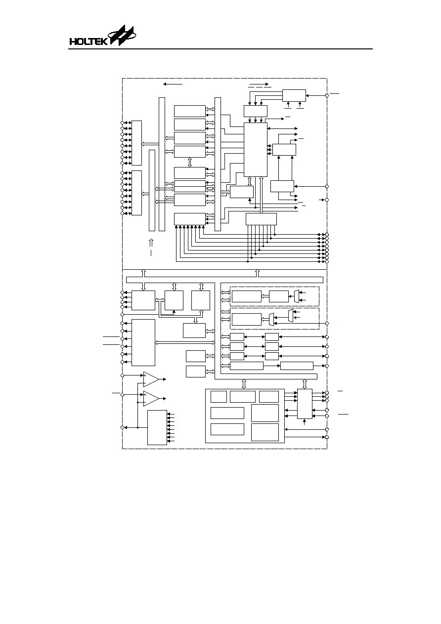
Block Diagram
HT9580
2
April 28, 2000
Preliminary
S y s t e m C l o c k
I R Q N M I
R E S E T
M L
V P
I
n
te
r
n
a
l
A
D
L
P B 0 ~ P B 7
P C 0 ~ P C 1
P A C
P B C
T M R 0 ( 8 b i t )
P C C
MU
X
T M R 1 ( 1 6 b i t )
T M R 1
A 0
A B L
A 1
A 2
A 3
A 4
A 5
A 6
A 7
A 8
A B H
A 9
A 1 0
A 1 1
A 1 2
A 1 3
A 1 4
A 1 5
I
n
te
r
n
a
l
A
D
L
S t a c k P o i n t
R e g i s t e r ( s )
A L U
I n d e x
R e g i s t e r
Y
I n d e x
R e g i s t e r
X
A c c u m u l a t o r
A
P C L
P C H
I n p u t D a t a
L a t c h
( D L )
D a t a B u s
B u f f e r
S
pec
i
a
l
B
u
s
P r o c e s s o r
S t a t u s
R e g i s t e r P
C l o c k
G e n e r a t o r /
O s c i l l a t o r
I n t e r r u p t
L o g i c
I n s t r u c t i o n
D e c o d e r
I n t e r r u p t
L o g i c
T i m i n g
C o n t r o l
R D Y
S Y N C
P H I 1 ( O U T )
P H I 2 ( O U T )
S O
R / W
B E
D 0
D 1
D 2
D 3
D 4
D 5
D 6
D 7
L o g i c
R e g i s t e r S e c t i o n
C o n t r o l S e c t i o n
O S C 1
P H I 2 ( I N )
O S C 2
L e g e n d
= 8 B i t L i n e
= 1 B i t L i n e
R E S
A d d r e s s
D e c o d e r
R A 1 4
R A 1 5
R A 1 6
R A 1 7
L C D
D r i v e r
I n t e r f a c e
L C D _ E
L C D _ R W
L C D _ C S 0
L C D _ C S 1
L C D _ C L
L C D _ A 0
P A 0 ~ P A 5
T o n e G e n e r a t o r
B Z
D i g i t a l
F i l t e r
B C H C o d e
D e c o d e r
R F P o w e r
C o n t r o l l e r
U s e r A d d r e s s
a n d
C o n f i g u r a t i o n
M e m o r y
D e c o d e r
D a t a
O u t p u t
C o n t r o l
D a t a P h a s e
R e c o v e r y
S t a t u s
C o n t r o l l e r
B S 1 / S S
B S 2 / S C K
B S 3 / M O S I
D I / M I S O
B A L / S R D Y
X 1
X 2
P O C S A G D e c o d e r
M 6 5 0 2 C o r e
P r o g r a m
R O M
S R A M
C h a r a c t e r
R O M
W D T
R T C
P A
P B
P C
D u t y C y c l e C o n t r o l
D A 7
D A 6
D A 5
D A 4
D A 3
D A 2
D A 1
D A 0
8 - b i t
D / A
R S S I
B A F
D A _ O U T
P r e - s c a l e r
MU
X
X 1
MU
X
X 1
S y s t e m C l o c k
S P I
C i r c u i t
N M I
I R Q
S P I C o n t r o l
P _ M O D E
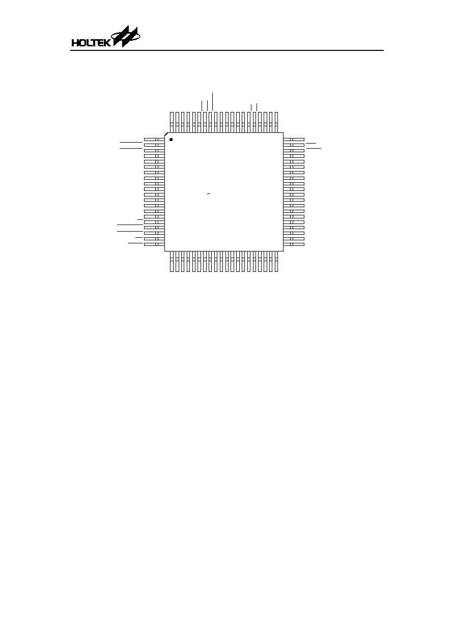
Pin Assignment
HT9580
3
April 28, 2000
Preliminary
2 1 4 0
6 0
6 1
8 0
1
2 0
4 1
H T 9 5 8 0
8 0 L Q F P
D A _ O U T
B A F
S R D Y / B A L
V S S
V D D
B Z
P C 1
P C 0
P B 7
P B 6
P B 5
P B 4
P B 3
P B 2
P B 1
P B 0
T M R 1
A 0
A 1
A 2
RS
S
I
D
I
/M
IS
O
BS
3
/
M
O
SI
BS
2
/
SC
K
BS
1/
S
S
TS
PA
5
PA
4
PA
3
PA
2
PA
1
PA
0
RE
S
E
T
TS
C
TS
1
OS
C
2
OS
C
1
VS
S
X2
X1
V D D
L C D _ C S 1
L C D _ C S 0
L C D _ C L
L C D _ A 0
L C D _ R W
L C D _ E
D 7
D 6
D 5
D 4
D 3
D 2
D 1
D 0
R / W
S R A M _ C E
M A S K _ C E
O E
P S E N
A3
A4
A5
A6
A7
A8
A9
A10
A11
A12
A13
A14
A15
VS
S
P_
M
O
D
E
VD
D
RA
14
RA
15
RA
16
RA
17
Pin Description
Pin No.
Pin Name
I/O
Description
1, 25, 56 VDD
¾
Positive power supply
2
LCD_CS1
O
LCD driver chip select control (for slave LCD driver)
3
LCD_CS0
O
LCD driver chip select control (for master LCD driver)
4
LCD_CL
O
LCD driver clock output
5
LCD_A0
O
LCD driver data/command select control
6
LCD_RW
O
LCD Driver Read/Write signal output
7
LCD_E
O
LCD driver enable clock control
15~8
D0~D7
I/O 8-bit, tristate, bidirectional I/O data bus.
16
R/W
O
Read/Write signal output
17
SRAM_CE
O
SRAM chip Enable. This signal is generated from the HT9580 to
provide read or write timing for external SRAM devices. (See Ap-
plication Circuit)
18
MASK_CE
O
Mask ROM Chip Enable. This signal is generated from the
HT9580 to provide read timing for external Mask ROM devices.
(See Application Circuit)
19
OE
O
Mask ROM or SRAM Output Enable. This signal is generated
from the HT9580 to provide read timing for external Mask ROM
and SRAM devices. (See Application Circuit)
20
PSEN
O
Program Store Enable. This pin is used to connect the OE and CE
pins of the external 44 Kbytes program ROM when the
²MODE_P² internal pad is connected to VSS. (See note)
21~24
RA17~RA14
O
Extended address bus pins
26
P_MODE
I
Internal or external program ROM selection without pull-high re-
sistor. If the pin connects to VDD, the internal program ROM will
be fetched (normal type), otherwise the external program ROM
will be fetched when the pin connects to VSS (Romless).
27, 57, 78 VSS
¾
Negative power supply
43~28
A0~A15
O
Address bus pins. This is used for memory and I/O exchanges on
the data bus.
44
TMR1
I
Schmitt trigger input for timer1 counter with pull-high resisor.
45~52
PB0~PB7
I/O General Input/Output Port B. The input cell structures can be se-
lected as CMOS or CMOS with pull-high resistors.
53~54
PC0~PC1
I/O General Input/Output Port C. The input cell structures can be se-
lected as CMOS or CMOS with pull-high resistors.
55
BZ
O
Buzzer non-inverting BZ output
HT9580
4
April 28, 2000
Preliminary
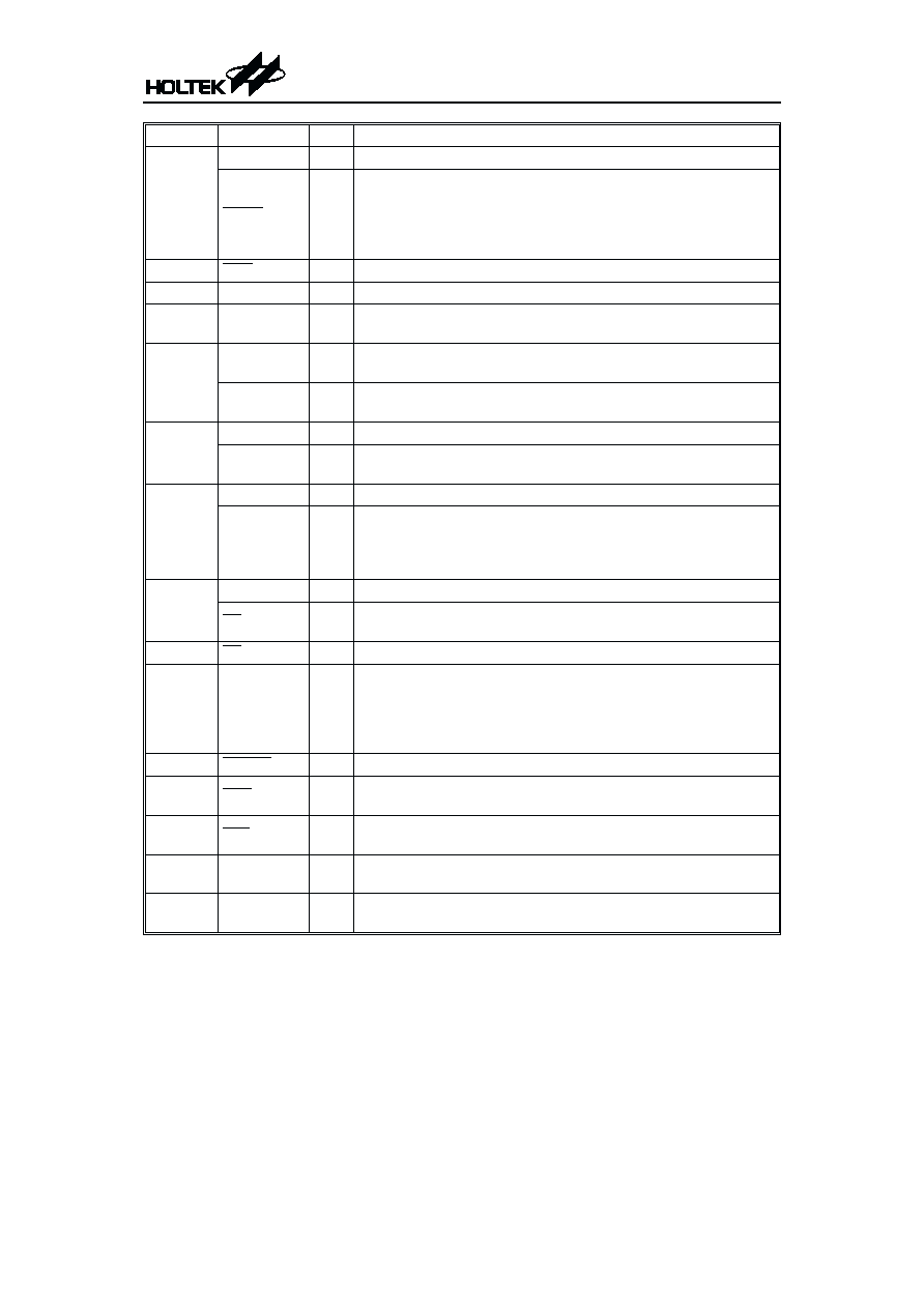
Pin No.
Pin Name
I/O
Description
58
BAL
I
Battery voltage detector input with pull-high resistor.
SRDY
I
SPI slave ready ¾ This slave ready pin is a Schmitt trigger input
with pull-high resistor. When the slave initiates the SPI transfer,
a high to low transition activates an interrupt. When the master
initiates the SPI transfer, a high to low transition trigger the
master to start the transfer.
59
BAF
I
Battery fail indication input, active low.
60
DA_OUT
O
D/A converter output. This pin is an 8-bit D/A analog output
61
RSSI
I
RSSI output from IF circuit. This pin should be pulled high or low
externally when this pin is not used.
62
DI
I
POCSAG code input serial data. CMOS input with pull-high re-
sistor.
MISO
I
SPI master-in-slave-out ¾ this is the data input with pull-high
resistor for SPI communications.
63
BS3
O
PLL power control enable, CMOS output
MOSI
O
SPI master-out-slave-in ¾ this is the data output for SPI commu-
nications.
64
BS2
O
RF quick charge control enable, CMOS output
SCK
I/O
SPI serial clock ¾ the SCK signal is used to synchronize the data
transfer. If HT9580 is in the master mode, the SCK is output
clock. Otherwise, SCK is input clock if HT9580 is in the slave
mode.
65
BS1
O
Pager receiver power control enable output, CMOS output
SS
O
SPI slave select ¾ this signal is used to enable the SPI slave for
transfer.
66
TS
I
Decoder test mode input pin, active low with pull-high resistor.
72~67
PA0~PA5
I/O
General Input/Output Port A. These ports can be programmed to
have a wake-up capability for applications in keyboard operations
or as normal I/O. Also the input cell structures are all Schmitt
trigger types and can be selected between CMOS or CMOS with
pull-high resistors.
73
RESET
I
Schmitt trigger reset input, active low.
74
TSC
I
mC test mode input pin, active low with internal pull-high resis-
tor. The test circuit will be activated when this pin pulls low.
75
TS1
I
Decoder test mode input pin, active low with pull-high resistor.
The internal test mode will be activated when this pin pulls low.
77
76
OSC1
OSC2
I
O
OSC1 and OSC2 are connected to an RC network to form a main
clock oscillator
80
79
X1
X2
I
O
X1 and X2 are connected to a crystal to form an internal low power
clock oscillator (32.768kHz, 76.8kHz, or 153.6kHz)
HT9580
5
April 28, 2000
Preliminary
Document Outline
- þÿ
- þÿ
- þÿ
- þÿ
- þÿ
- þÿ
- þÿ
- þÿ
- þÿ
- þÿ
- þÿ
- þÿ
- þÿ
- þÿ