HY51V(S)16160HG(HGL).PDF
HY51V(S)16160HG/HGL
1M x 16Bit Fast Page DRAM
This document is a general product description and is subject to change without notice. Hyundai Electronics does not assume any
responsibility for use of circuits described. No patent licenses are implied.
Rev.0.1/Apr.01
DESCRIPTION
FEATURES
·
Fast access time and cycle time
ORDERING INFORMATION
Part No
tRAC
tCAC
tRC
tPC
HY51V(S)16160HG/HGL-5
50ns
13ns
90ns
35ns
HY51V(S)16160HG/HGL-6
60ns
15ns
110ns
40ns
HY51V(S)16160HG/HGL-7
70ns
18ns
130ns
45ns
50ns
60ns
70ns
Active
396mW
360mW
324mW
Standby
7.2mW(CMOS level Max)
0.54mW (L-version : Max)
Part Number
Access Time
Package
HY51V(S)16160HGJ/HG(L)J-5
HY51V(S)16160HGJ/HG(L)J-6
HY51V(S)16160HGJ/HG(L)J-7
50ns
60ns
70ns
400mil 42pin SOJ
HY51V(S)16160HGT/HG(L)T-5
HY51V(S)16160HGT/HG(L)T-6
HY51V(S)16160HGT/HG(L)T-7
50ns
60ns
70ns
400mil 44(50)pin TSOP-II
PRELIMINARY
The HY51V(S)16160HG/HGL is the new generation dynamic RAM organized 1,048,576 words x 16bit.
HY51V(S)16160HG/HGL has realized higher density, higher performance and various functions by utiliz-
ing advanced CMOS process technology. The HY51V(S)16160HG/HGL offers Fast Page Mode as a high
speed access mode. Multiplexed address inputs permit the HY51V(S)16160HG/HGL to be packaged in
standard 400mil 42pin SOJ and 44(50) pin TSOP-II. The package size provides high system bit densities
and is compatible with widely available automated testing and insertion equipment.
System oriented features include single power supply 3.3V +/- 0.3V tolerance, direct interfacing capability
with high performance logic families such as Schottky TTL.
·
Fast Page Mode capability
·
Read-modify-write capability
·
Multi-bit parallel test capability
·
TTL(3.3V) compatible inputs and outputs
·
/RAS only, CAS-before-/RAS, Hidden and self
refresh(L-version) capability
·
JEDEC standard pinout
·
42pin plastic SOJ/44(50)pin TSOP-II(400mil)
·
Single power supply of 3.3V +/- 0.3V
·
Battery back up operation(L-version)
·
2 /CAS byte control
·
Power dissipation
·
Refresh cycle
Part No
Ref
Normal
L-part
HY51V16160HG
4K
64ms
HY51V16160HGL
4K
128ms
(S) : Self refresh, (L) : Low power
HY51V(S)16160HG/HGL
Rev.0.1/Apr.01
2
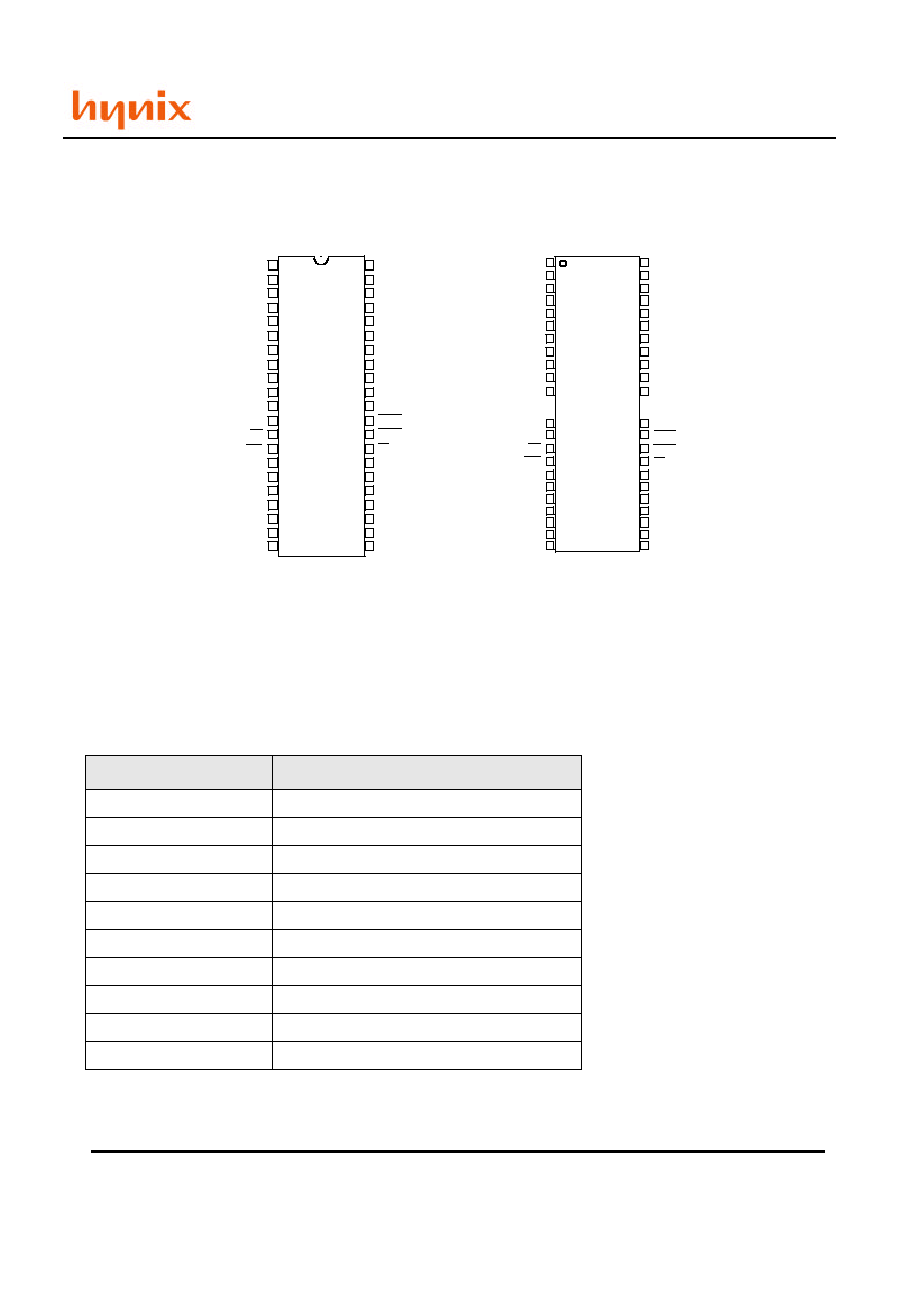
PIN CONFIGURATION
Pin
Function
/RAS
Row Address Strobe
/UCAS, /LCAS
Column Address Strobe
/WE
Write Enable
/OE
Output Enable
A0-A11
Address Inputs
A0-A11
Refresh Address Inputs
I/O 0- I/O15
Data Input / Output
Vcc
Power (3.3V)
Vss
Ground
NC
No connection
PIN DESCRIPTION
42
43
44
45
46
40
41
33
30
31
32
27
28
29
26
34
35
36
47
48
49
50
NC
NC
V
SS
I/O15
I/O14
I/O13
I/O12
I/O11
I/O10
I/O9
I/O8
V
SS
LCAS
UCAS
OE
A8
A7
A6
A5
A4
V
SS
A9
V
SS
I/O15
I/O14
I/O13
I/O12
38
39
40
41
42
I/O11
I/O10
I/O9
I/O8
NC
32
33
34
35
36
V
SS
37
LCAS
UCAS
OE
29
30
31
A9
A8
A7
26
27
28
A6
A5
A4
23
24
25
V
SS
22
11
1
2
3
4
5
7
8
9
10
6
15
16
17
18
19
20
21
22
23
24
25
NC
NC
I/O0
I/O1
I/O2
I/O3
I/O4
I/O5
I/O6
I/O7
V
CC
NC
WE
RAS
A11
A10
A0
A1
V
CC
V
CC
A2
A3
V
CC
I/O0
I/O1
I/O2
I/O3
1
2
3
4
5
I/O4
I/O5
I/O6
I/O7
NC
7
8
9
10
11
V
CC
6
NC
WE
RAS
12
13
14
A11
A10
A0
15
16
17
A1
A2
A3
18
19
20
V
CC
21
42 Pin Plastic SOJ
44(50) Pin Plastic TSOP-II
HY51V(S)16160HG/HGL
Rev.0.1/Apr.01
3
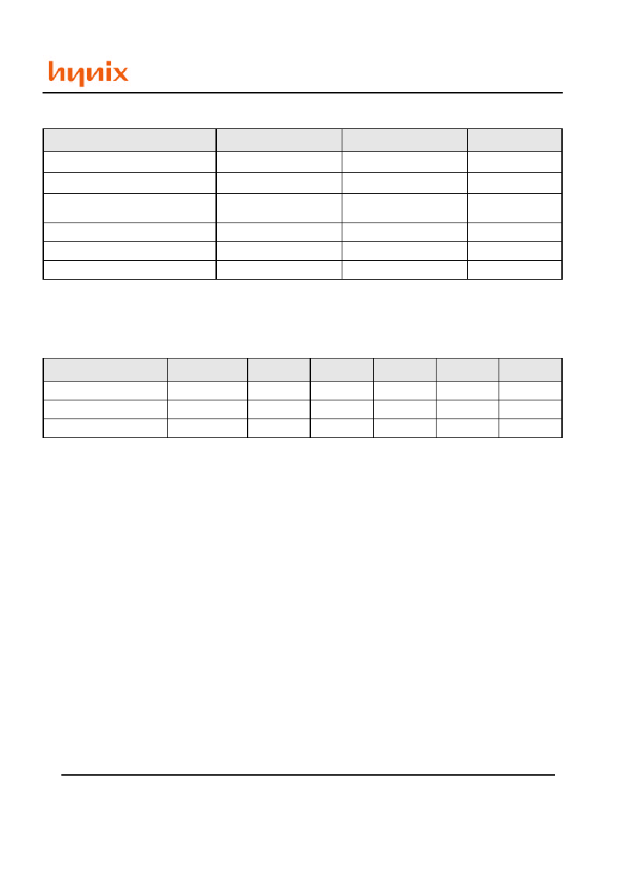
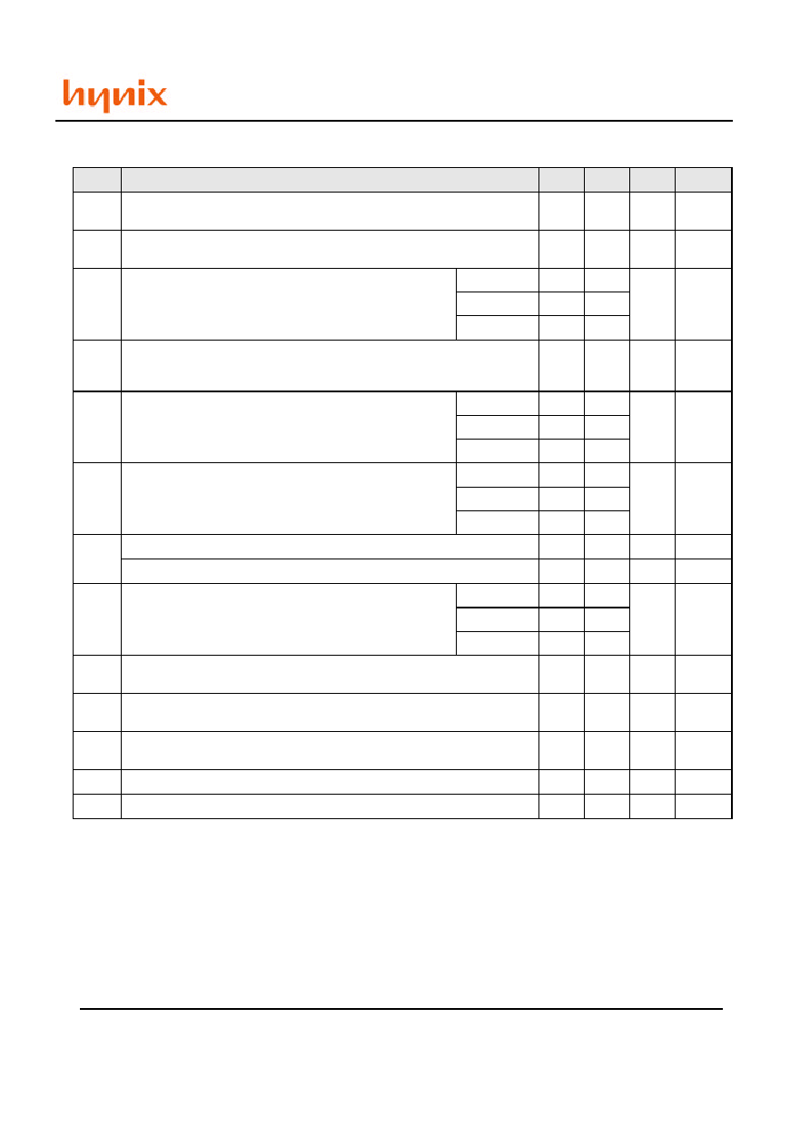
ABSOLUTE MAXIMUM RATINGS
Recommended DC OPERATING CONDITIONS
(TA=0 to 70
o
C)
Note : All voltages are referenced to Vss
Parameter
Symbol
Rating
Unit
Ambient Temperature
T
A
0 ~ 70
o
C
Storage Temperature
T
STG
-55 ~ 125
o
C
Voltage on Any Pin relative to V
ss
V
T
-0.5 ~ Vcc + 0.5
(Max 4.6V)
V
Voltage on V
cc
relative to V
ss
V
cc
-0.5 ~ 4.6
V
Short Circuit Output Current
I
OUT
50
mA
Power Dissipation
P
T
1
W
Parameter
Symbol
Min
Typ.
Max
Unit
Note
Power Supply Voltage
V
cc
3.0
3.3
3.6
V
Input High Voltage
V
IH
2.0
-
V
cc
+ 0.3
V
Input Low Voltage
V
IL
-0.3
-
0.8
V
HY51V(S)16160HG/HGL
Rev.0.1/Apr.01
4
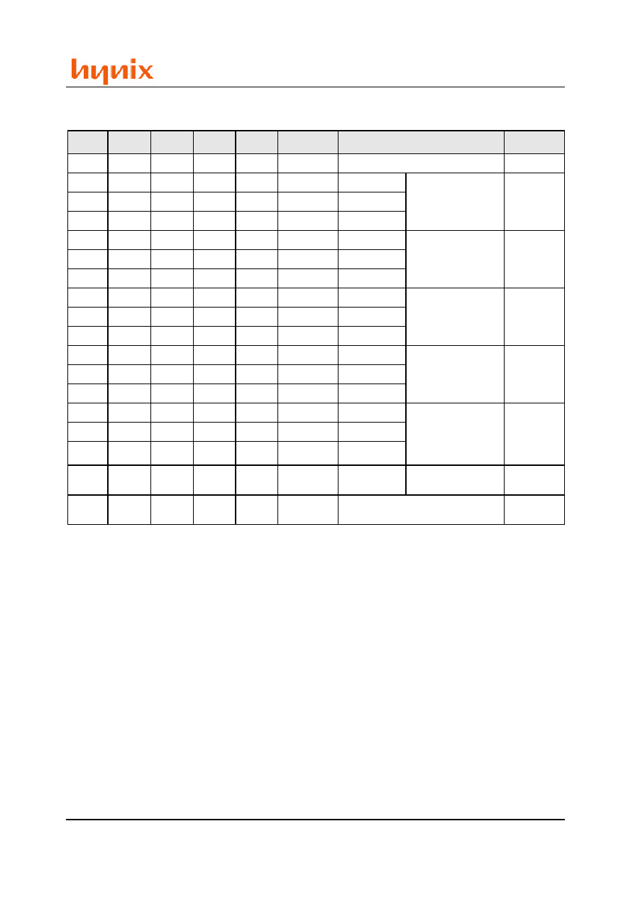
Truth Table
Notes :
1. H : High ( inactive) L : Low ( active) D : H or L
2. t
WCS
>= 0ns Early write cycle
twcs <
=0
ns Delayed write cycle
3. Mode is determined by the OR function of the /UCAS and /LCAS (mode is set by earliest of /UCAS and /LCAS
active edge and reset by the latest of /UCAS and /LCAS inactive edge), However write operation and output
High-Z control are done independently by each /UCAS, /LCAS
ex) if /RAS = H to L, /UCAS = H, /LCAS = L, then /CAS-before-/RAS refresh cycle is selected
/RAS
/LCAS
/UCAS
/WE
/OE
Output
Operation
Notes
H
D
D
D
D
Open
Standby
1 ,3
L
L
H
H
L
Valid
Lower byte
Read cycle
1, 3
L
H
L
H
L
Valid
Upper byte
L
L
L
H
L
Valid
Word
L
L
H
L
D
Open
Lower byte
Early write cycle
1, 2, 3
L
H
L
L
D
Open
Upper byte
L
L
L
L
D
Open
Word
L
L
H
L
H
Undefined
Lower byte
Delayed write cycle
1, 2, 3
L
H
L
L
H
Undefined
Upper byte
L
L
L
L
H
Undefined
Word
L
L
H
H to L
L to H
Valid
Lower byte
Read-modify-write
Cycle
1, 3
L
H
L
H to L
L to H
Valid
Upper byte
L
L
L
H to L
L to H
Valid
Word
H to L
H
L
D
D
Open
Word
CBR refresh
or
Self refresh
(L-series)
1, 3
H to L
L
H
D
D
Open
Word
H to L
L
L
D
D
Open
Word
L
H
H
D
D
Open
Word
/RAS only refresh
cycle
1, 3
L
L
L
H
H
Open
Read cycle
(Output disabled)
1, 3
HY51V(S)16160HG/HGL
Rev.0.1/Apr.01
5
DC CHARACTERISTICS
(Vcc = 3.3V +/- 10%, TA=0 to 70
°
C
)
Note :
1. Icc depends on output load condition when the device is selected, Icc(max) is specified at the output open condition
2. Address can be changed once or less while /RAS=VIL
3. Address can be changed once or less while /UCAS and /LCAS =VIH
4. /UCAS = L (<=0.2) and /LCAS=L (<=0.2) while /RAS=L (<=0.2)
5. L-Version
Symbol
Parameter
Min
Max
Unit
Note
VOH
Output Level
Output Level voltage(Iout= -2mA)
2.4
Vcc
V
VOL
Output Level
Output Level voltage(Iout=2mA)
0
0.4
V
ICC1
Operating current
Average power supply operating current
( /RAS, /CAS Cycling : tRC = tRC min)
50ns
-
110
mA
1, 2
60ns
-
100
70ns
-
90
I
CC2
Standby current (TTL interface)
Power supply standby current
(/RAS, /CAS=VIH, Dout = High-Z)
-
2
mA
ICC3
/RAS only refresh current
Average power supply current
/RAS only refresh mode
(tRC= tRC min)
50ns
-
110
mA
2
60ns
-
100
70ns
-
90
ICC4
Fast page mode current
Average power supply current
Fast page mode (tPC=tPC min)
50ns
-
115
mA
1, 3
60ns
-
105
70ns
-
95
ICC5
CMOS interface ( /RAS, /CAS >= Vcc-0.2V, Dout = High-Z)
-
1
mA
Standby current ( L-version)
-
150
uA
4
ICC6
/CAS-before-/RAS refresh current (tRC=tRC min)
50ns
-
110
mA
60ns
-
100
70ns
-
90
ICC7
Battery back up operating current (standby with CBR refresh)
(tRC=31.3us, tRAS<=0.3us, Dout=High-Z)
-
400
uA
4
ICC8
Standby current
( /RAS = VIH, /CAS = VIL, Dout=Enable)
-
5
uA
1
ICC9
Self refresh current
(/RAS, /CAS <=0.2V, Dout=High-Z, CMOS interface)
-
250
uA
4
II(L)
Input leakage current, Any input (0V<= Vin<=4.6V)
-10
10
uA
IO(L)
Output leakage current, (Dout is disabled, 0V<= Vout<=4.6V)
-10
10
uA