FEATURES
·
High-speed access time: 8, 9, 10, 12 ns
·
CMOS low power operation
--
720 mW (typical) operating @ 9 ns
--
36 mW (typical) standby @ 9 ns
·
TTL compatible interface levels
·
Single 3.3V power supply
·
Fully static operation: no clock or refresh
required
·
Three state outputs
·
Available in 119-pin 14x22mm PBGA
DESCRIPTION
The
ICSI
IS61LV12824 is a high-speed, static RAM organized
as 131,072 words by 24 bits. It is fabricated using
ICSI
's high-
performance CMOS technology. This highly reliable process
coupled with innovative circuit design techniques, yields ac-
cess times as fast as 8 ns with low power consumption.
When
CE1, CE2 are HIGH and CE2 is LOW (deselected), the
device assumes a standby mode at which the power dissipa-
tion can be reduced down with CMOS input levels.
Easy memory expansion is provided by using Chip Enable and
Output Enable inputs,
CE1, CE2, CE2 and OE. The active
LOW Write Enable (
WE) controls both writing and reading of
the memory.
The IS61LV12824 is packaged in the JEDEC standard
119-pin 14*22mm PBGA.
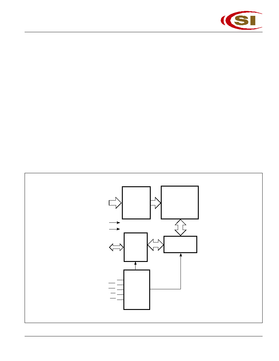
FUNCTIONAL BLOCK DIAGRAM
ICSI reserves the right to make changes to its products at any time without notice in order to improve design and supply the best possible product. We assume no responsibility for any errors
which may appear in this publication. © Copyright 2000, Integrated Circuit Solution Inc.
A0-A16
CE1
OE
WE
128K x 24
MEMORY ARRAY
DECODER
COLUMN I/O
CONTROL
CIRCUIT
GND
VCC
I/O
DATA
CIRCUIT
CE2
CE2
I/O0-I/O23
IS61LV12824
128K x 24 HIGH-SPEED CMOS STATIC RAM
WITH 3.3V SUPPLY
Integrated Circuit Solution Inc.
1
SR021-0B
IS61LV12824
128K x 24 HIGH-SPEED CMOS STATIC RAM
WITH 3.3V SUPPLY
IS61LV12824
Integrated Circuit Solution Inc.
3
SR021-0B
1
2
3
4
5
6
7
8
9
10
11
12
OPERATING RANGE
Range
Ambient Temperature
V
CC
(8, 9, 10 ns)
V
CC
(12 ns)
Commercial
0°C to +70°C
3.3V + 10%, 5%
3.3V ± 10%
Industrial
40°C to +85°C
3.3V + 10%, 5%
3.3V ± 10%
DC ELECTRICAL CHARACTERISTICS
(Over Operating Range)
Symbol
Parameter
Test Conditions
Min.
Max.
Unit
V
OH
Output HIGH Voltage
V
CC
= Min., I
OH
= 4.0 mA
2.4
--
V
V
OL
Output LOW Voltage
V
CC
= Min., I
OL
= 8.0 mA
--
0.4
V
V
IH
Input HIGH Voltage
2.2
V
CC
+ 0.3
V
V
IL
Input LOW Voltage
(1)
0.3
0.8
V
I
LI
Input Leakage
GND
V
IN
V
CC
1
1
µA
I
LO
Output Leakage
GND
V
OUT
V
CC
, Outputs Disabled
1
1
µA
Note:
1.
V
IL
(min.) = 0.3V DC; V
IL
(min.) = 2.0V AC (pulse width
2.0 ns).
V
IH
(max.) = V
CC
+ 0.3V DC; V
IH
(max.) = V
CC
+ 2.0V AC (pulse width
2.0 ns).
ABSOLUTE MAXIMUM RATINGS
(1)
Symbol
Parameter
Value
Unit
V
CC
Power Supply Voltage Relative to GND
0.5 to 5.0
V
V
TERM
Terminal Voltage with Respect to GND
0.5 to Vcc + 0.5
V
T
STG
Storage Temperature
65 to + 150
°C
T
BIAS
Temperature Under Bias:
Com.
10 to + 85
°C
Ind.
45 to + 90
°C
P
T
Power Dissipation
2.0
W
I
OUT
DC Output Current
±20
mA
Note:
1.
Stress greater than those listed under ABSOLUTE MAXIMUM RATINGS may cause permanent
damage to the device. This is a stress rating only and functional operation of the device at these or
any other conditions above those indicated in the operational sections of this specification is not
implied. Exposure to absolute maximum rating conditions for extended periods may affect reliability.
TRUTH TABLE
Mode
WE
WE
WE
WE
WE
CE1
CE1
CE1
CE1
CE1
CE2
CE2
CE2
CE2
CE2
CE2
OE
OE
OE
OE
OE
I/O0-I/O23
Vcc Current
Not Selected
X
H
X
X
X
High-Z
I
SB
1
, I
SB
2
Output Disabled
H
L
H
L
H
High-Z
I
CC
X
L
H
L
X
High-Z
Read
H
L
H
L
L
D
OUT
1
CC
H
L
H
L
H
High-Z
Write
L
L
H
L
X
D
IN
I
CC
L
L
H
L
H
H
IHG
-Z
IS61LV12824
4
Integrated Circuit Solution Inc.
SR021-0B
CAPACITANCE
(1)
Symbol
Parameter
Conditions
Max.
Unit
C
IN
Input Capacitance
V
IN
= 0V
6
pF
C
OUT
Input/Output Capacitance
V
OUT
= 0V
8
pF
Note:
1.
Tested initially and after any design or process changes that may affect these parameters.
POWER SUPPLY CHARACTERISTICS
(1)
(Over Operating Range)
-8 ns
-9 ns
-10 ns
-12 ns
Symbol Parameter
Test Conditions
Min. Max.
Min. Max.
Min. Max.
Min. Max.
Unit
I
CC
Vcc Dynamic Operating
V
CC
= Max.,
Com.
--
210
--
200
--
180
--
190
mA
Supply Current
I
OUT
= 0 mA, f = f
MAX
Ind.
--
--
--
220
--
210
--
190
I
SB
1
TTL Standby Current
V
CC
= Max.,
Com.
--
70
--
60
--
50
--
50
mA
(TTL Inputs)
V
IN
= V
IH
or V
IL
, f = 0
Ind.
--
70
--
70
--
55
--
55
CE1, CE2,
V
IH
, CE2
V
IL
I
SB
2
CMOS Standby
V
CC
= Max.,
Com.
--
10
--
10
--
10
--
10
mA
Current (CMOS Inputs)
CE1, CE2
V
CC
0.2V,
Ind.
--
--
--
20
--
20
--
20
CE2
0.2V, V
IN
V
CC
0.2V,
or V
IN
0.2V, f = 0
Note:
1.
At f = f
MAX
, address and data inputs are cycling at the maximum frequency, f = 0 means no input lines change.
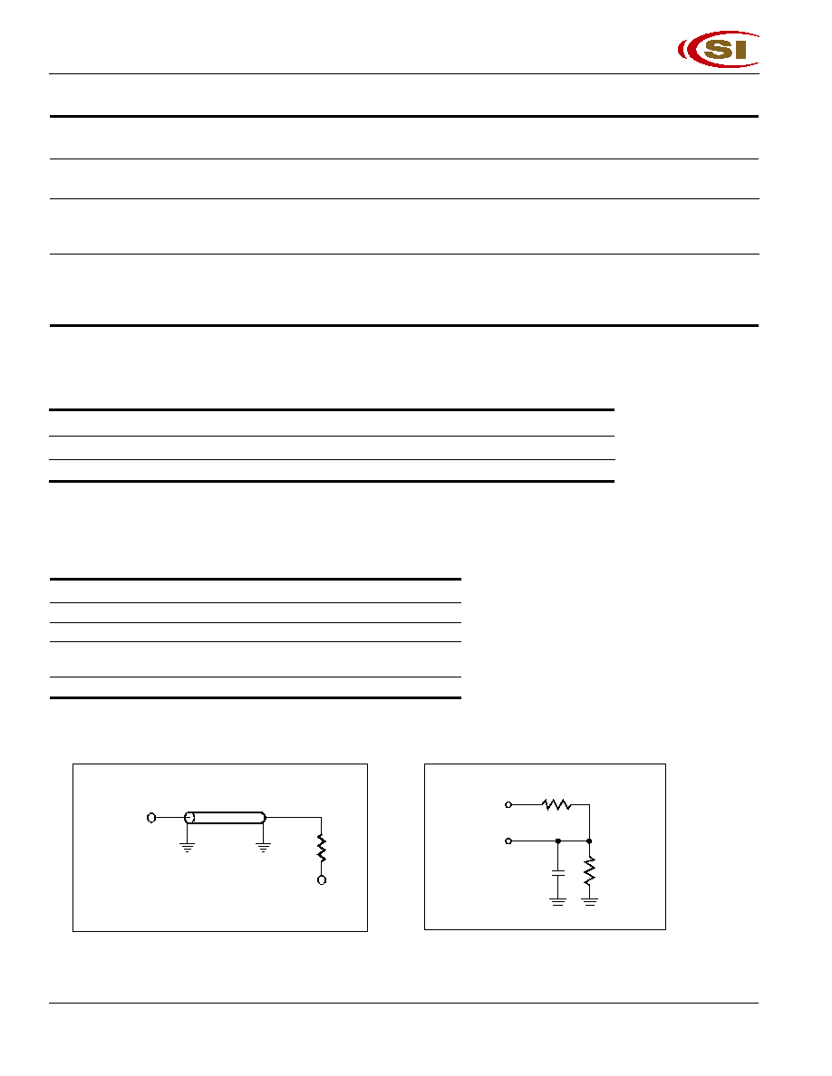
AC TEST CONDITIONS
Parameter
Unit
Input Pulse Level
0V to 3.0V
Input Rise and Fall Times
2 ns
Input and Output Timing
1.5V
and Reference Level
Output Load
See Figures 1 and 2
AC TEST LOADS
Figure 1
Figure 2
319
5 pF
Including
jig and
scope
353
OUTPUT
3.3V
OUTPUT
Z
O
= 50
1.5V
50
IS61LV12824
Integrated Circuit Solution Inc.
5
SR021-0B
1
2
3
4
5
6
7
8
9
10
11
12
READ CYCLE SWITCHING CHARACTERISTICS
(1)
(Over Operating Range)
-8
-9
-10
-12
Symbol Parameter
Min. Max.
Min. Max.
Min.
Max.
Min. Max.
Unit
t
RC
Read Cycle Time
9
--
10
--
12
--
15
--
ns
t
AA
Address Access Time
--
9
--
10
--
12
--
15
ns
t
OHA
Output Hold Time
3
--
3
--
3
--
3
--
ns
t
ACE
CE1, CE2 Access Time
--
8
--
9
--
10
--
12
ns
t
ACE
2
CE2 Access Time
t
DOE
OE Access Time
--
4
--
4
--
4
--
4
ns
t
HZOE
(2)
OE to High-Z Output
0
5
0
5
0
6
0
7
ns
t
LZOE
(2)
OE to Low-Z Output
0
--
0
--
0
--
0
--
ns
t
HZCE
(2)
CE1, CE2 to High-Z Output
0
5
0
5
0
6
0
7
ns
t
HZCE
2
(2)
CE2 to High-Z Output
t
LZCE
(2)
CE, CE2 to Low-Z Output
3
--
3
--
3
--
3
--
ns
t
LZCE
2
(2)
CE2 to Low-Z Output
Notes:
1.
Test conditions assume signal transition times of 2 ns or less, timing reference levels of 1.5V, input pulse levels of 0 to 3.0V
and output loading specified in Figure 1.
2.
Tested with the load in Figure 2. Transition is measured ±200 mV from steady-state voltage. Not 100% tested.