
IS61NW6432
Integrated Circuit Solution Inc.
1
SSR006-0B
ICSI reserves the right to make changes to its products at any time without notice in order to improve design and supply the best possible product. We assume no responsibility for any errors
which may appear in this publication. © Copyright 2000, Integrated Circuit Solution Inc.
FEATURES
Fast access time:
5 ns-100 MHz; 6 ns-83 MHz;
7 ns-75 MHz; 8ns-66 MHz;
No wait cycles between Read and write
Internal self-timed write cycle
Individual byte write Control
Clock controlled, registered address, data and
control
Pentium
TM
or Inear burst sequence control using
MODE input
Three chip enables for simple depth depth
expansion and adress pipelining
Common data inputs and data outputs
JEDEC 100-pin LQFP and PQFP package
Single+3.3V power supply
Optional data strobe pin (#80) for latching data
(See page 12 for detailed timing)
DESCRIPTION
The IS61NW6432 is a high-speed, low-power synchronous
static RAM designed to provide a burstable, high-performance,
no-wait bus, secondary cache for the Pentium, 680X0, and
Power PC microprocessors. It is organized as 65,536 words
by 32 bits, fabricated with ICSI's advanced CMOS technology.
Incorporating a no-wait bus, wait cycles are eliminated when
the bus switches from read to write, or write to read. This
device integrates a 2-bit burst counter, high-speed SRAM
core, and high-drive capability outputs into a single monolithic
circuit.
All synchronous inputs pass through registers controlled by a
Positive-edge-trggered clock input. Operations may be sus-
pended and all synchronous inputs ignored when Clock Enable,
CEN is HIGH. In this state the internal device will hold their
previous values.
When the ADV/LD is HIGH the internal burst counter is
incremented. New external addresses can be loaded when
ADV/LD is LOW.
Write cycles are internally self-timed and are initiated by the
rising edge of the clock inputs and when RD/WE is LOW.
Separate byte enables allow indiviual bytes to be written. BW1
controls I/O1-I/P8; BW2 controls I/O9-I/O16;BW3 controls I/
O17-I/O24; BW4 controls I/O25-I/O32. All Bytes are written
when BW1, BW2, BW3, and BW4 are LOW.
MODE pin upon power up is in interleave burst mode. It can be
connected to GND or Vcc
Q
to alter power up state.
IS61NW6432
64K x 32 SYNCHRONOUS STATIC RAM
WITH NO-WAIT STATE BUS FEATURE

IS61NW6432
2
Integrated Circuit Solution Inc.
SSR006-0B
BLOCK DIAGRAM

IS61NW6432
Integrated Circuit Solution Inc.
3
SSR006-0B
PIN CONFIGURATION
100-Pin LQFP and PQFP (Top View)
NC
I/O16
I/O15
VCCQ
GNDQ
I/O14
I/O13
I/O12
I/O11
GNDQ
VCCQ
I/O10
I/O9
GND
VCC
VCC
GND
I/O8
I/O7
VCCQ
GNDQ
I/O6
I/O5
I/O4
I/O3
GNDQ
VCCQ
I/O2
I/O1
NC
A6
A7
CE1
CE2
BW4
BW3
BW2
BW1
CE3
VCC
GND
CLK
R/W
CEN
OE
ADV/LD
NC
NC
A8
A9
NC
I/O17
I/O18
VCCQ
GNDQ
I/O19
I/O20
I/O21
I/O22
GNDQ
VCCQ
I/O23
I/O24
VCC
VCC
VCC
GND
I/O25
I/O26
VCCQ
GNDQ
I/O27
I/O28
I/O29
I/O30
GNDQ
VCCQ
I/O31
I/O32
NC
1
2
3
4
5
6
7
8
9
10
11
12
13
14
15
16
17
18
19
20
21
22
23
24
25
26
27
28
29
30
80
79
78
77
76
75
74
73
72
71
70
69
68
67
66
65
64
63
62
61
60
59
58
57
56
55
54
53
52
51
100 99 98 97 96 95 94 93 92 91 90 89 88 87 86 85 84 83 82 81
31 32 33 34 35 36 37 38 39 40 41 42 43 44 45
MODE
A5
A4
A3
A2
A1
A0
NC
NC
GND
VCC
NC
NC
A10
A11
A12
A13
A14
A15
NC
46 47 48 49 50
PIN DESCRIPTIONS
A0-A15
Address Inputs
CLK
Clock
CEN
Clock Enale
ADV/CD
Advance Load
BW1-BW4
Synchronous Byte Write Enable
R / W
Read / Write
CE1, CE2, CE3
Synchronous Chip Enable
OE
Output Enable
DS
Data Strobe
Notes:
1. Optional, NC or DS.
I/O-I/O32
Data Input/Output
MODE
Burst Sequence Mode
V
CC
+3.3V Power Supply
GND
Ground
V
CCQ
Isolated Output Buffer Supply:
+3.3V
GND
Q
Isolated Output Buffer Ground
NC
No Connect
IS61NW6432
4
Integrated Circuit Solution Inc.
SSR006-0B
TRUTH TABLE
(1)
Address
Operation
Used
R/W
/W
/W
/W
/W
CEx
CEx
CEx
CEx
CEx
ADV/LD
/LD
/LD
/LD
/LD
CEN
CEN
CEN
CEN
CEN
BW
BW
BW
BW
BWx
CLK
Bein New Write Cycle
External
L
L
L
L
Valid
L-H
Begin New Read Cycle
External
H
L
L
L
X
L-H
Advance Burst Counter
Internal
X
X
H
L
Valid
L-H
(Burst Write)
Advance Burst Counter
Internal
X
X
H
L
X
L-H
(BurstRead)
Deselect (2 Cycle)
X
X
H
L
L
X
L-H
Hold/NOOP
"
X
X
X
X
H
X
L-H
Notes:
1. "X" Means don't care.
2. When ADV/LD signal is sampled HI|GH, the internal burst counter is incremented. The R/W signal is ignored when the counter
is advanced, Therefore, the nature of the burst cycle (Read or Write) is deternined by the status of the R/W signal when the
first address is loaded at the beginning of the burst cycle.
3. Deselect cycle is initiated when CEx is sampled HIGH and ADV/LD sampled LOW at rising edge of clock. The data bus will
tristate two cycles after deselect is initiated.
4. When CEN is sampled high at the rising edge of clock, that clock edge is blocked form propogating through the part. The state
of all the internal registers remains unchanged.
PARTIAL TRUTH TABLE(Non-burst)
Function
GW
GW
GW
GW
GW
BW1
BW1
BW1
BW1
BW1
BW2
BW2
BW2
BW2
BW2 BW3
BW3
BW3
BW3
BW3 BW4
BW4
BW4
BW4
BW4
CEx
CEx
CEx
CEx
CEx ADV/LD
/LD
/LD
/LD
/LD
READ
H
X
X
X
X
L
L
WRITE Byte 1
L
L
H
H
H
L
L
WRITE Byte 2
L
H
L
H
H
L
L
WRITE Byte 3
L
H
H
L
H
L
L
WRITE Byte 4
L
H
H
H
L
L
L
WRITE All Bytes
L
L
L
L
L
X
L
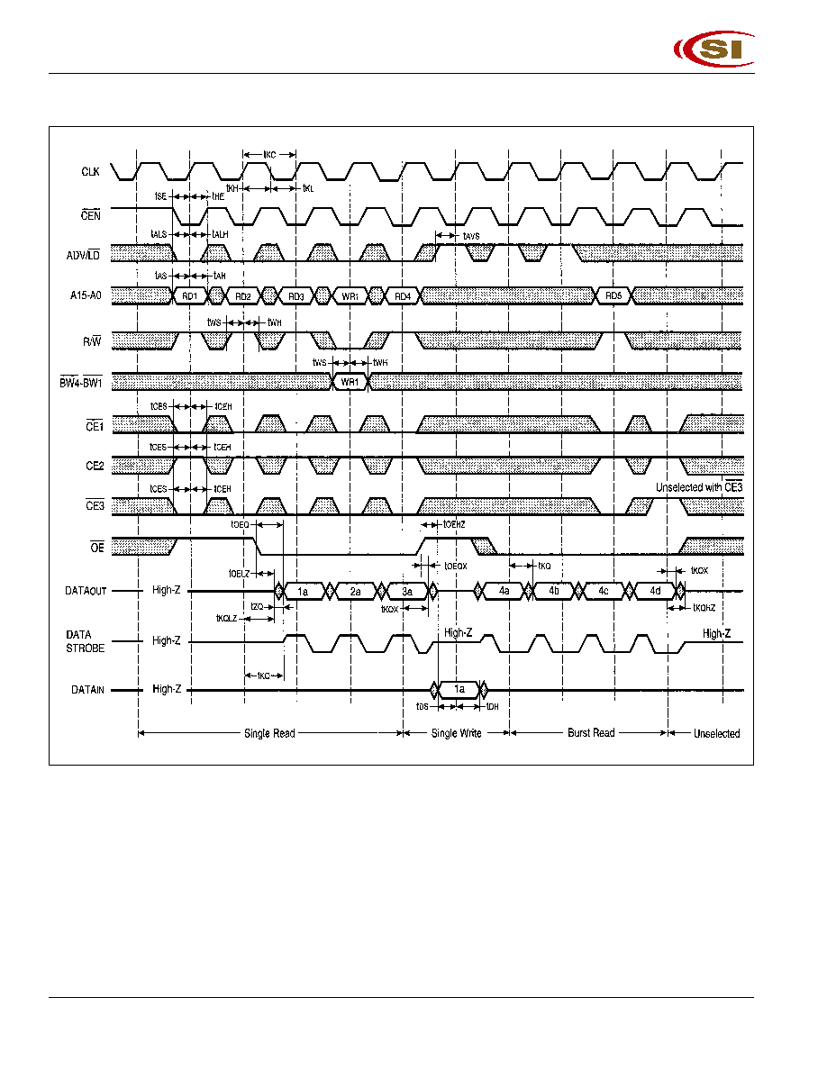
FUNCTIONAL TIMING DIAGRAM

IS61NW6432
Integrated Circuit Solution Inc.
5
SSR006-0B
TYPICAL OPERATION
CE1, CE3 and CEN are LOW, CE2 is HIGH, Non-Burst Operation
Cycle
Address
R/W
R/W
R/W
R/W
R/W
ADV/LD
CEX
CEX
CEX
CEX
CEX
CEN
CEN
CEN
CEN
CEN
BWX
BWX
BWX
BWX
BWX
OE
OE
OE
OE
OE
I/O
Comments
n
A0
H
L
L
L
X
?
D-2
?
n+1
A
1
L
L
L
L
L
?
D-1
?
n+2
A2
H
L
L
L
X
L
D0
Data Out
n+3
A3
L
L
L
L
L
X
D1
Data In
n+4
A4
H
L
L
L
X
L
D2
Data Out
n+5
A5
L
L
L
L
L
X
D3
Data In
n+6
A6
H
L
L
L
X
L
D4
Data Out
n+7
A7
L
L
L
L
L
X
D5
Data In
n+8
A8
H
L
L
L
X
L
D6
Data Out
n+9
A9
L
L
L
L
L
X
D7
Data In
n+10
A10
H
L
L
L
X
L
D8
Data Out
n+11
A11
H
L
L
L
X
X
D9
Data In
n+12
A12
L
L
L
L
L
L
D10
Data Out
n+13
A13
L
L
L
L
L
L
D11
Data Out
n+14
A14
H
L
L
L
X
X
D12
Data In
n+15
A15
H
L
L
L
X
X
D13
Data In
n+16
A16
H
L
L
L
X
L
D14
Data Out
n+17
A17
L
L
L
L
L
L
D15
Data Out
n+18
A18
L
L
L
L
L
L
D16
Data Out
n+19
A19
L
L
L
L
L
x
D17
Data In
n+20
A20
H
L
L
L
X
X
D18
Data In
n+21
A21
H
L
L
L
X
X
D19
Data In
Notes:
1. H=High; L=Low; X=Don't Care;?=Don't Know; Z=High lmpedance

IS61NW6432
6
Integrated Circuit Solution Inc.
SSR006-0B
READ OPERATION
Cycle Address R/W
R/W
R/W
R/W
R/W
ADV/LD
LD
LD
LD
LD
CEX
CEX
CEX
CEX
CEX
CEN
CEN
CEN
CEN
CEN
BWX
BWX
BWX
BWX
BWX
OE
OE
OE
OE
OE
I/O
Comments
n
A0
H
L
L
X
X
X
X
Address and Control meet setup
n+1
X
X
X
L
L
X
X
X
Clock Setup valid
n+2
X
X
X
X
X
X
L
D0
Contents of Address A0 Read Out
BURST READ OPERATION
Cycle Address R/W
R/W
R/W
R/W
R/W
ADV/LD
LD
LD
LD
LD
CEX
CEX
CEX
CEX
CEX
CEN
CEN
CEN
CEN
CEN
BWX
BWX
BWX
BWX
BWX
OE
OE
OE
OE
OE
I/O
Comments
n
A0
H
L
L
X
X
X
X
Address and Control meet setup
n+1
X
X
H
X
L
X
X
X
Clock Setup valid, Advance Counter
n+2
X
X
H
X
L
X
L
D0
Address A0 Read Out, Inc. Count
n+3
X
X
H
X
L
X
L
D0+1
Address A0+1 Read Out, Inc. Count
n+4
X
X
H
X
L
X
L
D0+2
Address A0+2 Read Out, Inc. Count
n+5
A1
H
L
L
L
X
L
D0+3
Address A0+3 Read Out, Load A1
n+6
X
X
H
X
L
X
L
D0
Address A0 Read Out, Inc. Count
n+7
X
X
H
X
L
X
L
D1
Address A1 Read Out, Inc. Count
n+8
A2
H
L
L
L
X
L
D0+1
Address A0+1 Read Out, Load A2
WRITE OPERATION
Cycle Address R/W
R/W
R/W
R/W
R/W
ADV/LD
LD
LD
LD
LD
CEX
CEX
CEX
CEX
CEX
CEN
CEN
CEN
CEN
CEN
BWX
BWX
BWX
BWX
BWX
OE
OE
OE
OE
OE
I/O
Comments
n
A0
L
L
L
L
L
X
X
Address and Control meet setup
n+1
X
X
X
L
L
X
X
X
Clock Setup valid
n+2
X
X
X
X
L
X
X
D0
Write D0 to Address A0
BURST WRITE OPERATION
Cycle Address R/W
R/W
R/W
R/W
R/W
ADV/LD
LD
LD
LD
LD
CEX
CEX
CEX
CEX
CEX
CEN
CEN
CEN
CEN
CEN
BWX
BWX
BWX
BWX
BWX
OE
OE
OE
OE
OE
I/O
Comments
n
A0
H
L
L
L
L
X
X
Address and Control meet setup
n+1
X
X
H
X
L
L
X
X
Clock Setup valid, Inc. Count
n+2
X
X
H
X
L
L
X
D0
Address A0 Write Out, Inc. Count
n+3
X
H
H
L
L
X
L
D0+1
Address A0+1 Write Out, Inc. Count
n+4
X
X
H
X
L
L
X
D0+2
Address A0+2 Write Out, Inc. Count
n+5
A1
L
L
L
L
L
X
D0+3
Address A0+3 Write Out, Load A1
n+6
X
X
H
X
L
L
X
D0
Address A0 Write Out, Inc. Count
n+7
X
X
H
X
L
L
X
D1
Address A1 Write Out, Inc. Count
n+8
A2
L
L
L
L
L
X
D0+1
Address A0+1 Write Out, Load A2
Notes:
1. H=High; L=Low; X=Don't Care;?=Don't Know; Z=High lmpedance
IS61NW6432
Integrated Circuit Solution Inc.
7
SSR006-0B
READ OPERATION WITH CLOCK ENABLE USED
Cycle Address R/W
R/W
R/W
R/W
R/W
ADV/LD
LD
LD
LD
LD
CEX
CEX
CEX
CEX
CEX
CEN
CEN
CEN
CEN
CEN
BWX
BWX
BWX
BWX
BWX
OE
OE
OE
OE
OE
I/O
Comments
n
A0
H
L
L
L
X
X
X
Address and Control meet setup
n+1
X
X
X
X
H
X
X
X
Clock n+1 lgnored
n+2
A1
H
L
L
L
X
X
X
Clock Valid
n+3
X
X
X
X
H
X
L
D0
Clock lgnored, Data D0 is on the bus
n+4
X
X
X
X
H
X
L
D0
Clock lgnored, Data D0 is on the bus
n+5
A2
H
L
L
L
X
L
D0
Address A0 Read Out (bus trans.)
n+6
A3
?
L
L
L
X
L
D1
Address A1 Read Out (bus trans.)
n+7
A4
?
L
L
L
X
L
D2
Address A2 Read Out (bus trans.)
READ OPERATION WITH CLOCK ENABLE USED
Cycle Address R/W
R/W
R/W
R/W
R/W
ADV/LD
LD
LD
LD
LD
CEX
CEX
CEX
CEX
CEX
CEN
CEN
CEN
CEN
CEN
BWX
BWX
BWX
BWX
BWX
OE
OE
OE
OE
OE
I/O
Comments
n
A0
L
L
L
L
L
X
X
Address and Control meet setup
n+1
X
X
X
X
H
X
X
X
Clock n+1 lgnored
n+2
A1
L
L
L
L
L
X
X
Clock Valid
n+3
X
X
X
X
H
X
L
di
Clock lgnored.
n+4
X
X
X
X
H
X
L
di
Clock lgnored.
n+5
A2
L
L
L
L
L
L
D0
Write data D0 (bus trans.)
n+6
A3
?
L
L
L
L
L
D1
Write data D1 (bus trans.)
n+7
A4
?
L
L
L
L
L
D2
Write data D2 (bus trans.)
Notes:
1. H=High; L=Low; X=Don't Care;?=Don't Know; Z=High lmpedance
IS61NW6432
8
Integrated Circuit Solution Inc.
SSR006-0B
ABSOLUTE MAXIMUM RATINGS
(1)
Symbol
Parameter
Value
Unit
T
BIAS
Temperature Under Bias
10 to +85
∞C
T
STG
Storage Temperature
55 to +150
∞C
P
D
Power Dissipation
1.8
W
I
OUT
Output Current (per I/O)
100
mA
V
IN
, V
OUT
Voltage Relative to GND for I/O Pins
0.5 to V
CCQ
+ 0.3
V
V
IN
Voltage Relative to GND for
0.5 to 5.5
V
for Address and Control Inputs
Notes:
1. Stress greater than those listed under ABSOLUTE MAXIMUM RATINGS may cause
permanent damage to the device. This is a stress rating only and functional operation of the
device at these or any other conditions above those indicated in the operational sections of
this specification is not implied. Exposure to absolute maximum rating conditions for
extended periods may affect reliability.
2. This device contains circuity to protect the inputs against damage due to high static voltages
or electric fields; however, precautions may be taken to avoid application of any voltage
higher than maximum rated voltages to this high-impedance circuit.
3. This device contains circuitry that will ensure the output devices are in High-Z at power up.
INTERLEAVED BURST ADDRESS TABLE (MODE=V
++3
or No connect)
External Address
1st Burst Address
2nd Burst Address
3rd Burst Addres
A1 A0
A1 A0
A1 A0
A1 A0
00
01
10
11
01
00
11
10
10
11
00
01
11
10
01
00
LINEAR BURST ADDRESS TABLE (MODE=GND
3
)
0,0
1,0
0,1
A1', A0' = 1,1
IS61NW6432
Integrated Circuit Solution Inc.
9
SSR006-0B
OPERATING RANGE
Range
Ambient Temperature
V
CC
Commercial
0∞C to +70∞C
3.3V +10%, 5%
DC ELECTRICAL CHARACTERISTICS
(1)
(Over Operating Range)
Symbol Parameter
Test Conditions
Min.
Max.
Unit
V
OH
Output HIGH Voltage
I
OH
= 5.0 mA2.4
V
V
OL
Output LOW Voltage
I
OL
= 5.0 mA
0.4
V
V
IH
Input HIGH Voltage
1.7
V
CCQ
+ 0.3
V
V
IL
Input LOW Voltage
0.3
0.8
V
I
LI
Input Leakage Current
GND < V
IN
< V
CCQ
Com.
5
5
µA
I
LO
Output Leakage Current
GND < V
OUT
< V
CCQ
, OE = V
IH
Com.
5
5
µA
POWER SUPPLY CHARACTERISTICS
(Over Operating Range)
-5
-6
-7
-8
Symbol Parameter
Test Conditions
Min.Typ. Max.
Min.Typ.Max. Min.Typ.Max. Min.Typ.Max. Unit
I
CC
AC Operating
Device Selected,
Com.
230
220
210
200
mA
Supply Current
All Inputs = V
IL
or V
IH
OE = V
IH
,Cycle Time > t
KC
min.
I
SB
Standby Current Device Deselected, Com.
60
60
60
60
mA
V
CC
= Max.,
All Inputs= V
IH
or V
IL
CLK Cycle Time > t
KC
min.
CEN=V
IH
Note:
1. MODE pin has an internal pull up. This pin may be a No Connect, tied to GND, or tied to V
CCQ
.
2. MODE pin should be tied to Vcc or GND. It exhibit ±30 µA maximum leakage current when tied to < GND + 0.2V or > Vcc 0.
2V.
IS61NW6432
10
Integrated Circuit Solution Inc.
SSR006-0B
CAPACITANCE
(1,2)
Symbol
Parameter
Conditions
Max.
Unit
C
IN
Input Capacitance
V
IN
= 0V
6
pF
C
OUT
Input/Output Capacitance
V
OUT
= 0V
8
pF
Notes:
1. Tested initially and after any design or process changes that may affect these parameters.
2. Test conditions: T
A
= 25∞C, f = 1 MHz, Vcc = 3.3V.
AC TEST CONDITIONS
Parameter
Unit
Input Pulse Level
0V to 3.0V
Input Rise and Fall Times
1.5 ns
Input and Output Timing
1.5V
and Reference Level
Output Load
See Figures 1
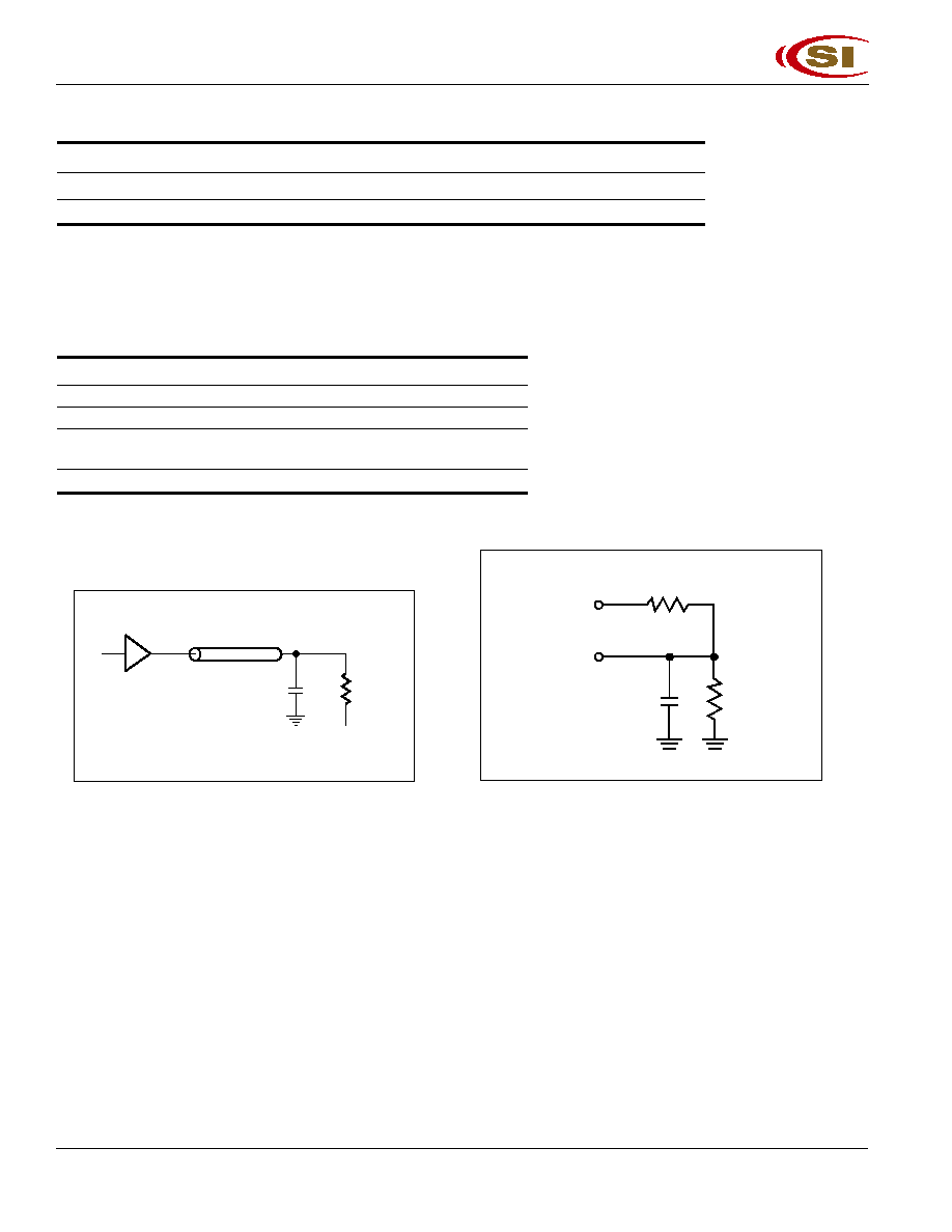
AC TEST LOADS
Figure 1
Output
Buffer
Z
O
= 50
1.5V
50
30 pF
Figure 2
317
5 pF
Including
jig and
scope
351
OUTPUT
3.3V

IS61NW6432
Integrated Circuit Solution Inc.
11
SSR006-0B
READ /WRITE CYCLE SWITCHING CHARACTERISTICS
(Over Operating Range)
-5
-6
-7
-8
Symbol Parameter
Min.
Max.
Min. Max. Min.
Max
Min.
Max.
Unit
fmax
Clock Frequency
100
83
75
66
MHz
t
KC
Cycle Time
10
12
13
15
ns
t
KH
Clock High Time
4
4
6
6
ns
t
KL
Clock Low Time
4
4
6
6
ns
t
KQ
Clock Access Time
5
6
7
8
ns
t
KQX
Clock High to Output Invalid
1.5
1.5
1.5
1.5
ns
t
KQLZ
Clock High to Output Low-Z
2.0
2.0
2.0
2.0
ns
t
KQHZ
Clock High to Output High-Z
1.5
3.5
2
3.5
2
3.5
2
3.5
ns
t
OEQ
Output Enable to Output Valid
5
6
6
6
ns
t
OEQX
Output Disable to Output Invalid
0
0
0
0
ns
t
OELZ
Output Enable to Output Low-Z
0
0
0
0
ns
t
OEHZ
Output Disable to Output High-Z
3.5
3.5
3.5
3.5
ns
t
AS
Address Setup Time
2.0
2.0
2.0
2.0
ns
t
WS
Read/Write Setup Time
2.0
2.0
2.0
2.0
ns
t
CES
Chip Enable Setup Time
2.0
2.0
2.0
2.0
ns
t
SE
Clock Enable Setup Time
2.0
2.0
2.0
2.0
ns
t
AVS
Address Advance Setup Time
2.0
2.0
2.0
2.0
ns
t
AE
Address Hold Time
0.5
0.5
0.5
0.5
ns
t
HE
Clock EnableHold Time
0.5
0.5
0.5
0.5
ns
t
WH
Write Hold Time
0.5
0.5
0.5
0.5
ns
t
CEH
Chip Enable Hold Time
0.5
0.5
0.5
0.5
ns
t
ALS
Advance/Load (ADV/LD) Setup Time2.0
2.0
2.0
2.0
ns
t
ALH
Advance/Load (ADV/LD) Hold Time 0.5
0.5
0.5
0.5
ns
tds
Data Setup Time
2.0
2.0
2.0
2.0
ns
tdh
Data Hold Time
0.5
0.5
0.5
0.5
ns
tzp
I/O From Tri-State to Valid
1.5
1.5
2.5
1.5
2.5
1.5
2.5
ns
Notes:
1. Configuration signal MODE is static and must not change during normal operation.
2. Guaranteed but not 100% tested. This parameter is periodically sampled.
IS61NW6432
12
Integrated Circuit Solution Inc.
SSR006-0B
READ/WRITE CYCLE TIMING
IS61NW6432
Integrated Circuit Solution Inc.
13
SSR006-0B
ORDERING INFORMATION
Commercial Range: 0∞C to +70∞C
Frequency (MHz)
Order Part Number
Package
5
IS61NW6432-5TQ 14*20*1.4mm LQFP
IS61NW6432-5PQ 14*20*2.7mm PQFP
6
IS61NW6432-6TQ 14*20*1.4mm LQFP
IS61NW6432-6PQ 14*20*2.7mm PQFP
7
IS61NW6432-7TQ 14*20*1.4mm LQFP
IS61NW6432-7PQ 14*20*2.7mm PQFP
8
IS61NW6432-8TQ 14*20*1.4mm LQFP
IS61NW6432-8PQ 14*20*2.7mm PQFP
Integrated Circuit Solution Inc.
HEADQUARTER:
NO.2, TECHNOLOGY RD. V, SCIENCE-BASED INDUSTRIAL PARK,
HSIN-CHU, TAIWAN, R.O.C.
TEL: 886-3-5780333
Fax: 886-3-5783000
BRANCH OFFICE:
7F, NO. 106, SEC. 1, HSIN-TAI 5
TH
ROAD,
HSICHIH TAIPEI COUNTY, TAIWAN, R.O.C.
TEL: 886-2-26962140
FAX: 886-2-26962252
http://www.icsi.com.tw

IS61NW6432
14
Integrated Circuit Solution Inc.
SSR006-0B