 | –≠–ª–µ–∫—Ç—Ä–æ–Ω–Ω—ã–π –∫–æ–º–ø–æ–Ω–µ–Ω—Ç: M650 | –°–∫–∞—á–∞—Ç—å:  PDF PDF  ZIP ZIP |

Integrated Circuit Systems, Inc. Communications Modules www.icst.com/Comm-Modules tel: 508-852-5400
M650 Series
Performance Specifications
1
Integrated Circuit Systems
The M650 Series of Voltage Controlled SAW
Oscillators is a low cost solution for many Telecom
applications. An internal SAW filter provides jitter
performance of less than 0.5psec (rms).
This device is specified for an operating
temperature range of -40∞C to +85∞C. A disable
feature forces the output into a static condition by
applying a logic "0" to the clock enable input. The
oscillator is housed in a hermetically-sealed,
leadless surface mount package.
The M650 Series of VCOs is available over an
output frequency range of 155MHz to 900MHz.
The device is most suited for phase-locked loop
applications as well as clock and data recovery
circuits.
Clock Smoothing for OC192/OC48/
OC12/OC3
Clock Smoothing for STS96/STS48/
STS12/STS3/STS1
Frequency Translation
Clock and Data Retiming
M650 Series
Voltage Controlled SAW Oscillators
Output Frequencies at 155MHz to
900MHz
Low Phase Jitter, 0.5psec (rms) typical
3.3 Volt Supply Operation
Complementary Outputs
Output Disable Feature
LCC Surface Mount Package
(9 x 14mm)
APPLICATION
FEATURES
DESCRIPTION
Operating Temp. Range (Case): ........................ -40∞C to +85∞C
Storage Temp. Range (Ambient): .................... -55∞C to +125∞C
Control Voltage Range: ................................................. 0 to V
CC
Output Current: ................................................................ 20 mA
Power Supply Voltage (Vcc): ................................ 0 to +3.6 Vdc
ABSOLUTE MAX RATINGS
9mm
14mm

M650 Series
Performance Specifications
Integrated Circuit Systems, Inc. Communications Modules www.icst.com/Comm-Modules tel: 508-852-5400
2
Integrated Circuit Systems
Specifications @ Vcc = +3.3 Volts, Vee = 0 Volts, and Ta = +25∞C unless otherwise specified
PARAMETER
Min
Typ
Max
Units
Output Frequency
155
900
MHz
Absolute Pull Range
±50
ppm
Frequency Stability (-40∞C to +85∞C)
-130
ppm
Duty Cycle
45
55
%
Spurious Suppression
-50
-60
dBc
Linearity
±6
%
Logic Levels
Vol
1
Vcc - 1.95
Vcc - 1.63
Volts
Voh
2
Vcc - 0.98
Vcc - 0.75
Volts
Input Control Voltage (Vc) Range
0
Vcc
Volts
VCO Gain
200
ppm/V
Vc Input Impedance
8
12
k
Vc Modulation BW
500
kHz
Clock/Output Enable (Pin 2)
2.0
Vcc +0.3
Volts
Clock/Output Disable (Pin 2)
-0.3
0.8
Volts
Output Rise Time
250
400
psec
Output Fall Time
250
400
psec
Jitter @ 155.520MHz offset from carrier
12kHz to 20MHz
0.230
psec rms
Jitter @ 622.080MHz offset from carrier
12kHz to 80MHz
0.458
psec rms
Phase Noise (offset from carrier)
100Hz
-65
dBc/Hz
1kHz
-95
dBc/Hz
10kHz
-120
dBc/Hz
100kHz
-140
dBc/Hz
Operating Temperature
-40
25
+85
∞C
Supply Current
Icc
80
95
mA
Supply Voltage
Vcc
3.2
3.3
3.4
V
Notes: 1. Output levels are standard 10K ECL and are fully 100K ECL compatible.
2. Transition times are measured from 20% to 80% of a full 10K ECL level swing.
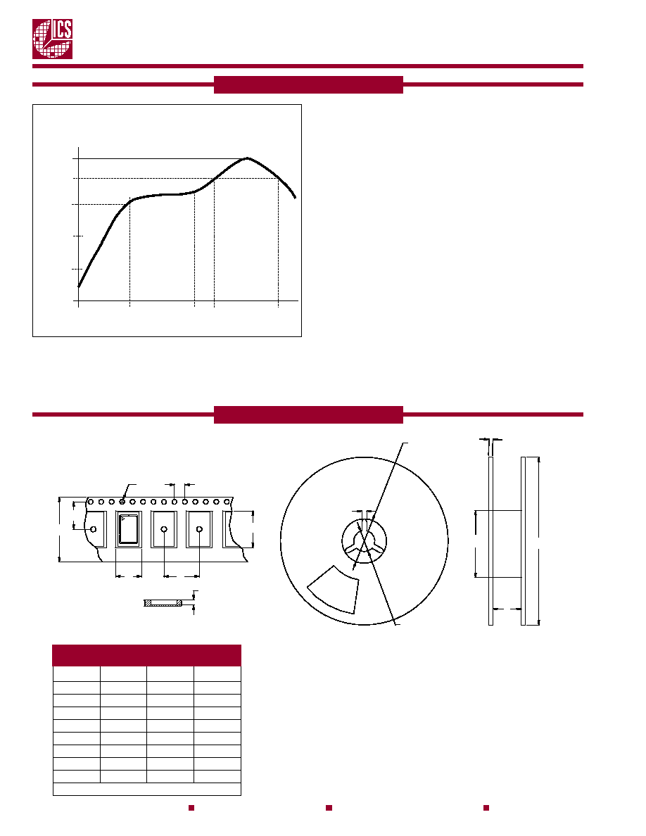
-170
-160
-150
-140
-130
-120
-110
-100
-90
1E+03
1E+04
1E+05
1E+0
Frequency in Hz
SSB Phase Noise dBc/Hz
SPECIFICATIONS
Phase Noise

Integrated Circuit Systems, Inc. Communications Modules www.icst.com/Comm-Modules tel: 508-852-5400
M650 Series
Performance Specifications
3
Integrated Circuit Systems
-15
-10
-5
0
5
10
3.15
3.2
3.25
3.3
3.35
3.4
3.45
Vcc (V)
PPM Deviation
Deviation (PPM)
Jitter
Output
622310000
622280000
622250000
622220000
622190000
622160000
622130000
622100000
622070000
622040000
622010000
621980000
0.2 0.4 0.6 08 1.0 1.2 1.4 1.6 1.8 2.0 2.2 2.4 2.6 2.8 3.0 3.2
Typical linearity of a M650 operating at 622.08 MHz
over the input range of .3 to 3.0 volts
Typical Linearity
SPECIFICATIONS
Typical Frequency Pushing
M650 Series
Performance Specifications
Integrated Circuit Systems, Inc. Communications Modules www.icst.com/Comm-Modules tel: 508-852-5400
4
Integrated Circuit Systems
Micro Networks has subjected their VCSO component
to various reflow profiles and test conditions for
optimum substrate mounting performance. The
conditions suggested here are recommended
temperature settings for the VCSO device during the
reflow processes. The best case condition for the
device is a slow ramp up to prevent thermal shock
before reaching reflow temperatures of Sn/Pb flux
activated solder with a melting point of 183 degree
Celsius. The M650 device should not see
temperatures above 183 degrees Celsius for an
extended periods beyond 60 seconds. Maximum
peak temperature for the device should not exceed
220 degrees Celsius for longer then 20 seconds.
Micro Networks has designed the M650 device as a
sealed unit. The package is 100% tested for seal
defects. Aqueous, solvent, or other wash type
cleaning methods is acceptable for this device.
IR REFLOW PROFILE
TAPE & REEL
A
B
C
D
E
F
G
H
I
N
O
J
K
L
M
180
220
150
100
50
60
60≠90
105≠150
Time (seconds)
T
emperature (
∞
C)
IR Reflow Profile
(Vendor Recommendation)
TAPE
MM
REEL
MM
A
24
F
1.78
B
11.5
G
21
C
1.5
H
13
D
4
I
100
E
12
J
5
M
9.2
K
25
N
14.5
L
330
O
3.7
No. per Reel: 300 Max
TAPE & REEL DIMENSIONS
Integrated Circuit Systems, Inc. Communications Modules www.icst.com/Comm-Modules tel: 508-852-5400
M650 Series
Performance Specifications
5
Integrated Circuit Systems
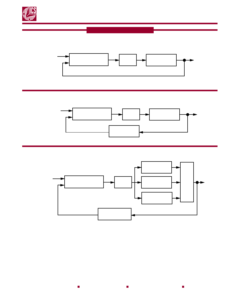
M650
155.520MHz
155.52MHz
155.52MHz
F and Frequency
Detector
Loop
Filter
APPLICATIONS
Jitter Attenuator
Frequency Translator
Multi-rate FEC Clock Generator
M650
666.5143MHz
M650
622.080MHz
M650
669.3266MHz
Programmable
Divider
Fin
Fout
F and Frequency
Detector
Loop
Filter
MUX
M650
622.080MHz
Divide by 32
19.44MHz
622.080MHz
F and Frequency
Detector
Loop
Filter
M650 Series
Performance Specifications
Integrated Circuit Systems, Inc. Communications Modules www.icst.com/Comm-Modules tel: 508-852-5400
6
Integrated Circuit Systems
MECHANICAL DIMENSIONS & PIN CONFIGURATION
Rev. 14.0
M650
Series
GND
Vcc
50 50
5
4
7
3
Output
Output
Control Voltage
Clock Enable
1
2
Vt
Vt = Vcc-2V
6
7
8
7
8
5
4
.550 [13.97]
1
2
3
3
2
1
4
5
ORIENTATION KEY
8X .040 [1.02]
8X .066 [1.68]
.200 [5.08]
.100 [2.54]
.350 [8.89]
.145 [3.28] MAX
Pin No.
Function
1
Control Voltage
2
Clock Enable
3
Case and Electrical Ground
4
GND
5
Output
6
Complimentary Output
7
Vcc
8
GND
ORDERING INFORMATION
BLOCK DIAGRAM
Part Number
M650P 622.0800
P for PECL Operation
Specify frequency in MHz xxx.xxxx
(eg. 155.5200MHz, 311.0400MHz,
622.0800MHz, 666.5140MHz)
Absolute Pull Range
Blank = ±50ppm
±100ppm available for certain frequencies.
Consult factory.
Integrated Circuit Systems, Inc.
Communications Modules
324 Clark Street
Worcester, MA 01606
tel: 508-852-5400
fax: 508-852-8456
European Sales Headquarters Hertogsingel 20 6214 AD Maastricht The Netherlands tel: +31-43-32-70912 fax: +31-43-32-70715
www.icst.com/Comm-Modules
ICS reserves the right to make changes in the device data identified in
this publication without further notice. ICS advises its customers to
obtain the latest version of all device data to verify that any information
being relied upon by the customer is current and accurate.