Integrated
Circuit
Systems, Inc.
8701-01
www.icst.com
REV. A - AUGUST 28, 2000
ICS8701-01
L
OW
S
KEW
¸1, ¸2 C
LOCK
G
ENERATOR
W
/P
OLARITY
C
ONTROL
1
G
ENERAL
D
ESCRIPTION
The ICS8701-01 is a low skew,
÷
1,
÷
2 Clock
Generator and a member of the HiPerClockS
family of High Performance Clock Solutions
from ICS. The low impedance LVCMOS outputs
are designed to drive 50
series or parallel ter-
minated transmission lines. The effective fanout can be in-
creased from 20 to 40 by utilizing the ability of the outputs to
drive two series terminated lines.
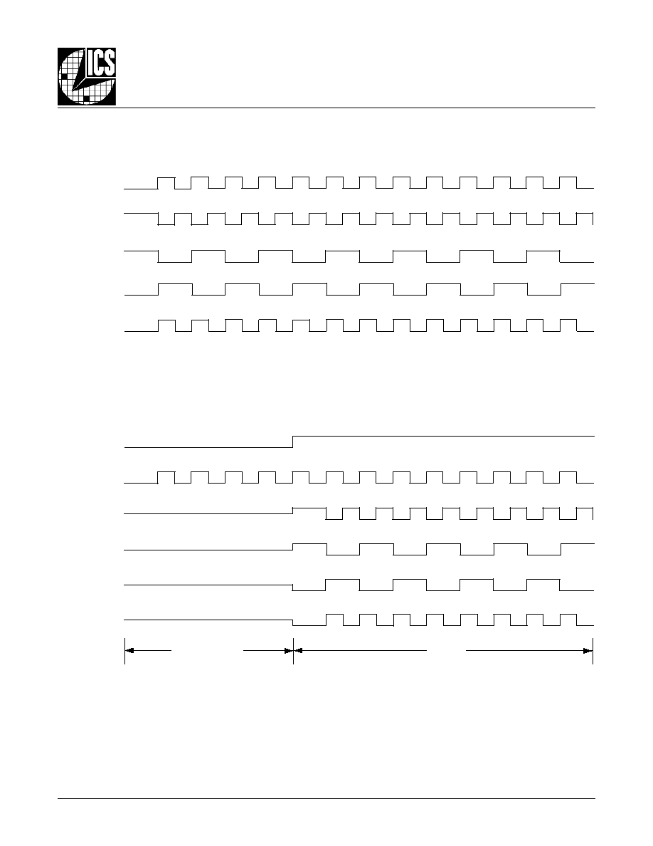
The divide select inputs, DIV_SELx, control the output fre-
quency of each bank. The outputs can be utilized in the ÷1,
÷2 or a combination of ÷1 and ÷2 modes. The master reset/
output enable input, nMR/OE, resets the internal dividers and
controls the active and high impedance states of all outputs.
The output polarity inputs, INV0:1, control the polarity (invert-
ing or non-inverting) of the outputs of each bank. Outputs
QA0-QA4 are inverting for every combination of the INV0:1
input. The timing relationship between the inverting and non-
inverting outputs at different frequencies is shown in the Tim-
ing Diagrams.
The ICS8701-01 is characterized at 3.3V and mixed 3.3V in-
put supply, and 2.5V output supply operating modes. Guar-
anteed bank, output and part-to-part skew characteristics
make the ICS8701-01 ideal for those clock distribution appli-
cations demanding well defined performance and repeatabil-
ity.
F
EATURES
20 LVCMOS outputs, 7
typical output impedance
Output frequency up to 250 MHz
250ps bank skew, 300ps output skew, 350ps multiple
frequency skew, 700ps part-to-part skew
Selectable inverting and non-inverting outputs
LVCMOS / LVTTL clock input
LVCMOS / LVTTL control inputs
Bank enable logic allows unused banks to be disabled
in reduced fanout applications
3.3V or mixed 3.3V input, 2.5V output operating
supply modes
48 lead low-profile QFP (LQFP), 7mm x 7mm x 1.4mm
package body, 0.5mm package lead pitch
0°C to 70°C ambient operating temperature
Other divide values available on request
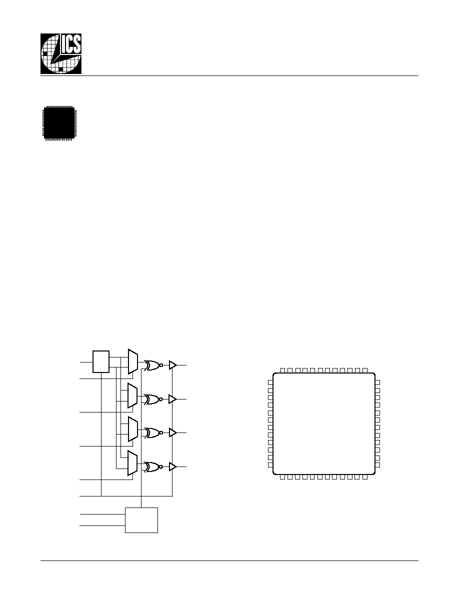
B
LOCK
D
IAGRAM
P
IN
A
SSIGNMENT
HiPerClockSTM
,&6
DIV_SELA
DIV_SELB
DIV_SELC
DIV_SELD
nMR/OE
INV0
INV1
QAO - QA4
QB0 - QB4
QC0 - QC4
QD0 - QD4
LVCMOS_CLK
1
0
÷1
÷2
1
0
1
0
1
0
Output
Polarity
Control
48 47 46 45 44 43 42 41 40 39 38 37
13 14 15 16 17 18 19 20 21 22 23 24
1
2
3
4
5
6
7
8
9
10
11
12
36
35
34
33
32
31
30
29
28
27
26
25
QC3
VDDOC
QC4
QD0
VDDOD
QD1
GND
QD2
GND
QD3
VDDOD
QD4
QB1
VDDOB
QB0
QA4
VDDOA
QA3
GND
QA2
GND
QA1
VDDOA
QA0
DIV_SELA
DIV_SELB
L
VCMOS_CLK
GND
VDDI
INV0
GND
INV1
VDDI
nMR/OE
DIV_SELC
DIV_SELD
GND
QB2
GND
QB3
VDDOB
QB4
QC0
VDDOC
QC1
GND
QC2
GND
48-Pin LQFP
Y Package
Top View
ICS8701-01