ICS8735AY-31
www.icst.com/products/hiperclocks.html
REV. A NOVEMBER 27, 2001
1
Integrated
Circuit
Systems, Inc.
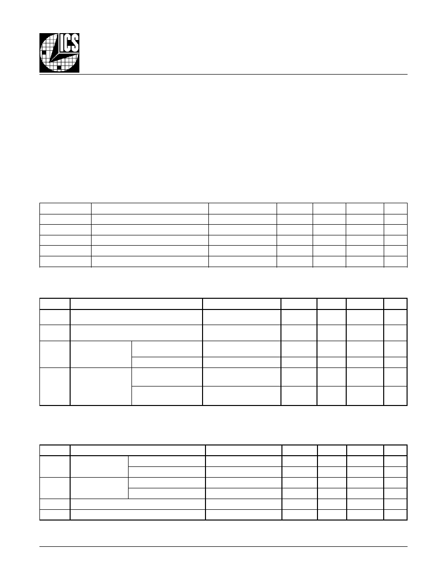
ICS8735-31
1:5 D
IFFERENTIAL
-
TO
-3.3V LVPECL
Z
ERO
D
ELAY
C
LOCK
G
ENERATOR
PRELIMINARY
G
ENERAL
D
ESCRIPTION
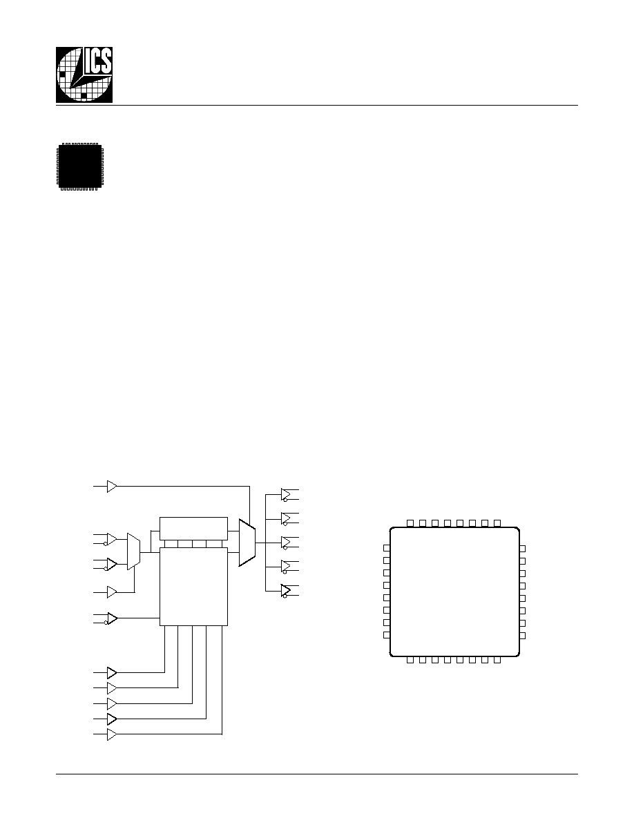
The ICS8735-31 is a highly versatile 1:5 Differ-
ential-to-3.3V LVPECL clock generator and a
member of the HiPerClockSTM family of High Per-
formance Clock Solutions from ICS. The
ICS8735-31 has a fully integrated PLL and can
be configured as zero delay buffer, multiplier or divider, and
has an output frequency range of 15.625MHz to 350MHz. The
reference divider, feedback divider and output divider are each
programmable, thereby allowing for the following output-to-
input frequency ratios: 8:1, 4:1, 2:1, 1:1, 1:2, 1:4, 1:8. The
external feedback allows the device to achieve "zero delay"
between the input clock and the output clocks. The PLL_SEL
pin can be used to bypass the PLL for system test and debug
purposes. In bypass mode, the reference clock is routed
around the PLL and into the internal output dividers.
F
EATURES
� 5 differential 3.3V LVPECL outputs
� Selectable differential clock inputs
� CLKx, nCLKx pair can accept the following differential input
levels: LVDS, LVPECL, LVHSTL, SSTL, HCSL
� Output frequency range: 15.625MHz - 350MHz
� Input frequency range: 15.625MHz - 350MHz
� VCO range: 250MHz - 700MHz
� Programmable dividers allow for the following output-to-input
frequency ratios: 8:1, 4:1, 2:1, 1:1, 1:2, 1:4, 1:8
� External feedback for "zero delay" clock regeneration
with configurable frequencies
� Cycle-to-cycle jitter: 30ps (typical)
� Output skew: 25ps (typical)
� Static phase offset: TBD � 100ps
� 3.3V supply voltage
� 0�C to 70�C ambient operating temperature
� Industrial temperature information available upon request
HiPerClockSTM
,&6
B
LOCK
D
IAGRAM
P
IN
A
SSIGNMENT
32-Lead QFP (LQFP)
7mm x 7mm x 1.4mm package body
Y Package
Top View
32 31 30 29 28 27 26 25
9 10 11 12 13 14 15 16
1
2
3
4
5
6
7
8
24
23
22
21
20
19
18
17
V
CCO
Q3
nQ3
Q2
nQ2
Q1
nQ1
V
CCO
SEL0
SEL1
CLK0
nCLK0
CLK1
nCLK1
CLK_SEL
MR
V
CCO
Q0
nQ0
V
EE
SEL2
FB_IN
nFB_IN
V
CC
V
CCO
nQ4
Q4
V
EE
SEL3
V
CCA
PLL_SEL
V
CC
ICS8735-31
The Preliminary Information presented herein represents a product in prototyping or pre-production. The noted characteristics are based on initial
product characterization. Integrated Circuit Systems, Incorporated (ICS) reserves the right to change any circuitry or specifications without notice.
PLL_SEL
CLK0
nCLK0
CLK1
nCLK1
CLK_SEL
FB_IN
nFB_IN
SEL0
SEL1
SEL2
SEL3
MR
Q0
nQ0
Q1
nQ1
Q2
nQ2
Q3
nQ3
Q4
nQ4
0
1
PLL
8:1, 4:1, 2:1, 1:1,
1:2, 1:4, 1:8
0
1
�2, �4, �8, �16,
�32
,
�64, �128
ICS8735AY-31
www.icst.com/products/hiperclocks.html
REV. A NOVEMBER 27, 2001
4
Integrated
Circuit
Systems, Inc.
ICS8735-31
1:5 D
IFFERENTIAL
-
TO
-3.3V LVPECL
Z
ERO
D
ELAY
C
LOCK
G
ENERATOR
PRELIMINARY
T
ABLE
4C. D
IFFERENTIAL
DC C
HARACTERISTICS
,
V
CC
= V
CCA
= V
CCO
= 3.3V�5%, T
A
= 0�C
TO
70�C
A
BSOLUTE
M
AXIMUM
R
ATINGS
Supply Voltage, V
CCx
4.6V
Inputs, V
I
-0.5V to V
CC
+0.5 V
Outputs, V
O
-0.5V to V
CCO
+0.5V
Package Thermal Impedance,
JA
47.9�C/W (0 lfpm)
Storage Temperature, T
STG
-65�C to 150�C
Stresses beyond those listed under Absolute Maximum Ratings may cause permanent damage to the device. These ratings are
stress specifications only. Functional operation of product at these conditions or any conditions beyond those listed in the
DC
Characteristics or AC Characteristics is not implied. Exposure to absolute maximum rating conditions for extended periods may
affect product reliability.
T
ABLE
4A. P
OWER
S
UPPLY
DC C
HARACTERISTICS
,
V
CC
= V
CCA
= V
CCO
= 3.3V�5%, T
A
= 0�C
TO
70�C
l
o
b
m
y
S
r
e
t
e
m
a
r
a
P
s
n
o
i
t
i
d
n
o
C
t
s
e
T
m
u
m
i
n
i
M
l
a
c
i
p
y
T
m
u
m
i
x
a
M
s
t
i
n
U
V
C
C
e
g
a
t
l
o
V
y
l
p
p
u
S
e
v
i
t
i
s
o
P
5
3
1
.
3
3
.
3
5
6
4
.
3
V
V
A
C
C
e
g
a
t
l
o
V
y
l
p
p
u
S
g
o
l
a
n
A
5
3
1
.
3
3
.
3
5
6
4
.
3
V
V
O
C
C
e
g
a
t
l
o
V
y
l
p
p
u
S
t
u
p
t
u
O
5
3
1
.
3
3
.
3
5
6
4
.
3
V
I
E
E
t
n
e
r
r
u
C
y
l
p
p
u
S
r
e
w
o
P
0
0
1
A
m
I
A
C
C
t
n
e
r
r
u
C
y
l
p
p
u
S
g
o
l
a
n
A
0
1
A
m
l
o
b
m
y
S
r
e
t
e
m
a
r
a
P
s
n
o
i
t
i
d
n
o
C
t
s
e
T
m
u
m
i
n
i
M
l
a
c
i
p
y
T
m
u
m
i
x
a
M
s
t
i
n
U
I
H
I
t
u
p
n
I
t
n
e
r
r
u
C
h
g
i
H
N
I
_
B
F
,
1
K
L
C
,
0
K
L
C
V
N
I
V
=
C
C
V
5
6
4
.
3
=
0
5
1
A
�
N
I
_
B
F
n
,
1
K
L
C
n
,
0
K
L
C
n
V
N
I
V
=
C
C
V
5
6
4
.
3
=
5
A
�
I
L
I
t
u
p
n
I
t
n
e
r
r
u
C
w
o
L
N
I
_
B
F
,
1
K
L
C
,
0
K
L
C
V
N
I
V
,
V
0
=
C
C
V
5
6
4
.
3
=
5
-
A
�
N
I
_
B
F
n
,
1
K
L
C
n
,
0
K
L
C
n
V
N
I
V
,
V
0
=
C
C
V
5
6
4
.
3
=
0
5
1
-
A
�
V
P
P
e
g
a
t
l
o
V
t
u
p
n
I
k
a
e
P
-
o
t
-
k
a
e
P
5
1
.
0
3
.
1
V
V
R
M
C
2
,
1
E
T
O
N
;
e
g
a
t
l
o
V
t
u
p
n
I
e
d
o
M
n
o
m
m
o
C
V
E
E
5
.
0
+
V
C
C
5
8
.
0
-
V
V
s
i
K
L
C
n
,
K
L
C
r
o
f
e
g
a
t
l
o
v
t
u
p
n
i
m
u
m
i
x
a
m
e
h
t
,
s
n
o
i
t
a
c
il
p
p
a
d
e
d
n
e
e
l
g
n
i
s
r
o
F
:
1
E
T
O
N
C
C
.
V
3
.
0
+
V
s
a
d
e
n
i
f
e
d
s
i
e
g
a
t
l
o
v
e
d
o
m
n
o
m
m
o
C
:
2
E
T
O
N
H
I
.
T
ABLE
4B. LVCMOS/LVTTL DC C
HARACTERISTICS
,
V
CC
= V
CCA
= V
CCO
= 3.3V�5%, T
A
= 0�C
TO
70�C
l
o
b
m
y
S
r
e
t
e
m
a
r
a
P
s
n
o
i
t
i
d
n
o
C
t
s
e
T
m
u
m
i
n
i
M
l
a
c
i
p
y
T
m
u
m
i
x
a
M
s
t
i
n
U
V
H
I
e
g
a
t
l
o
V
h
g
i
H
t
u
p
n
I
2
V
C
C
3
.
0
+
V
V
L
I
e
g
a
t
l
o
V
w
o
L
t
u
p
n
I
3
.
0
-
8
.
0
V
I
H
I
t
n
e
r
r
u
C
h
g
i
H
t
u
p
n
I
,
0
L
E
S
,
R
M
,
L
E
S
_
K
L
C
3
L
E
S
,
2
L
E
S
,
1
L
E
S
V
N
I
= *V
x
C
C
=
V
5
6
4
.
3
0
5
1
A
�
L
E
S
_
L
L
P
V
N
I
= *V
x
C
C
=
V
5
6
4
.
3
5
A
�
I
L
I
t
n
e
r
r
u
C
w
o
L
t
u
p
n
I
,
0
L
E
S
,
R
M
,
L
E
S
_
K
L
C
3
L
E
S
,
2
L
E
S
,
1
L
E
S
V
N
I
,
V
0
=
*V
x
C
C
V
5
6
4
.
3
=
5
-
A
�
L
E
S
_
L
L
P
V
N
I
,
V
0
=
*V
x
C
C
V
5
6
4
.
3
=
0
5
1
-
A
�
*
V
:
1
E
T
O
N
x
C
C
V
s
e
t
o
n
e
d
C
C
V
,
A
C
C
V
d
n
a
,
O
C
C
.