Äîêóìåíòàöèÿ è îïèñàíèÿ www.docs.chipfind.ru
ICS9248-136
Third party brands and names are the property of their respective owners.
Integrated
Circuit
Systems, Inc.
9248-136 Rev - 03/29/01
Advance Information
ADVANCE INFORMATION documents contain information on products
in the formative or design phase development. Characteristic data and
other specifications are design goals. ICS reserves the right to change or
discontinue these products without notice.
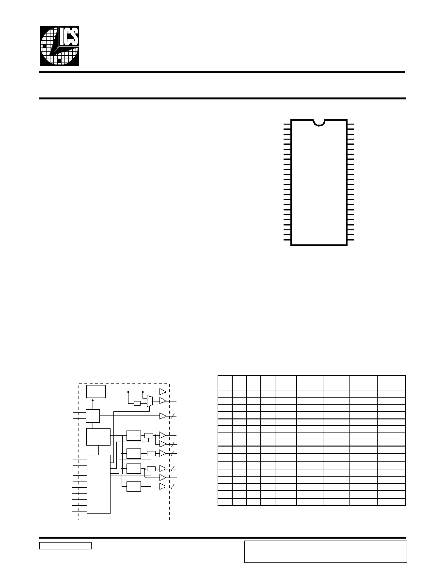
Frequency Generator & Integrated Buffers for K7 Processor
Block Diagram
Recommended Application:
Single chip clock solution for SIS 730S K7 chipset.
Output Features:
·
1 - Differential pair open drain CPU clock
·
1 - Single-ended open drain CPU clock
·
13 - SDRAM @ 3.3V
·
6- PCI @3.3V,
·
2 - AGP @ 3.3V
·
1- 48MHz, @3.3V fixed.
·
1- 24/48MHz, @3.3V selectable by I
2
C
(Default is 24MHz)
·
2- REF @3.3V, 14.318MHz.
Features:
·
Up to 166MHz frequency support
·
Support FS0-FS3 trapping status bit for I
2
C read back.
·
Support power management: CPU, PCI, SDRAM stop
and Power down Mode from I
2
C programming.
·
Spread spectrum for EMI control (0 to -0.5%, ± 0.25%).
·
Uses external 14.318MHz crystal
Skew Specifications:
·
CPU - CPU: < 175ps
·
SDRAM - SDRAM < 250ps
·
PCI - PCI: < 500ps
·
CPU - SDRAM: < 500ps
·
CPU (early) - PCI: 1-4ns (typ. 2ns)
Functionality
Pin Configuration
48-Pin 300mil SSOP
* These inputs have a 120K pull down to GND.
1 These are double strength.
VDDA
(AGPSEL)REF1
*(FS3)REF0
GND
X1
X2
VDDPCI
*(FS1)PCICLK_F
*(FS2)PCICLK0
PCICLK1
PCICLK2
PCICLK3
PCICLK4
GND
VDDAGP
AGPCLK0
AGPCLK1
GND
GND
*(FS0)48MHz
*(MODE)24_48MHz
VDD48
SDATA
SCLK
1
1
*
VDDCPU
CPUCLKT0
CPUCLKC0
CPUCLKT1
GND
VDDSDR
SDRAM0
SDRAM1
SDRAM2
GND
SDRAM3
SDRAM4
SDRAM5
VDDSDR
SDRAM6
SDRAM7
GND
SDRAM8/PD#
SDRAM9/SDRAM_STOP#
GND
SDRAM10/PCI_STOP#
SDRAM11/CPU_STOP#
SDRAM12
VDDSDR
ICS9248-136
1
2
3
4
5
6
7
8
9
10
11
12
13
14
15
16
17
18
19
20
21
22
23
24
48
47
46
45
44
43
42
41
40
39
38
37
36
35
34
33
32
31
30
29
28
27
26
25
PLL2
PLL1
Spread
Spectrum
48MHz
24_48MHz
CPUCLKC0
SDRAM (12:0)
PCICLK (4:0)
AGP (1:0)
CPUCLKT (1:0)
PCICLK_F
2
5
13
2
2
X1
X2
XTAL
OSC
CPU
DIVDER
SDRAM
DIVDER
PCI
DIVDER
Stop
Stop
Stop
SDATA
SCLK
FS (3:0)
PD#
PCI_STOP#
CPU_STOP#
SDRAM_STOP#
MODE
AGP_SEL
Control
Logic
Config.
Reg.
/ 2
REF (1:0)
AGP
DIVDER
0
0
0
0
100.00 100.00
33.33
66.67
50.00
0
0
0
1
100.00 133.33
33.33
66.67
50.00
0
0
1
0
100.00 150.00
30.00
60.00
50.00
0
0
1
1
100.00
66.67
33.33
66.67
50.00
0
1
0
0
112.00 112.00
33.60
67.20
56.00
0
1
0
1
125.00 100.00
31.25
62.50
50.00
0
1
1
0
124.00 124.00
31.00
62.00
46.50
0
1
1
1
133.33 100.00
33.33
66.67
50.00
1
0
0
0
133.33 133.33
33.33
66.67
50.00
1
0
0
1
150.00 150.00
30.00
60.00
50.00
1
0
1
0
111.11 166.67
33.33
66.67
55.56
1
0
1
1
110.00 165.00
33.00
66.00
55.00
1
1
0
0
166.67 166.67
33.33
66.67
55.56
1
1
0
1
90.00
90.00
30.00
60.00
45.00
1
1
1
0
48.00
48.00
32.00
64.00
48.00
1
1
1
1
45.00
60.00
30.00
60.00
45.00
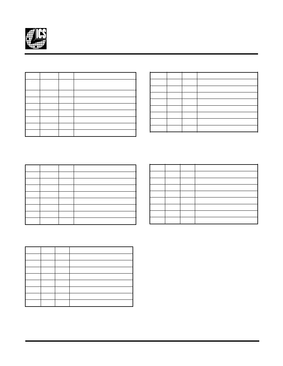
PCICLK
FS3 FS2 FS1 FS0 CPU
SDRAM
AGP
SEL = 0
AGP
SEL = 1
2
ICS9248-136
Advance Information
Third party brands and names are the property of their respective owners.
Pin Configuration
PIN NUMBER
PIN NAME
TYPE
DESCRIPTION
1, 7, 15, 22, 25,
35, 43, 48
VDD
PWR
3.3V Power supply for SDRAM output buffers, PCI output buffers,
reference output buffers and 48MHz output
AGPSEL
IN
AGP frequency select pin.
REF1
OUT
14.318 MHz reference clock.
FS3
IN
Frequency select pin.
REF0
OUT
14.318 MHz reference clock.
4, 14, 18, 19, 29,
32, 39, 44
GND
PWR
Ground pin for 3V outputs.
5
X1
IN
Crystal input,nominally 14.318M Hz.
6
X2
OUT
Crystal output, nominally 14.318MHz.
FS1
IN
Frequency select pin.
PCICLK_F
OUT
PCI clock output, not affected by PCI_STOP#
FS2
IN
Frequency select pin.
PCICLK0
OUT
PCI clock output.
13, 12, 11, 10
PCICLK (4:1)
OUT
PCI clock outputs.
17, 16
AGPCLK (1:0)
OUT
AGP outputs defined as 2X PCI. These may not be stopped.
FS0
IN
Frequency select pin.
48MHz
OUT
48M Hz output clock
M ODE
IN
Pin 27, 28, 30, & 31 function select pin
0=Desktop 1=M obile mode
24_48M Hz
OUT
Clock output for super I/O/USB default is 24M Hz
23
SDATA
I/O
Data pin for I
2
C circuitry 5V tolerant
24
SCLK
IN
Clock pin of I
2
C circuitry 5V tolerant
CPU_STOP#
IN
Stops all CPUCLKs clocks at logic 0 level, when input low
(when M ODE active).
SDRAM 11
OUT
SDRAM clock output
PCI_STOP#
IN
Stops all PCICLKs besides the PCICLK_F clocks at logic 0 level,
when input low (when M ODE active).
SDRAM 10
OUT
SDRAM clock output
SDRAM_STOP#
IN
Stops all SDRAM clocks at logic 0 level, when input low
(when M ODE active)
SDRAM9
OUT
SDRAM clock output
PD#
IN
Asynchronous active low input pin used to power down the device into a low
power state. The internal clocks are disabled and the VCO and the crystal are
stopped. The latency of the power down will not be greater than 3ms. (when
M ODE active)
SDRAM8
OUT
SDRAM clock output
26, 33, 34, 36, 37,
38, 40, 41, 42
SDRAM (12, 7:0)
OUT
SDRAM clock outputs
46
CPUCLKC0
OUT
Complementory"" clocks of differential pair CPU outputs. These clocks are
180° out of phase with SDRAM clocks. These open drain outputs need an
external 1.5V pull-up.
45, 47
CPUCLKT (1:0)
OUT
"True" clocks of differential pair CPU outputs. These clocks are in phase with
SDRAM clocks. These open drain outputs need an external 1.5V pull-up.
31
20
2
8
9
21
3
30
27
28
3
ICS9248-136
Advance Information
Third party brands and names are the property of their respective owners.
The ICS9248-136 is the single chip clock solution for Desktop/Notebook designs using the SIS 630S style chipset. It
provides all necessary clock signals for such a system.
Spread spectrum may be enabled through I
2
C programming. Spread spectrum typically reduces system EMI by 8dB to 10dB.
This simplifies EMI qualification without resorting to board design iterations or costly shielding. The ICS9248-136
employs a proprietary closed loop design, which tightly controls the percentage of spreading over process and temperature
variations.
Serial programming I
2
C interface allows changing functions, stop clock programming and frequency selection.
General Description
Power Groups
VDDCPU = CPU
VDDPCI = PCICLK_F, PCICLK
VDDSDR = SDRAM
VDD48 = 48MHz, 24MHz, fixed PLL
VDDA = Core, PLL, X1, X2
VDDAGP=AGP, REF
MODE Pin Power Management Control Input
E
D
O
M
1
2
n
i
P
7
2
n
i
P
8
2
n
i
P
0
3
n
i
P
1
3
n
i
P
0
1
1
M
A
R
D
S
0
1
M
A
R
D
S
9
M
A
R
D
S
8
M
A
R
D
S
1
#
P
O
T
S
_
U
P
C
#
P
O
T
S
_
I
C
P
#
P
O
T
S
_
M
A
R
D
S
#
D
P
4
ICS9248-136
Advance Information
Third party brands and names are the property of their respective owners.
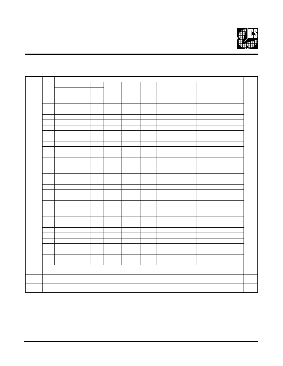
Byte0: Functionality and Frequency Select Register (default = 0)
Serial Configuration Command Bitmap
Note: PWD = Power-Up Default
Note1:
Default at power-up will be for latched logic inputs to define frequency, as displayed by Bit 3.
I
2
C is a trademark of Philips Corporation
ti
B
n
o
it
p
i
r
c
s
e
D
D
W
P
2
ti
B
4
:
7
ti
B
2
ti
B
7
ti
B
6
ti
B
5
ti
B
4
ti
B
U
P
C
M
A
R
D
S
I
C
P
P
G
A
0
=
L
E
S
P
G
A
1
=
L
E
S
e
g
a
t
n
e
c
e
r
P
d
a
e
r
p
S
0
0
0
0
0
1
e
t
o
N
3
S
F
2
S
F
1
S
F
0
S
F
0
0
0
0
0
0
0
.
0
0
1
0
0
.
0
0
1
3
3
.
3
3
7
6
.
6
6
0
0
.
0
5
d
a
e
r
p
S
n
w
o
D
%
5
.
0
-
o
t
0
0
0
0
0
1
0
0
.
0
0
1
3
3
.
3
3
1
3
3
.
3
3
7
6
.
6
6
0
0
.
0
5
d
a
e
r
p
S
n
w
o
D
%
5
.
0
-
o
t
0
0
0
0
1
0
0
0
.
0
0
1
0
0
.
0
5
1
0
0
.
0
3
0
0
.
0
6
0
0
.
0
5
d
a
e
r
p
S
r
e
t
n
e
C
%
5
2
.
0
-
/
+
0
0
0
1
1
0
0
.
0
0
1
7
6
.
6
6
3
3
.
3
3
7
6
.
6
6
0
0
.
0
5
d
a
e
r
p
S
n
w
o
D
%
5
.
0
-
o
t
0
0
0
1
0
0
0
0
.
2
1
1
0
0
.
2
1
1
0
6
.
3
3
0
2
.
7
6
0
0
.
6
5
d
a
e
r
p
S
r
e
t
n
e
C
%
5
2
.
0
-
/
+
0
0
1
0
1
0
0
.
5
2
1
0
0
.
0
0
1
5
2
.
1
3
0
5
.
2
6
0
0
.
0
5
d
a
e
r
p
S
r
e
t
n
e
C
%
5
2
.
0
-
/
+
0
0
1
1
0
0
0
.
4
2
1
0
0
.
4
2
1
0
0
.
1
3
0
0
.
2
6
0
5
.
6
4
d
a
e
r
p
S
r
e
t
n
e
C
%
5
2
.
0
-
/
+
0
0
1
1
1
3
3
.
3
3
1
0
0
.
0
0
1
3
3
.
3
3
7
6
.
6
6
0
0
.
0
5
d
a
e
r
p
S
n
w
o
D
%
5
.
0
-
o
t
0
0
1
0
0
0
3
3
.
3
3
1
3
3
.
3
3
1
3
3
.
3
3
7
6
.
6
6
0
0
.
0
5
d
a
e
r
p
S
n
w
o
D
%
5
.
0
-
o
t
0
0
1
0
0
1
0
0
.
0
5
1
0
0
.
0
5
1
0
0
.
0
3
0
0
.
0
6
0
0
.
0
5
d
a
e
r
p
S
r
e
t
n
e
C
%
5
2
.
0
-
/
+
0
1
0
1
0
1
1
.
1
1
1
7
6
.
6
6
1
3
3
.
3
3
7
6
.
6
6
6
5
.
5
5
d
a
e
r
p
S
r
e
t
n
e
C
%
5
2
.
0
-
/
+
0
1
0
1
1
0
0
.
0
1
1
0
0
.
5
6
1
0
0
.
3
3
0
0
.
6
6
0
0
.
5
5
d
a
e
r
p
S
r
e
t
n
e
C
%
5
2
.
0
-
/
+
0
1
1
0
0
7
6
.
6
6
1
7
6
.
6
6
1
3
3
.
3
3
7
6
.
6
6
6
5
.
5
5
d
a
e
r
p
S
r
e
t
n
e
C
%
5
2
.
0
-
/
+
0
1
1
0
1
0
0
.
0
9
0
0
.
0
9
0
0
.
0
3
0
0
.
0
6
0
0
.
5
4
d
a
e
r
p
S
r
e
t
n
e
C
%
5
2
.
0
-
/
+
0
1
1
1
0
0
0
.
8
4
0
0
.
8
4
0
0
.
2
3
0
0
.
4
6
0
0
.
8
4
d
a
e
r
p
S
r
e
t
n
e
C
%
5
2
.
0
-
/
+
0
1
1
1
1
0
0
.
5
4
0
0
.
0
6
0
0
.
0
3
0
0
.
0
6
0
0
.
5
4
d
a
e
r
p
S
r
e
t
n
e
C
%
5
2
.
0
-
/
+
1
0
0
0
0
0
3
.
0
0
1
0
3
.
0
0
1
3
4
.
3
3
7
8
.
6
6
5
1
.
0
5
d
a
e
r
p
S
r
e
t
n
e
C
%
5
2
.
0
-
/
+
1
0
0
0
1
0
3
.
0
0
1
3
7
.
3
3
1
3
4
.
3
3
7
8
.
6
6
5
1
.
0
5
d
a
e
r
p
S
r
e
t
n
e
C
%
5
2
.
0
-
/
+
1
0
0
1
0
0
0
.
5
0
1
0
5
.
7
5
1
0
5
.
1
3
0
0
.
3
6
0
5
.
2
5
d
a
e
r
p
S
r
e
t
n
e
C
%
5
2
.
0
-
/
+
1
0
0
1
1
0
3
.
0
0
1
7
8
.
6
6
3
4
.
3
3
7
8
.
6
6
5
1
.
0
5
d
a
e
r
p
S
r
e
t
n
e
C
%
5
2
.
0
-
/
+
1
0
1
0
0
0
0
.
0
1
1
0
0
.
0
1
1
0
0
.
3
3
0
0
.
6
6
0
0
.
5
5
d
a
e
r
p
S
r
e
t
n
e
C
%
5
2
.
0
-
/
+
1
0
1
0
1
0
0
.
3
0
1
0
0
.
3
0
1
3
3
.
4
3
7
6
.
8
6
0
5
.
1
5
d
a
e
r
p
S
r
e
t
n
e
C
%
5
2
.
0
-
/
+
1
0
1
1
0
0
0
.
3
0
1
3
3
.
7
3
1
3
3
.
4
3
7
6
.
8
6
0
5
.
1
5
d
a
e
r
p
S
r
e
t
n
e
C
%
5
2
.
0
-
/
+
1
0
1
1
1
3
7
.
3
3
1
0
3
.
0
0
1
3
4
.
3
3
7
8
.
6
6
5
1
.
0
5
d
a
e
r
p
S
r
e
t
n
e
C
%
5
2
.
0
-
/
+
1
1
0
0
0
3
7
.
3
3
1
3
7
.
3
3
1
3
4
.
3
3
7
8
.
6
6
5
1
.
0
5
d
a
e
r
p
S
r
e
t
n
e
C
%
5
2
.
0
-
/
+
1
1
0
0
1
0
0
.
0
4
1
0
0
.
0
4
1
0
0
.
5
3
0
0
.
0
7
0
5
.
2
5
d
a
e
r
p
S
r
e
t
n
e
C
%
5
2
.
0
-
/
+
1
1
0
1
0
3
3
.
7
3
1
0
0
.
3
0
1
3
3
.
4
3
7
6
.
8
6
0
5
.
1
5
d
a
e
r
p
S
r
e
t
n
e
C
%
5
2
.
0
-
/
+
1
1
0
1
1
3
3
.
7
3
1
3
3
.
7
3
1
3
3
.
4
3
7
6
.
8
6
0
5
.
1
5
d
a
e
r
p
S
r
e
t
n
e
C
%
5
2
.
0
-
/
+
1
1
1
0
0
0
0
.
5
0
1
0
0
.
5
0
1
0
0
.
5
3
0
0
.
0
7
0
5
.
2
5
d
a
e
r
p
S
r
e
t
n
e
C
%
5
2
.
0
-
/
+
1
1
1
0
1
3
3
.
8
3
1
3
3
.
8
3
1
8
5
.
4
3
7
1
.
9
6
8
8
.
1
5
d
a
e
r
p
S
r
e
t
n
e
C
%
5
2
.
0
-
/
+
1
1
1
1
0
0
0
.
0
0
2
0
0
.
0
0
2
3
3
.
3
3
7
6
.
6
6
0
0
.
0
5
d
a
e
r
p
S
r
e
t
n
e
C
%
5
2
.
0
-
/
+
1
1
1
1
1
5
2
.
4
0
1
0
0
.
9
3
1
5
7
.
4
3
0
5
.
9
6
3
1
.
2
5
d
a
e
r
p
S
r
e
t
n
e
C
%
5
2
.
0
-
/
+
3
ti
B
s
t
u
p
n
I
d
e
h
c
t
a
L
,t
c
e
l
e
s
e
r
a
w
d
r
a
h
y
b
d
e
t
c
e
l
e
s
s
i
y
c
n
e
u
q
e
r
F
-
0
4
:
7
2
,
ti
B
y
b
d
e
t
c
e
l
e
s
s
i
y
c
n
e
u
q
e
r
F
-
1
0
1
ti
B
l
a
m
r
o
N
-
0
d
e
l
b
a
n
E
m
u
r
t
c
e
p
S
d
a
e
r
p
S
-
1
0
0
ti
B
g
n
i
n
n
u
R
-
0
s
t
u
p
t
u
o
ll
a
e
t
a
t
s
i
r
T
-
1
0
5
ICS9248-136
Advance Information
Third party brands and names are the property of their respective owners.
Byte 1: CPU, Active/Inactive Register
(1= enable, 0 = disable)
Byte 2: PCI, Active/Inactive Register
(1= enable, 0 = disable)
T
I
B
#
N
I
P
D
W
P
N
O
I
T
P
I
R
C
S
E
D
7
t
i
B
-
1
d
e
v
r
e
s
e
R
6
t
i
B
-
1
d
e
v
r
e
s
e
R
5
t
i
B
3
1
1
4
K
L
C
I
C
P
4
t
i
B
2
1
1
3
K
L
C
I
C
P
3
t
i
B
1
1
1
2
K
L
C
I
C
P
2
t
i
B
0
1
1
1
K
L
C
I
C
P
1
t
i
B
9
1
0
K
L
C
I
C
P
0
t
i
B
8
1
F
_
K
L
C
I
C
P
Notes:
1. Inactive means outputs are held LOW and are disabled
from switching.
2. Latched Frequency Selects (FS#) will be inverted logic
load of the input frequency select pin conditions.
T
I
B
#
N
I
P
D
W
P
N
O
I
T
P
I
R
C
S
E
D
7
t
i
B
-
1
d
e
v
r
e
s
e
R
6
t
i
B
1
2
1
z
H
M
8
4
_
4
2
5
t
i
B
0
2
1
z
H
M
8
4
4
t
i
B
6
2
1
2
1
M
A
R
D
S
3
t
i
B
7
2
1
1
1
M
A
R
D
S
2
t
i
B
8
2
1
0
1
M
A
R
D
S
1
t
i
B
0
3
1
9
M
A
R
D
S
0
t
i
B
1
3
1
8
M
A
R
D
S
Byte 4: SDRAM , Active/Inactive Register
(1= enable, 0 = disable)
T
I
B
#
N
I
P
D
W
P
N
O
I
T
P
I
R
C
S
E
D
7
t
i
B
-
X
)
k
c
a
b
d
a
e
R
(
3
S
F
6
t
i
B
-
X
)
k
c
a
b
d
a
e
R
(
2
S
F
5
t
i
B
-
X
)
k
c
a
b
d
a
e
R
(
1
S
F
4
t
i
B
-
X
)
k
c
a
b
d
a
e
R
(
0
S
F
3
t
i
B
3
1
1
F
E
R
2
t
i
B
2
1
0
F
E
R
1
t
i
B
7
1
1
1
K
L
C
P
G
A
0
t
i
B
6
1
1
0
K
L
C
P
G
A
Byte 5: AGP, Active/Inactive Register
(1= enable, 0 = disable)
Byte 3: SDRAM, Active/Inactive Register
(1= enable, 0 = disable)
T
I
B
#
N
I
P
D
W
P
N
O
I
T
P
I
R
C
S
E
D
7
t
i
B
3
3
1
7
M
A
R
D
S
6
t
i
B
4
3
1
6
M
A
R
D
S
5
t
i
B
6
3
1
5
M
A
R
D
S
4
t
i
B
7
3
1
4
M
A
R
D
S
3
t
i
B
8
3
1
3
M
A
R
D
S
2
t
i
B
0
4
1
2
M
A
R
D
S
1
t
i
B
1
4
1
1
M
A
R
D
S
0
t
i
B
2
4
1
0
M
A
R
D
S
T
I
B
#
N
I
P
D
W
P
N
O
I
T
P
I
R
C
S
E
D
7
t
i
B
-
1
8
4
_
4
2
l
e
S
)
z
H
M
8
4
:
0
,
z
H
M
4
2
:
1
(
6
t
i
B
-
1
d
e
v
r
e
s
e
R
5
t
i
B
-
1
d
e
v
r
e
s
e
R
4
t
i
B
-
1
d
e
v
r
e
s
e
R
3
t
i
B
7
4
1
0
T
K
L
C
U
P
C
2
t
i
B
6
4
1
0
C
K
L
C
U
P
C
1
t
i
B
5
4
1
1
T
K
L
C
U
P
C
0
t
i
B
-
1
d
e
v
r
e
s
e
R