 | –≠–ª–µ–∫—Ç—Ä–æ–Ω–Ω—ã–π –∫–æ–º–ø–æ–Ω–µ–Ω—Ç: ICS950227 | –°–∫–∞—á–∞—Ç—å:  PDF PDF  ZIP ZIP |

Integrated
Circuit
Systems, Inc.
ICS950227
0641D--07/03/03
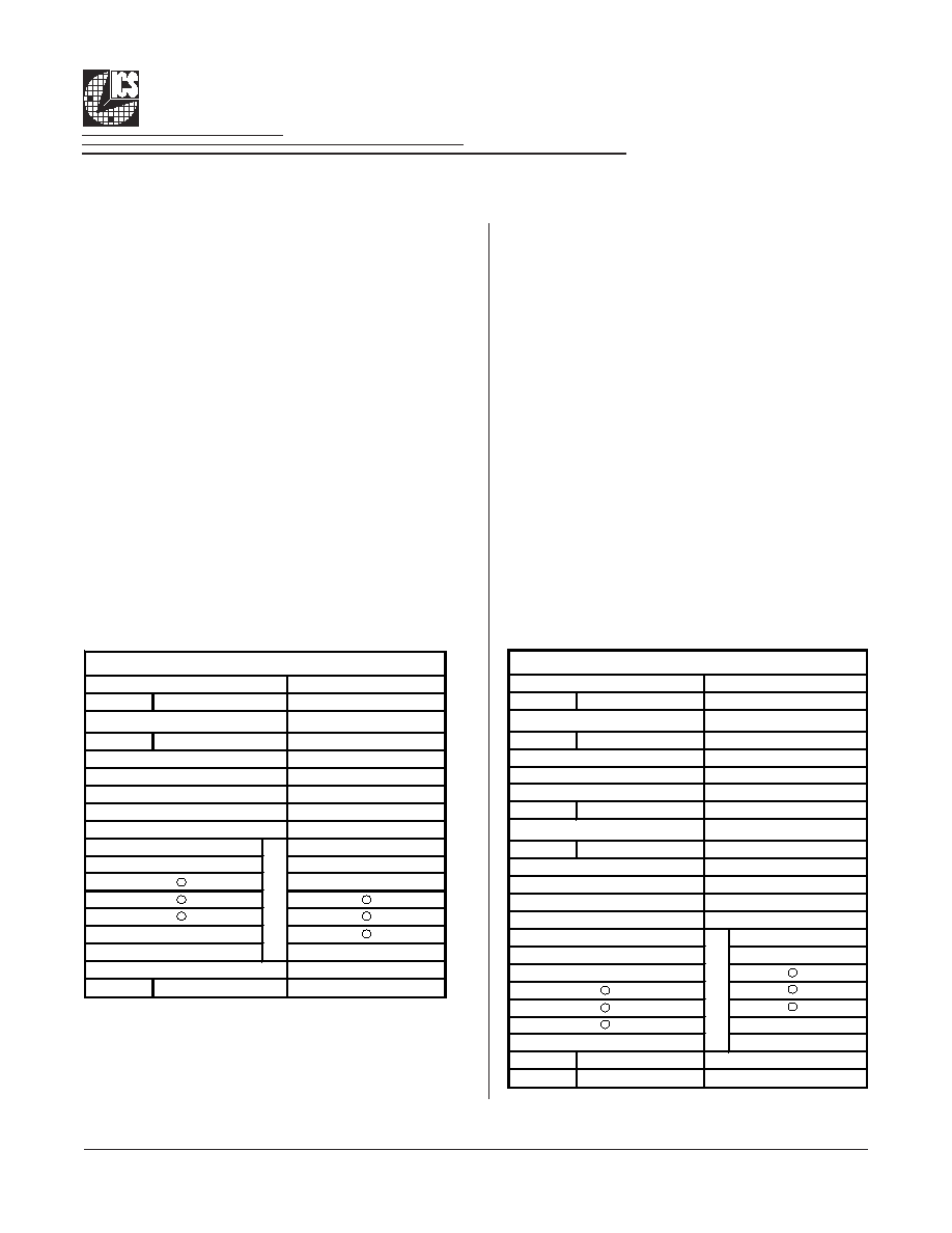
Block Diagram
Pin Configuration
56-Pin 300-mil SSOP
Frequency Table
Recommended Application:
CK-408 clock IntelÆ 845 with P4 processor.
Output Features:
∑
3 Differential CPU Clock Pairs @ 3.3V
∑
7 PCI (3.3V) @ 33.3MHz
∑
3 PCI_F (3.3V) @ 33.3MHz
∑
1 USB (3.3V) @ 48MHz
∑
1 DOT (3.3V) @ 48MHz
∑
1 REF (3.3V) @ 14.318MHz
∑
5 3V66 (3.3V) @ 66.6MHz
∑
1 VCH/3V66 (3.3V) @ 48MHz or 66.6MHz
Features/Benefits:
∑
Programmable output frequency.
∑
Programmable output divider ratios.
∑
Programmable output rise/fall time.
∑
Programmable output skew.
∑
Programmable spread percentage for EMI control.
∑
Watchdog timer technology to reset system
if system malfunctions.
∑
Programmable watch dog safe frequency.
∑
Support I
2
C Index read/write and block read/write
operations.
∑
Uses external 14.318MHz crystal.
Key Specifications:
∑
CPU Output Jitter <150ps
∑
3V66 Output Jitter <250ps
∑
CPU Output Skew <100ps
* These inputs have 150K internal pull-up resistor to VDD.
Programmable Timing Control HubTM for P4TM
2
S
F
1
S
F
0
S
F
U
P
C
)
z
H
M
(
6
6
V
3
)
z
H
M
(
]
0
:
2
[
f
f
u
B
6
6
]
2
:
4
[
6
6
V
3
)
z
H
M
(
F
_
I
C
P
I
C
P
)
z
H
M
(
0
0
0
6
6
.
6
6
6
6
.
6
6
6
6
.
6
6
3
3
.
3
3
0
0
1
0
0
.
0
0
1
6
6
.
6
6
6
6
.
6
6
3
3
.
3
3
0
1
0
0
0
.
0
0
2
6
6
.
6
6
6
6
.
6
6
3
3
.
3
3
0
1
1
3
3
.
3
3
1
6
6
.
6
6
6
6
.
6
6
3
3
.
3
3
d
i
M
0
0
e
t
a
t
s
i
r
T
e
t
a
t
s
i
r
T
e
t
a
t
s
i
r
T
e
t
a
t
s
i
r
T
d
i
M
0
1
2
/
K
L
C
T
4
/
K
L
C
T
4
/
K
L
C
T
8
/
K
L
C
T
d
i
M
1
0
d
e
v
r
e
s
e
R
d
e
v
r
e
s
e
R
d
e
v
r
e
s
e
R
d
e
v
r
e
s
e
R
d
i
M
1
1
d
e
v
r
e
s
e
R
d
e
v
r
e
s
e
R
d
e
v
r
e
s
e
R
d
e
v
r
e
s
e
R
VDDREF
1
56 REF
X1
2
55 FS1
X2
3
54 FS0
GND
4
53 CPU_STOP#*
PCICLK_F0
5
52 CPUCLKT0
PCICLK_F1
6
51 CPUCLKC0
PCICLK_F2
7
50 VDDCPU
VDDPCI
8
49 CPUCLKT1
GND
9
48 CPUCLKC1
PCICLK0 10
47 GND
PCICLK1 11
46 VDDCPU
PCICLK2 12
45 CPUCLKT2
PCICLK3 13
44 CPUCLKC2
VDDPCI 14
43 MULTSEL0*
GND 15
42 IREF
PCICLK4 16
41 GND
PCICLK5 17
40 FS2
PCICLK6 18
39 48MHz_USB
VDD3V66 19
38 48MHz_DOT
GND 20
37 VDD48
3V66_2 21
36 GND
3V66_3 22
35 3V66_1/VCH_CLK
3V66_4 23
34 PCI_STOP#*
3V66_5 24
33 3V66_0
*PD# 25
32 VDD3V66
VDDA 26
31 GND
GND 27
30 SCLK
Vtt_PWRGD# 28
29 SDATA
I
C
S
950227
PLL2
PLL1
Spread
Spectrum
48MHz_USB
PCICLK (6:0)
3V66 (5:2,0)
48MHz_DOT
3V66_1/VCH_CLK
X1
WDEN
XTAL
OSC
CPU
DIVDER
PCI
DIVDER
3V66
DIVDER
PD#
CPU_STOP#
PCI_STOP#
MULTSEL0
SDATA
SCLK
Vtt_PWRGD#
FS (2:0)
I REF
Control
Logic
Config.
Reg.
REF
3
3
7
5
3
CPUCLKT (2:0)
CPUCLKC (2:0)
PCICLK_F (2:0)
Stop
Stop

2
Integrated
Circuit
Systems, Inc.
ICS950227
0641D--07/03/03
Pin Description
Power Groups
(Analog)
(Digital)
VDDA = Analog Core PLL1
VDDPCI
VDDREF = REF, Xtal
VDD3V66
VDD48 = 48MHz, PLL
VDDCPU
R
E
B
M
U
N
N
I
P
E
M
A
N
N
I
P
E
P
Y
T
N
O
I
T
P
I
R
C
S
E
D
,
6
2
,
9
1
,
4
1
,
8
,
1
0
5
,
6
4
,
7
3
,
2
3
D
D
V
R
W
P
y
l
p
p
u
s
r
e
w
o
p
V
3
.
3
2
1
X
l
a
t
s
y
r
C
2
X
t
u
p
n
I
t
u
p
n
i
l
a
t
s
y
r
C
z
H
M
8
1
3
.
4
1
3
2
X
l
a
t
s
y
r
C
1
X
t
u
p
t
u
O
t
u
p
t
u
o
l
a
t
s
y
r
C
z
H
M
8
1
3
.
4
1
5
,
6
,
7
)
0
:
2
(
F
_
K
L
C
I
C
P
T
U
O
#
P
O
T
S
_
I
C
P
y
b
d
e
t
c
e
f
f
a
t
o
n
k
c
o
l
c
I
C
P
g
n
i
n
n
u
r
e
e
r
F
.
t
n
e
m
e
g
a
n
a
m
r
e
w
o
p
r
o
f
,
7
2
,
0
2
,
5
1
,
9
,
4
7
4
,
1
4
,
6
3
,
1
3
D
N
G
R
W
P
y
l
p
p
u
s
V
3
.
3
r
o
f
s
n
i
p
d
n
u
o
r
G
,
3
1
,
6
1
,
7
1
,
8
1
0
1
,
1
1
,
2
1
)
0
:
6
(
K
L
C
I
C
P
T
U
O
s
t
u
p
t
u
o
k
c
o
l
c
I
C
P
1
2
,
2
2
,
3
2
,
4
2
)
2
:
5
(
6
6
V
3
T
U
O
O
C
V
l
a
n
r
e
t
n
i
m
o
r
f
,
s
k
c
o
l
c
e
c
n
e
r
e
f
e
r
z
H
M
6
6
5
2
#
D
P
N
I
.
w
o
L
e
v
i
t
c
A
.
e
d
o
m
n
w
o
d
-
r
e
w
o
p
s
e
k
o
v
n
I
8
2
#
D
G
R
W
P
_
t
t
V
N
I
o
t
d
e
s
u
e
b
o
r
t
s
e
v
i
t
i
s
n
e
s
l
e
v
e
l
a
s
i
t
u
p
n
i
L
T
T
V
L
V
3
.
3
s
i
h
T
d
il
a
v
e
r
a
s
t
u
p
n
i
0
L
E
S
I
T
L
U
M
d
n
a
)
0
:
2
(
S
F
n
e
h
w
e
n
i
m
r
e
t
e
d
d
e
l
p
m
a
s
e
b
o
t
y
d
a
e
r
e
r
a
d
n
a
)
w
o
l
e
v
i
t
c
a
(
9
2
A
T
A
D
S
O
/
I
I
r
o
f
n
i
p
a
t
a
D
2
t
n
a
r
e
l
o
t
V
5
y
r
t
i
u
c
r
i
c
C
0
3
K
L
C
S
N
I
I
f
o
n
i
p
k
c
o
l
C
2
t
n
a
r
e
l
o
t
V
5
y
r
t
i
u
c
r
i
c
C
3
3
0
_
6
6
V
3
T
U
O
O
C
V
l
a
n
r
e
t
n
i
m
o
r
f
,
s
k
c
o
l
c
e
c
n
e
r
e
f
e
r
z
H
M
6
6
4
3
#
P
O
T
S
_
I
C
P
N
I
t
p
e
c
x
e
w
o
l
t
u
p
n
i
n
e
h
w
,
l
e
v
e
l
0
c
i
g
o
l
t
a
s
k
c
o
l
c
K
L
C
I
C
P
s
t
l
a
H
g
n
i
n
n
u
r
e
e
r
f
e
r
a
h
c
i
h
w
F
_
K
L
C
I
C
P
5
3
K
L
C
_
H
C
V
/
1
_
6
6
V
3
T
U
O
h
g
u
o
r
h
t
e
l
b
a
t
c
e
l
e
s
t
u
p
t
u
o
V
3
.
3
I
2
C
O
C
V
l
a
n
r
e
t
n
i
m
o
r
f
z
H
M
6
6
e
b
o
t
r
o
)
C
S
S
-
n
o
n
(
z
H
M
8
4
8
3
T
O
D
_
z
H
M
8
4
T
U
O
T
O
D
r
o
f
k
c
o
l
c
t
u
p
t
u
o
z
H
M
8
4
9
3
B
S
U
_
z
H
M
8
4
T
U
O
B
S
U
r
o
f
k
c
o
l
c
t
u
p
t
u
o
z
H
M
8
4
0
4
2
S
F
N
I
1
c
i
g
o
l
e
b
t
o
n
n
a
c
,
n
o
i
t
c
e
l
e
s
e
d
o
M
r
o
f
t
u
p
n
i
V
3
.
3
l
a
i
c
e
p
S
2
4
F
E
R
I
T
U
O
.
s
r
i
a
p
K
L
C
U
P
C
e
h
t
r
o
f
t
n
e
r
r
u
c
e
c
n
e
r
e
f
e
r
e
h
t
s
e
h
s
il
b
a
t
s
e
n
i
p
s
i
h
T
o
t
r
e
d
r
o
n
i
d
n
u
o
r
g
o
t
d
e
i
t
r
o
t
s
i
s
e
r
n
o
i
s
i
c
e
r
p
d
e
x
i
f
a
s
e
r
i
u
q
e
r
n
i
p
s
i
h
T
.
t
n
e
r
r
u
c
e
t
a
i
r
p
o
r
p
p
a
e
h
t
h
s
il
b
a
t
s
e
3
4
0
L
E
S
T
L
U
M
N
I
s
t
u
p
t
u
o
U
P
C
r
o
f
r
e
il
p
i
t
l
u
m
t
n
e
r
r
u
c
e
h
t
g
n
i
t
c
e
l
e
s
r
o
f
t
u
p
n
i
L
T
T
V
L
V
3
.
3
1
5
,
8
4
,
4
4
)
0
:
2
(
C
K
L
C
U
P
C
T
U
O
e
r
a
e
s
e
h
T
.
s
t
u
p
t
u
o
U
P
C
r
i
a
p
l
a
i
t
n
e
r
e
f
f
i
d
f
o
s
k
c
o
l
c
"
y
r
o
t
n
e
m
e
l
p
m
o
C
"
.
s
a
i
b
e
g
a
t
l
o
v
r
o
f
d
e
r
i
u
q
e
r
e
r
a
s
r
o
t
s
i
s
e
r
l
a
n
r
e
t
x
e
d
n
a
s
t
u
p
t
u
o
t
n
e
r
r
u
c
2
5
,
9
4
,
5
4
)
0
:
2
(
T
K
L
C
U
P
C
T
U
O
t
n
e
r
r
u
c
e
r
a
e
s
e
h
T
.
s
t
u
p
t
u
o
U
P
C
r
i
a
p
l
a
i
t
n
e
r
e
f
f
i
d
f
o
s
k
c
o
l
c
"
e
u
r
T
"
.
s
a
i
b
e
g
a
t
l
o
v
r
o
f
d
e
r
i
u
q
e
r
e
r
a
s
r
o
t
s
i
s
e
r
l
a
n
r
e
t
x
e
d
n
a
s
t
u
p
t
u
o
3
5
#
P
O
T
S
_
U
P
C
N
I
w
o
l
t
u
p
n
i
n
e
h
w
,
l
e
v
e
l
0
c
i
g
o
l
t
a
s
k
c
o
l
c
K
L
C
U
P
C
s
t
l
a
H
4
5
,
5
5
)
0
:
1
(
S
F
N
I
s
n
i
p
t
c
e
l
e
s
y
c
n
e
u
q
e
r
F
6
5
F
E
R
T
U
O
.
k
c
o
l
c
e
c
n
e
r
e
f
e
r
z
H
M
8
1
3
.
4
1

3
Integrated
Circuit
Systems, Inc.
ICS950227
0641D--07/03/03
Host Swing Select Functions
Maximum Allowed Current
Truth Table
n
o
i
t
i
d
n
o
C
n
o
i
t
p
m
u
s
n
o
c
y
l
p
p
u
s
V
3
.
3
x
a
M
,
s
d
a
o
l
p
a
c
e
t
e
r
c
s
i
d
x
a
M
V
5
6
4
.
3
=
d
d
V
D
N
G
r
o
d
d
V
=
s
t
u
p
n
i
c
i
t
a
t
s
ll
A
e
d
o
M
n
w
o
d
r
e
w
o
P
)
0
=
#
N
W
D
R
W
P
(
A
m
0
4
e
v
i
t
c
A
l
l
u
F
A
m
0
6
3
2
S
F
1
S
F
0
S
F
U
P
C
)
z
H
M
(
)
0
:
5
(
6
6
V
3
)
z
H
M
(
F
_
I
C
P
I
C
P
)
z
H
M
(
0
F
E
R
)
z
H
M
(
T
O
D
/
B
S
U
)
z
H
M
(
0
0
0
6
6
.
6
6
6
6
.
6
6
3
3
.
3
3
8
1
3
.
4
1
0
0
.
8
4
0
0
1
0
0
.
0
0
1
6
6
.
6
6
3
3
.
3
3
8
1
3
.
4
1
0
0
.
8
4
0
1
0
0
0
.
0
0
2
6
6
.
6
6
3
3
.
3
3
8
1
3
.
4
1
0
0
.
8
4
0
1
1
3
3
.
3
3
1
6
6
.
6
6
3
3
.
3
3
8
1
3
.
4
1
0
0
.
8
4
d
i
M
0
0
e
t
a
t
s
i
r
T
e
t
a
t
s
i
r
T
e
t
a
t
s
i
r
T
e
t
a
t
s
i
r
T
e
t
a
t
s
i
r
T
d
i
M
0
1
2
/
K
L
C
T
4
/
K
L
C
T
8
/
K
L
C
T
K
L
C
T
2
/
K
L
C
T
d
i
M
1
0
d
e
v
r
e
s
e
R
d
e
v
r
e
s
e
R
d
e
v
r
e
s
e
R
d
e
v
r
e
s
e
R
d
e
v
r
e
s
e
R
d
i
M
1
1
d
e
v
r
e
s
e
R
d
e
v
r
e
s
e
R
d
e
v
r
e
s
e
R
d
e
v
r
e
s
e
R
d
e
v
r
e
s
e
R
0
L
E
S
I
T
L
U
M
t
e
g
r
a
T
d
r
a
o
B
Z
m
r
e
T
/
e
c
a
r
T
,
R
e
c
n
e
r
e
f
e
R
=
f
e
r
I
V
D
D
)
r
R
*
3
(
/
t
u
p
t
u
O
t
n
e
r
r
u
C
Z
@
h
o
V
1
s
m
h
o
0
5
,
%
1
5
7
4
=
r
R
A
m
2
3
.
2
=
f
e
r
I
F
E
R
I
*
6
=
h
o
I
0
5
@
V
7
.
0
4
Integrated
Circuit
Systems, Inc.
ICS950227
0641D--07/03/03
General I
2
C serial interface information
How to Write:
∑
Controller (host) sends a start bit.
∑ Controller (host) sends the write address D2
(H)
∑ ICS clock will
acknowledge
∑ Controller (host) sends the begining byte location = N
∑ ICS clock will
acknowledge
∑ Controller (host) sends the data byte count = X
∑ ICS clock will
acknowledge
∑ Controller (host) starts sending
Byte N through
Byte N + X -1
(see Note 2)
∑ ICS clock will
acknowledge each byte one at a time
∑ Controller (host) sends a Stop bit
How to Read:
∑ Controller (host) will send start bit.
∑ Controller (host) sends the write address D2
(H)
∑ ICS clock will
acknowledge
∑ Controller (host) sends the begining byte
location = N
∑ ICS clock will
acknowledge
∑ Controller (host) will send a separate start bit.
∑ Controller (host) sends the read address D3
(H)
∑ ICS clock will
acknowledge
∑ ICS clock will send the data byte count = X
∑ ICS clock sends
Byte N + X -1
∑ ICS clock sends
Byte 0 through byte X (if X
(H)
was written to byte 8)
.
∑ Controller (host) will need to acknowledge each
byte
∑ Controllor (host) will send a not acknowledge bit
∑ Controller (host) will send a stop bit
ICS (Slave/Receiver)
T
WR
ACK
ACK
ACK
ACK
ACK
P
stoP bit
X Byt
e
Index Block Write Operation
Slave Address D2
(H)
Beginning Byte = N
WRite
starT bit
Controller (Host)
Byte N + X - 1
Data Byte Count = X
Beginning Byte N
T
starT bit
WR
WRite
RT
Repeat starT
RD
ReaD
Beginning Byte N
Byte N + X - 1
N
Not acknowledge
P
stoP bit
Slave Address D3
(H)
Index Block Read Operation
Slave Address D2
(H)
Beginning Byte = N
ACK
ACK
Data Byte Count = X
ACK
ICS (Slave/Receiver)
Controller (Host)
X Byt
e
ACK
ACK

5
Integrated
Circuit
Systems, Inc.
ICS950227
0641D--07/03/03
I
2
C Table: Frequency Select Register
Pin #
Name
Control Function
Type
0
1
PWD
Bit 7
SPREAD ENABLE
Frequency H/W IIC
Select
RW
OFF
ON
0
Bit 6
CENTER/DOWNSP
READ SELECT
CENTER/DOWNSPRE
AD SELECT
RW
DOWN
SPREAD
CENTER
SPREAD
0
Bit 5
3V66/VCH SELECT 48MHz/66.66MHz SEL
RW
66.66MHz
48.00MHz
0
Bit 4
CPU_STOP#
CPU STOP Read Back
R
X
Bit 3
PCI_STOP#
HW/SW SELECT
Freq Select Bit 3
RW/R
PCI STOP
PCI
RUNNING
1
Bit 2
FS2
Freq Select 2 Read
Back
R
X
Bit 1
FS1
Freq Select 1 Read
Back
R
X
Bit 0
FS0
Freq Select 0 Read
Back
R
X
I
2
C Table: Spreading and Device Behavior Control Register
Pin #
Name
Control Function
Type
0
1
PWD
Bit 7
MULTSEL0
MULTSEL0
READBACK
R
X
Bit 6
WD ALARM
Watchdog Alarm Read
Back
R
NO ALARM
ALARM SET
0
Bit 5
CPU2/CPUC2
RW
STOPPABLE FREE-RUN
0
Bit 4
CPU1/CPUC1
RW
STOPPABLE FREE-RUN
0
Bit 3
CPU0/CPUC0
RW
STOPPABLE FREE-RUN
0
Bit 2
CPU2/CPUC2
Output Control
RW
Disable
Enable
1
Bit 1
CPU1/CPUC1
Output Control
RW
Disable
Enable
1
Bit 0
CPU0/CPUC0
Output Control
RW
Disable
Enable
1
I
2
C Table: Output Control Register
Pin #
Name
Control Function
Type
0
1
PWD
Bit 7
Reserved
Reserved
RW
-
-
0
Bit 6
PCICLK6
Output Control
RW
Disable
Enable
1
Bit 5
PCICLK5
Output Control
RW
Disable
Enable
1
Bit 4
PCICLK4
Output Control
RW
Disable
Enable
1
Bit 3
PCICLK3
Output Control
RW
Disable
Enable
1
Bit 2
PCICLK2
Output Control
RW
Disable
Enable
1
Bit 1
PCICLK1
Output Control
RW
Disable
Enable
1
Bit 0
PCICLK0
Output Control
RW
Disable
Enable
1
I
2
C Table: Output Control Register
Pin #
Name
Control Function
Type
0
1
PWD
Bit 7
48MHz_DOT
Output Control
RW
Disable
Enable
1
Bit 6
48MHz_USB
Output Control
RW
Disable
Enable
1
Bit 5
PCIF2
RW
FREE-RUN STOPPABLE
0
Bit 4
PCIF1
RW
FREE-RUN STOPPABLE
0
Bit 3
PCIF0
RW
FREE-RUN STOPPABLE
0
Bit 2
PCICLK_F2
Output Control
RW
Disable
Enable
1
Bit 1
PCICLK_F1
Output Control
RW
Disable
Enable
1
Bit 0
PCICLK_F0
Output Control
RW
Disable
Enable
1
5
7
6
5
READBACK
Byte 1
43
READBACK
53
34
40
55
54
READBACK
Byte 0
-
-
35
-
45, 44
49, 48
52, 51
17
16
13
Byte 2
-
18
45, 44
49, 48
52, 51
12
11
10
6
Byte 3
38
39
7
CPU FREE-RUN NING
CONTROL
CPU FREE-RUN NING
CONTROL