
M902-01 Datasheet Rev 2.1
Revised 24Jun2004
I n t e g r a t e d C i r c u i t S y s t e m s , I n c .
N e t w o r k i n g & C o m m u n i c a t i o n s
w w w. i c s t . c o m
t e l ( 5 0 8 ) 8 5 2 - 5 4 0 0
M902-01
VCSO B
ASED
G
B
E C
LOCK
G
ENERATOR
Integrated
Circuit
Systems, Inc.
P r o d u c t D a t a S h e e t
G
ENERAL
D
ESCRIPTION
The M902-01 is a PLL (Phase Locked Loop) based
clock generator that uses an
internal VCSO (Voltage Controlled
SAW Oscillator) to produce a very
low jitter output clock. It is ideal for
Gigabit Ethernet. The output clock
(frequency of
156.25
or
187.50
MHz
for example) is provided from two
LVPECL clock output pairs. (Specify frequency at time
of order.) The accuracy of the output frequency is
assured by the internal PLL, which phase-locks the
internal VCSO to the reference input frequency (
25
or
30
MHz for example). The input reference can either
be an external crystal, utilizing the internal crystal
oscillator, or a stable external clock source such as
a packaged crystal oscillator.
F
EATURES
Output clock frequency from 125MHz to 190MHz
(Consult factory for frequency availability)
Two identical LVPECL output pairs
Integrated SAW (surface acoustic wave) delay line
Low jitter 0.5ps rms (over 12kHz-20MHz)
Ideal for Gigabit Ethernet
clock reference
Output-to-output skew < 100ps
External XTAL or LVCMOS reference input
Selectable external feed-through clock input
STOP clock control (Logic 1 stops output clocks)
Industrial temperature grade available
Single 3.3V power supply
Small 9 x 9 mm SMT (surface mount) package
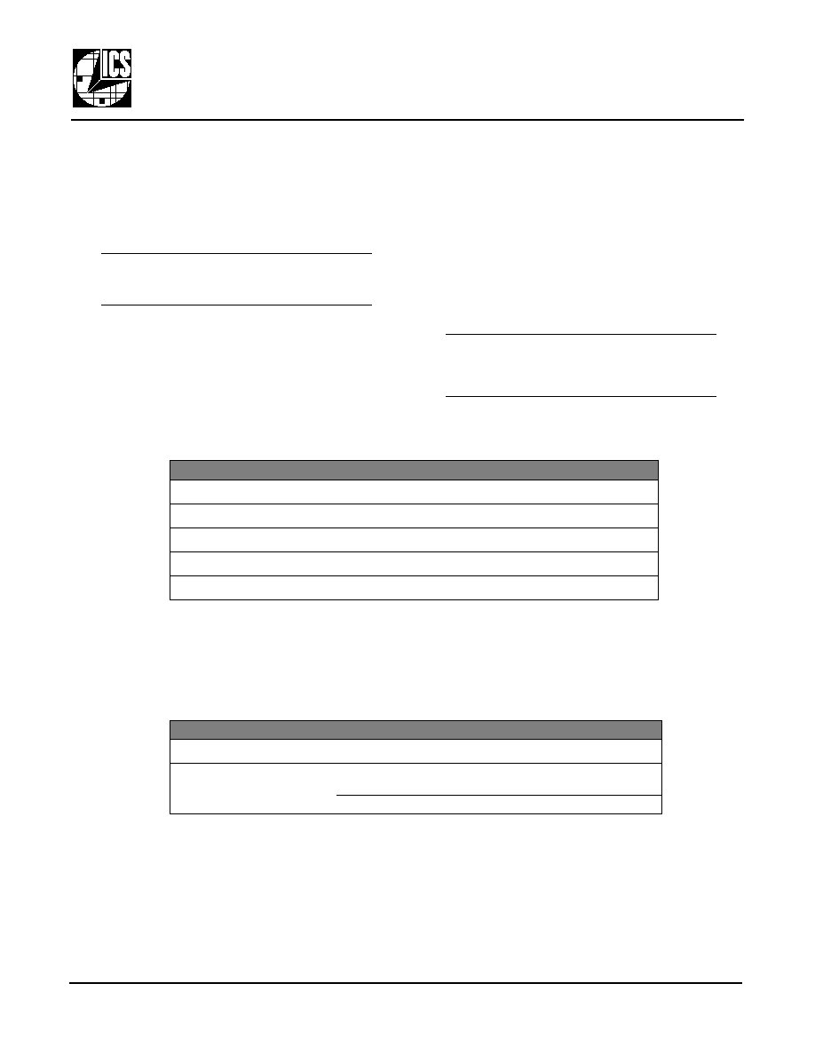
P
IN
A
SSIGNMENT
(9 x 9 mm SMT)
Figure 1: Pin Assignment
S
IMPLIFIED
B
LOCK
D
IAGRAM
Figure 2: Simplified Block Diagram
Example Output Frequency Configurations
Ref Clock
Frequency
(MHz)
PLL
Ratio
Output
Frequency
1
(MHz)
Note 1: Specify output clock frequency at time of order
Application
20
25/4
125.00
GbE
25
156.25
10GbE
30
187.50
12GbE
Table 1: Example Output Frequency Configurations
M 9 0 2 - 0 1
( T o p V i e w )
1
2
3
4
5
6
7
8
9
X
T
A
L
_1
/
R
E
F_
IN
GN
D
ST
O
P
EX
T
_
C
L
K
EN
_
E
XT
_
C
L
K
NC
NC
NC
VC
C
NC
NC
nFOUT1
FOUT1
GND
nFOUT0
FOUT0
VCC
GND
XTAL_2
NC
NC
NC
NC
VCC
DNC
DNC
DNC
nO
P_IN
OP
_
O
UT
VC
nVC
nO
P_O
U
T
OP
_
I
N
GND
GND
GND
19
20
21
22
23
24
25
26
27
28
29
30
31
32
33
34
35
36
18
17
16
15
14
13
12
11
10
M902-01
XTAL
OSC
O
1
External
Crystal
or
Reference
Clock Input
(e.g., 25 or 30MHz)
LVPECL
Output
Clock Pairs
(e.g., 156.25
or 187.50MHz)
Divider
External
Clock
Input
External
Clock
Select
Output
Clock STOP
Control
VSCO
Frequency
Multiplying
PLL
External
Loop Filter
M902-01 VCSO Based GbE Clock Generator

M902-01 Datasheet Rev 2.1
2 of 8
Revised 24Jun2004
I n t e g r a t e d C i r c u i t S y s t e m s , I n c .
N e t w o r k i n g & C o m m u n i c a t i o n s
w w w. i c s t . c o m
t e l ( 5 0 8 ) 8 5 2 - 5 4 0 0
Integrated
Circuit
Systems, Inc.
M902-01
VCSO B
ASED
G
B
E C
LOCK
G
ENERATOR
P r o d u c t D a t a S h e e t
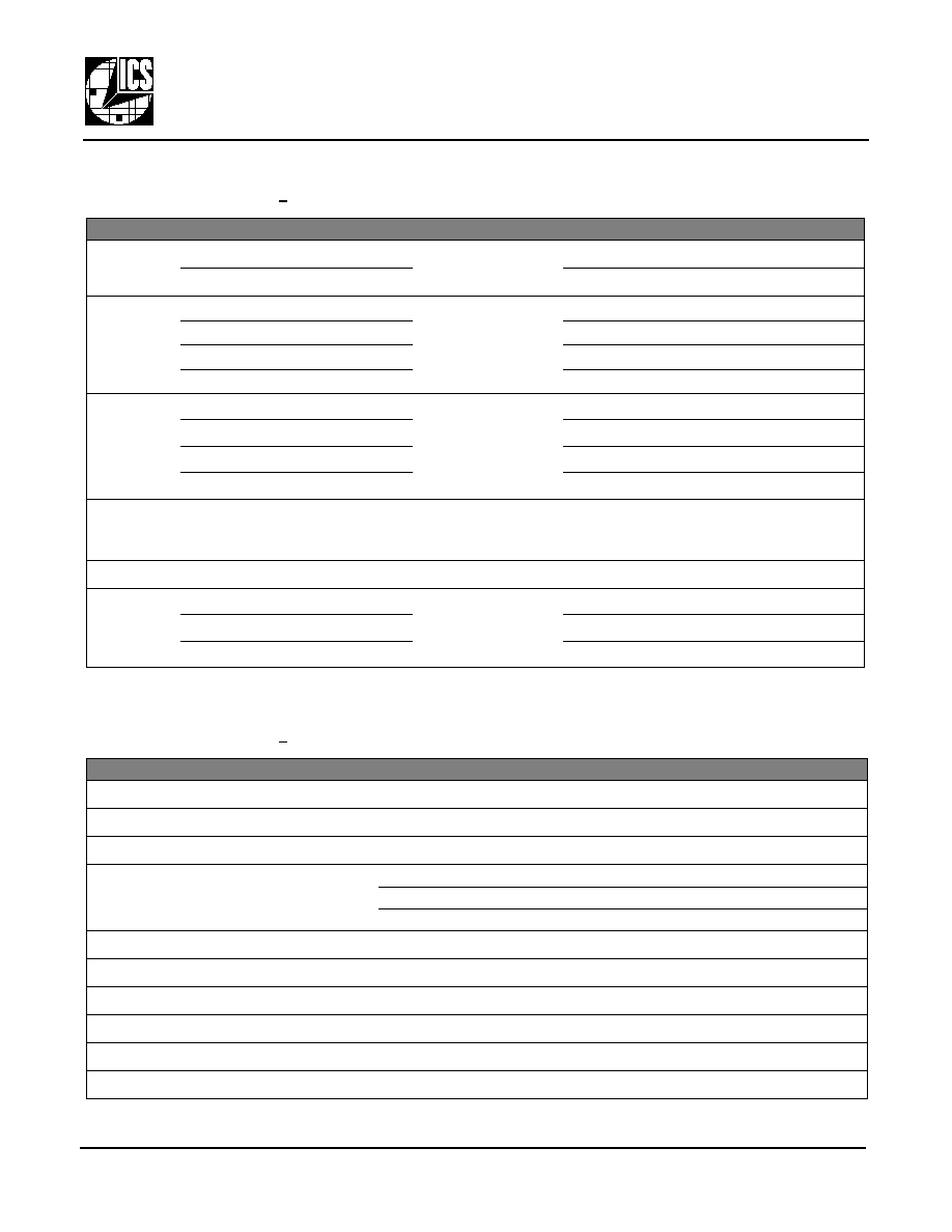
D
ETAILED
B
LOCK
D
IAGRAM
Figure 3: Detailed Block Diagram
P
IN
D
ESCRIPTIONS
Number
Name
I/O
Configuration
Description
1, 2, 3, 10, 14, 26 GND
Ground
Power supply ground connections.
4
9
OP_IN
nOP_IN
Input
External loop filter connections. See Figure 5,
External Loop Filter, on pg. 4.
5
8
nOP_OUT
OP_OUT
Output
6
7
nVC
VC
Input
11, 19, 33
VCC
Power
Power supply connection, connect to +
3.3
V.
12
13
FOUT0
nFOUT0
Output
No internal terminator
Clock output pairs, differential LVPECL output
(
156.25
MHz for the
M902-01-156.2500
)
15
16
FOUT1
nFOUT1
17, 18
NC
No internal connection
20, 21, 22
29, 30, 31, 32
23
EN_EXT_CLK
Input
Internal pull-down resistor
1
Note 1: For typical value of internal pull-down resistor, see DC Characteristics, Pull-down on pg. 6.
Logic
1
enables the
EXT_CLK
input.
Use Logic
0
for normal operation.
24
EXT_CLK
Input
External clock feed-through:
0
to
200
MHz
25
STOP
Input
Internal pull-down resistor
1
Logic
1
stops clock outputs.
Use Logic
0
for normal operation.
27
XTAL_1 / REF_IN
Input
External crystal connection. Also accepts
LVCMOS/LVTTL compatible clock source.
28
XTAL_2
Input
External crystal connection. Leave unconnected
when driving pin
27
with external clock reference.
34, 35, 36
DNC
Do Not Connect.
Table 2: Pin Descriptions
M902-01
XTAL_2
XTAL_1 / REF_IN
XTAL
OSC
EXT_CLK
EN_EXT_CLK
STOP
R Divider
R = 4
Phase
Detector
VCSO
SAW Delay Line
Phase
Shifter
VCSO
C
POST
C
POST
VC
nVC
R
POST
nOP_OUT
OP_OUT
R
POST
R
LOOP
R
LOOP
C
LOOP
C
LOOP
R
IN
R
IN
OP_IN
nOP_IN
Loop Filter
Amplifier
External
Loop Filter
Components
M Divider
M = 25
Phase Locked Loop (PLL)
O
1
FOUT1
nFOUT1
FOUT0
nFOUT0

M902-01 Datasheet Rev 2.1
3 of 8
Revised 24Jun2004
I n t e g r a t e d C i r c u i t S y s t e m s , I n c .
N e t w o r k i n g & C o m m u n i c a t i o n s
w w w. i c s t . c o m
t e l ( 5 0 8 ) 8 5 2 - 5 4 0 0
M902-01
VCSO B
ASED
G
B
E C
LOCK
G
ENERATOR
P r o d u c t D a t a S h e e t
Integrated
Circuit
Systems, Inc.
F
UNCTIONAL
D
ESCRIPTION
The M902-01 is a PLL (Phase Locked Loop) based
clock generator that generates output clocks
synchronized to an input reference clock.
The M902-01 combines the flexibility of a VCSO
(Voltage Controlled SAW Oscillator) with the stability of
a crystal oscillator.
Input Reference
The input reference can either be an external, discrete
crystal or a stable external clock source such as a
packaged (temperature-compensated) crystal
oscillator.
�
If an external crystal is used with the on-chip crystal
oscillator circuit (XTAL OSC), the external crystal
should be a parallel-resonant, fundamental mode
crystal. Apply it to the
XTAL_1 / REF_IN
and
XTAL_2
input
pins. External crystal load trim capacitors are also
required. (See "Crystal Specifications" on pg. 4.)
�
If an external LVCMOS/LVTTL clock source is used,
apply it to the
XTAL_1 / REF_IN
input pin.
In either case, the reference clock is supplied to the
phase detector of the PLL. The M902-01 includes a
reference divider that divides the input reference
frequency by a fixed value "R" and provides the result to
the phase detector.
The EX_CLK pin is available for a clock feed-through
mode for testing. See "External Clock Feed-through"
on pg. 3.
The PLL
The PLL (Phase Locked Loop) includes the phase
detector, the VCSO, a feedback divider (labeled
"M Divider"), and a reference divider ("R Divider").
The feedback divider divides the VCSO output
frequency by a fixed value "M" to match the reference
frequency provided to the phase detector by the
reference divider.
By controlling the frequency and phase of the VCSO,
the phase detector precisely locks the frequency and
phase of the feedback divider output to that of the
reference divider output.
The relationship between the VCSO output frequency,
the M Divider, the R Divider and the input reference
frequency is defined as follows:
For the
M902-01-156.2500 (see "Ordering Information" on pg. 8):
�
VCSO output frequency = 156.25MHz
�
Input reference frequency = 25MHz
�
M=25
�
R= 4
Therefore, for the
M902-01-156.2500
:
25
156.25MHz = 25MHz
4
The product of the input crystal frequency and
falls within the lock range of the VCSO.
External Clock Feed-through
The
EXT_CLK
pin provides an input for an external
single-ended clock that directly drives the LVPECL
clock outputs. This pin is intended for system debugging
and performance evaluation..
STOP Clock
The
STOP
pin puts the output clock into a static condition.
EN_EXT_CLK
Logic
1
enables the
EXT_CLK
input.
Use Logic
0
for normal operation.
EXT_CLK
Apply an external LVCMOS/LVTTL clock source
for
0
to
200
MHz feed-through operation.
Leave inactive for normal operation.
1
Note 1: In applications where EXT_CLK is active while the SAW PLL
signal path is enabled, it is necessary to gate the EXT_CLK to
minimize jitter in the LVPECL output pairs. See the PCB Design
Guidelines for ICS SAW PLLs application note at
www.icst.com/products/appnotes/M000-AN-001.PCBdesign.pdf
Logic 1 Output clocks are static
Logic 0 Output clocks enabled for normal operation
Fvcso
Fxtal
M
R
-----
�
=
----------
�
M
R
-----

M902-01 Datasheet Rev 2.1
4 of 8
Revised 24Jun2004
I n t e g r a t e d C i r c u i t S y s t e m s , I n c .
N e t w o r k i n g & C o m m u n i c a t i o n s
w w w. i c s t . c o m
t e l ( 5 0 8 ) 8 5 2 - 5 4 0 0
Integrated
Circuit
Systems, Inc.
M902-01
VCSO B
ASED
G
B
E C
LOCK
G
ENERATOR
P r o d u c t D a t a S h e e t
A
PPLICATION
I
NFORMATION
This section includes information on the optional
external crystal and on the external loop filter.
The subsections on the loop filter provide example
component values and also briefly describe the SAW
PLL simulator tool and additional application
information available at www.icst.com.
External Crystal Specifications
If an external crystal is used with the on-chip crystal
oscillator circuit (XTAL OSC), the external crystal
should have the following general specifications:
The external crystal will be applied to the
XTAL_1 / REF_IN
and
XTAL_2
input pins. External crystal load capacitors
are also required.
Recommended External Crystal Configuration
Figure 4: Recommended External Crystal Configuration
XTAL= 25 or 30 MHz, Load Capacitance Specification = 18 pF
C1
= 27 pF
C2
= 33 pF
External load capacitors C1 and C2 present a load of 15 pf
to the crystal (they are seen in series by the crystal through
the common ground connection). With the additional of PCB
trace capacitance and M902-01 input capacitance, the total
load to the crystal is about 18 pf.
External Loop Filter
To provide stable PLL operation, and thereby a low jitter
output clock, the M902-01 requires the use of an
external loop filter. This is provided via the provided
filter pins (see Figure 5).
Figure 5: External Loop Filter
The loop filter is implemented as a differential circuit
to minimize system noise interference. Due to the
differential signal path design, the implementation
requires two identical complementary RC filters as
shown here. See Table 4, External Loop Filter
Component Values, below.
Refer to the M902-01 product web page at
www.icst.com/products/summary/m902-01.htm for
additional product information.
Crystal Specifications
Parameter
Min Typ Max Unit
Crystal Type
AT-cut quartz
Mode of Oscillation
Fundamental
f
0
Nominal Frequency Range
16
40
MHz
f/f
0
Frequency Tolerance @
+25
o
C
1
Note 1: These frequency tolerance specifications are suitable for
a
�100 ppm clock output frequency requirement.
�
15
ppm
f/f
C
/ T
A
Frequency Stability
-40 to +85
o
C
1
�
50
ppm
f/f
0
/ y Aging, per year (first) @
+25
o
C
1
�
5
ppm
ESR
Equivalent Series Resistance
50
C
S
Shunt Capacitance
7
pF
Spurious Response (non-harmonic)
-
40
dBc
C
L
Load Capacitance,
parallel load resonant
16
32
pF
P
0
Drive Level
0.1
1.0
mW
Table 3: External Loop Filter Component Values
XTAL_2
XTAL
XTAL OSC
M9xx-0x
XTAL_1 / REF_IN
C1
C2
M902-01
External Loop Filter Component Values
PLL Bandwidth
(
kHz
)
Damping
Factor
R loop
(
k
)
C loop
(
�F
)
R post
(
k
)
C post
(
pF
)
0.5
3.0
1.5
4.70
20
150
1.5
1
Note 1: Optimum loop bandwidth when using an external reference
crystal. Will help to attenuate interference on the crystal's
sinusoidal clock waveform and therefore will minimize
device output clock jitter.
3.3
4.7
1.00
10
150
2.1
2
Note 2: Alternative loop filter setting when using an external refer-
ence crystal. Smaller C loop lowers loop damping factor with
negligible increase in output jitter.
1.1
4.7
0.10
10
150
6.4
4.5
20.0
0.10
20
270
10.6
3
Note 3: Optimum loop bandwidth when using an external reference
crystal oscillator. The square wave clock reference does not
require as much jitter attenuation, which allows for a wider
loop bandwidth and improved system noise tolerance.
4.2
33.0
0.03
20
120
Table 4: External Loop Filter Component Values
C
POST
C
POST
VC
nVC
R
POST
nOP_OUT
OP_OUT
R
POST
R
LOOP
R
LOOP
C
LOOP
C
LOOP
OP_IN
nOP_IN
6
7
5
4
9
8
M902-01 Datasheet Rev 2.1
5 of 8
Revised 24Jun2004
I n t e g r a t e d C i r c u i t S y s t e m s , I n c .
N e t w o r k i n g & C o m m u n i c a t i o n s
w w w. i c s t . c o m
t e l ( 5 0 8 ) 8 5 2 - 5 4 0 0
M902-01
VCSO B
ASED
G
B
E C
LOCK
G
ENERATOR
P r o d u c t D a t a S h e e t
Integrated
Circuit
Systems, Inc.
PLL Simulator Tool Available
A free PC software utility is available on the ICS website
(www.icst.com). The M2000 Timing Modules PLL
Simulator is a downloadable application that simulates
PLL jitter and wander transfer characteristics. This
enables the user to set appropriate external loop
component values in a given application.
Refer to the SAW PLL Simulator Software web page at
www.icst.com/products/calculators/m2000filterSWdesc.htm
for additional information.
SAW PLL Application Notes Available
The ICS web site (www.icst.com) also has application
notes on:
�
PCB layout guidelines (including special detailed
instructions for preventing issues such as external
reference crosstalk)
�
Any new special device application details that may
become available
�
Instructions for using PLL simulator software
�
Guidelines for PCB fabrication (including recom-
mended PCB footprint, solder mask, and furnace
profile)
Refer to the SAW PLL Application Notes web page at
www.icst.com/products/appnotes/SawPllAppNotes.htm
for application notes and any additional product
information that may become available.
A
BSOLUTE
M
AXIMUM
R
ATINGS
1
Symbol Parameter
Rating
Unit
V
I
Input Voltage
-
0.5
to V
CC
+
0.5
V
V
O
Output Voltage
-
0.5
to V
CC
+
0.5
V
I
O
Output Current
25
mA
V
CC
Power Supply Voltage
4.6
V
T
S
Storage Temperature
-
45
to +
100
o
C
Table 5: Absolute Maximum Ratings
Note 1: Stresses beyond those listed under Absolute Maximum Ratings may cause permanent damage to the
device. These ratings are stress specifications only. Functional operation of product at these conditions
or any conditions beyond those listed in Recommended Conditions of Operation, DC Characteristics, or
AC Characteristics is not implied. Exposure to absolute maximum rating conditions for extended periods
may affect product reliability.
R
ECOMMENDED
C
ONDITIONS
OF
O
PERATION
Symbol Parameter
Min
Typ
Max
Unit
V
CC
Positive Supply Voltage
3.135
3.3
3.465
V
T
A
Ambient Operating Temperature
Commercial
0
+
70
o
C
Industrial
-40
+
85
o
C
Table 6: Recommended Conditions of Operation
M902-01 Datasheet Rev 2.1
6 of 8
Revised 24Jun2004
I n t e g r a t e d C i r c u i t S y s t e m s , I n c .
N e t w o r k i n g & C o m m u n i c a t i o n s
w w w. i c s t . c o m
t e l ( 5 0 8 ) 8 5 2 - 5 4 0 0
Integrated
Circuit
Systems, Inc.
M902-01
VCSO B
ASED
G
B
E C
LOCK
G
ENERATOR
P r o d u c t D a t a S h e e t
E
LECTRICAL
S
PECIFICATIONS
DC Characteristics
Unless stated otherwise, V
CC
= 3.3V +5%,T
A
= 0
o
C to +70
o
C (commercial)
1
, T
A
= -40
o
C to +85
o
C (industrial)
1
, Output Frequency=156.25MHz
1
,
LVPECL outputs terminated with 50
to V
CC
- 2V
Symbol Parameter
Min
Typ
Max
Unit
Power Supply
V
CC
Positive Supply Voltage
3.135
3.3
3.465
V
I
CC
Power Supply Current
300
mA
Logic Inputs
V
IH
Input High Voltage
EN_EXT_CLK, EXT_CLK,
STOP
2
V
cc
+
0.3
V
V
IL
Input Low Voltage
-
0.3
0.8
V
I
IH
Input High Current
150
�A
I
IL
Input Low Current
-
5.0
�A
Reference
Clock
Input
V
IH
Input High Voltage
XTAL_1 / REF_IN
(XTAL_2 disconnected)
(V
cc
/
2
) +
0.5
V
cc
+
0.3
V
V
IL
Input Low Voltage
-
0.3
(V
cc
/
2
) -
0.5
V
I
IH
Input High Current
150
�A
I
IL
Input Low Current
-
5.0
�A
All Inputs
C
IN
Input Capacitance, All Inputs
EN_EXT_CLK, EXT_CLK,
STOP,
XTAL_1 / REF_IN, XTAL_2
4
pF
Pull-down
R
pulldown
Internal Pull-down Resistor
EN_EXT_CLK, STOP
51
k
Differential
Output
V
OH
Output High Voltage
FOUT, nFOUT (0-1)
V
cc
-
1.4
V
cc
-
1.0
V
V
OL
Output Low Voltage
V
cc
-
2.0
V
cc
-
1.7
V
V
P
-
P
Peak to Peak Output Voltage
0.5
0.85
V
Table 7: DC Characteristics
Note 1: See Ordering Information on pg. 8
AC Characteristics
Unless stated otherwise, V
CC
= 3.3V +5%,T
A
= 0
o
C to +70
o
C (commercial)
1
, T
A
= -40
o
C to +85
o
C (industrial)
1
, Output Frequency=156.25MHz
1
,
LVPECL outputs terminated with 50
to V
CC
- 2V
Symbol Parameter
Min
Typ
Max
Unit
Test Conditions
F
OUT
Output Frequency Range
125
156.25
190
MHz
F
IN
Nominal Input Frequency,
XTAL_1 / REF_IN
25
MHz
APR
VCSO Pull-Range
�
100
�
150
ppm
n
Single Side Band
Phase Noise
@
156.25
MHz
1
kHz Offset
-
90
dBc/Hz
10
kHz Offset
-
110
dBc/Hz
100
kHz Offset
-
135
dBc/Hz
J(t)
Jitter (rms)
0.5
1.0
ps
12
kHz to
20
MHz
t
DC
Output Duty Cycle, High Time
45
50
55
%
t
R
Output Rise Time
FOUT, nFOUT (0-1)
350
450
550
ps
20
% to
80
%
t
F
Output Fall Time
FOUT, nFOUT (0-1)
350
450
550
ps
20
% to
80
%
t
S
Output Skew
Between Any Pair
100
ps
EXT_CLK
Frequency
EXT_CLK
0
200
MHz
Table 8: AC Characteristics
Note 1: See Ordering Information on pg. 8

M902-01 Datasheet Rev 2.1
7 of 8
Revised 24Jun2004
I n t e g r a t e d C i r c u i t S y s t e m s , I n c .
N e t w o r k i n g & C o m m u n i c a t i o n s
w w w. i c s t . c o m
t e l ( 5 0 8 ) 8 5 2 - 5 4 0 0
M902-01
VCSO B
ASED
G
B
E C
LOCK
G
ENERATOR
P r o d u c t D a t a S h e e t
Integrated
Circuit
Systems, Inc.
D
EVICE
P
ACKAGE
-
9 x 9mm
C
ERAMIC
L
EADLESS
C
HIP
C
ARRIER
Mechanical Dimensions:
Figure 6: Device Package - 9 x 9mm Ceramic Leadless Chip Carrier
Refer to the M902-01 product web page at
www.icst.com/products/summary/m902-01.htm
for recommended PCB footprint, solder mask,
furnace profile, and related information.

M902-01 Datasheet Rev 2.1
8 of 8
Revised 24Jun2004
I n t e g r a t e d C i r c u i t S y s t e m s , I n c .
N e t w o r k i n g & C o m m u n i c a t i o n s
w w w. i c s t . c o m
t e l ( 5 0 8 ) 8 5 2 - 5 4 0 0
Integrated
Circuit
Systems, Inc.
While the information presented herein has been checked for both accuracy and reliability, Integrated Circuit Systems (ICS)
assumes no responsibility for either its use or for the infringement of any patents or other rights of third parties, which would
result from its use. No other circuits, patents, or licenses are implied. This product is intended for use in normal commercial
applications. Any other applications such as those requiring extended temperature range, high reliability, or other extraordinary
environmental requirements are not recommended without additional processing by ICS. ICS reserves the right to change any
circuitry or specifications without notice. ICS does not authorize or warrant any ICS product for use in life support devices or
critical medical instruments.
M902-01
VCSO B
ASED
G
B
E C
LOCK
G
ENERATOR
P r o d u c t D a t a S h e e t
O
RDERING
I
NFORMATION
Part Numbering Scheme
Figure 7: Part Numbering Scheme
Consult factory for frequency availability.
Part Number:
M902-
01
-
xxx.xxxx
Output Frequency (MHz)
"
- " =
0 to +70
o
C (commercial)
See Table 9, right. Consult ICS for other frequencies.
I
=
- 40 to +85
o
C (industrial)
Temperature
Device Number
Example Part Numbers
Output Freq.
(MHz)
Temperature Order Part Number
125.00
commercial
M902-01
- 125.0000
industrial
M902-01I125.0000
156.25
commercial
M902-01
- 156.2500
industrial
M902-01I156.2500
187.50
commercial
M902-01
- 187.5000
industrial
M902-01I187.5000
Table 9: Example Part Numbers