 | –≠–ª–µ–∫—Ç—Ä–æ–Ω–Ω—ã–π –∫–æ–º–ø–æ–Ω–µ–Ω—Ç: MK1705A | –°–∫–∞—á–∞—Ç—å:  PDF PDF  ZIP ZIP |

PLL Clock
Synthesis and
Spread Spectrum
Circuitry
MK1705A
ATI Low EMI Clock Generator
MDS 1705A B
1
Revision 8090
Printed 8/9/00
Integrated Circuit Systems, Inc. ∑525 Race Street∑San Jose∑CA ∑ 95126 ∑ (408)295-9800tel ∑ www.icst.com
ICRO
C
LOCK
The MK1705A generates a low EMI output clock
from a clock or crystal input. The part is designed
to dither the LCD interface clock or other clocks
for ATI's flat panel graphics controllers. The
device uses ICS/MicroClock's proprietary mixture
of analog and digital Phase-Locked Loop (PLL)
technology to synthesize the frequency, and our
patented technique to spread the frequency
spectrum of the output, thereby reducing the
frequency amplitude peaks by several dB.
The MK1705A is designed to have the output
spread centered around the input frequency. Refer
to the MK1704A for spreading down from the
input frequency, or the MK1714-0x for a crystal
input and the widest selection of spread rates and
multipliers.
We offer many other clocks for computers and
computer peripherals. Consult us when you need
to remove crystals and oscillators from your board.
Block Diagram
Description
Features
∑ Packaged in 8 pin SOIC
∑ Provides a spread spectrum output clock
∑ Supports ATI's flat panel controllers
∑ Accepts a clock input, provides same frequency
dithered output
∑ Good for all VGA modes from 40 to 167 MHz
∑ Peak reduction by 7dB - 14 dB typical on 3rd-
19th odd harmonics
∑ Low EMI feature can be disabled
∑ 3.3 V or 5 V ±10% supply voltage
∑ Advanced, low power CMOS process
Input
Buffer
VDD GND
S1
Output
Buffer
Clock Out
Input Clock
Low EMI Enable
S0
Power Down
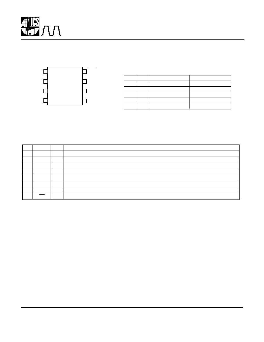
MK1705A
ATI Low EMI Clock Generator
MDS 1705A B
2
Revision 8090
Printed 8/9/00
Integrated Circuit Systems, Inc. ∑525 Race Street∑San Jose∑CA ∑ 95126 ∑ (408)295-9800tel ∑ www.icst.com
ICRO
C
LOCK
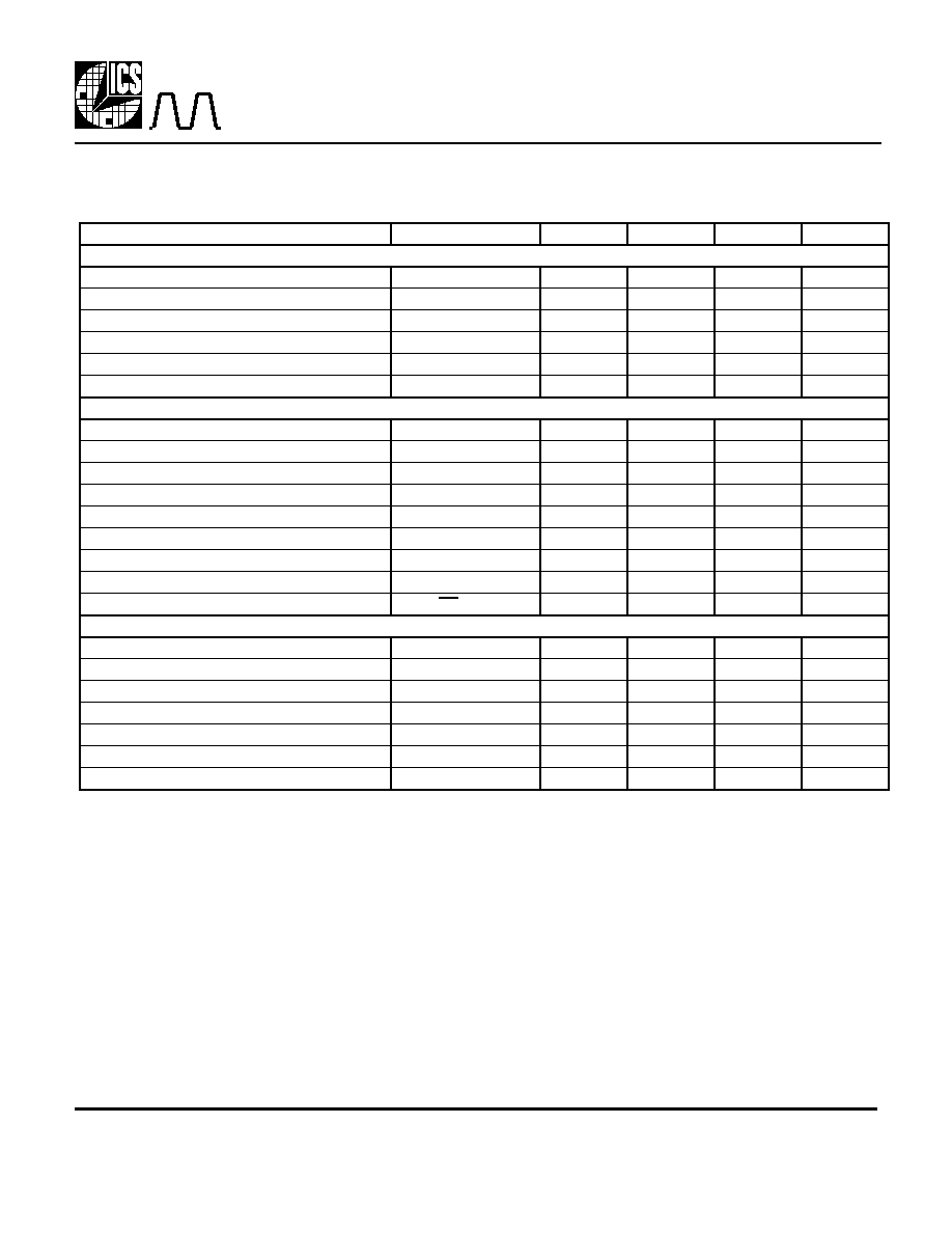
Pin Assignment
1
8
2
3
4
7
6
5
ICLK
S0
GND
PD
VDD
LEE
8 pin SOIC
CLK
S1
External Components
A minimum number
of external components are required for proper operation. A decoupling capacitor of
0.01µF should be connected between VDD and GND on pins 2 and 3 as close to the chip as possible, and
a 33
series terminating resistor may be used on the clock output if the trace is longer than 1 inch.
Pin #
Name
Type Description
1
ICLK
I
Connect to graphics input clock
2
VDD
P
Connect to +3.3V or +5V.
3
GND
P
Connect to ground.
4
CLK
O
Spread spectrum Clock Output per table above.
5
LEE
I
Low EMI Enable. Turns on the spread spectrum when high. Internal pull-up.
6
S1
I
Frequency Select 1 Input. Selects spread amount and CLK range per table above. Internal pull-up.
7
S0
I
Frequency Select 0 Input. Selects spread amount and CLK range per table above. Internal pull-up.
8
PD
I
Power Down. Stops output low when this pin is low. Internal pull-up.
Pin Descriptions
Key: I = Input, O = output, P = power supply connection
S1
S0
Input/Output Range
Frequency spread
pin 6 pin 7
pin 1/pin 4
vs. CLK
0
0
40 to 167 MHz
Center ±1.25%
0
1
60 to 167 MHz
Center ±0.5%
1
0
Test
Test
1
1
40 to 100 MHz
Center ±1%
Clock Output Select Table
MK1705A
ATI Low EMI Clock Generator
MDS 1705A B
3
Revision 8090
Printed 8/9/00
Integrated Circuit Systems, Inc. ∑525 Race Street∑San Jose∑CA ∑ 95126 ∑ (408)295-9800tel ∑ www.icst.com
ICRO
C
LOCK
Notes:
1. Stresses beyond those listed under Absolute Maximum Ratings could cause permanent damage to the device. Prolonged exposure
to levels above the operating limits but below the Absolute Maximums may affect device reliability.
2. Typical values are at 25∞C.
Electrical Specifications
Parameter
Conditions
Minimum
Typical
Maximum
Units
ABSOLUTE MAXIMUM RATINGS (note 1)
Supply Voltage, VDD
Referenced to GND
7
V
Inputs
Referenced to GND
-0.5
VDD+.5V
V
Clock Outputs
Referenced to GND
-0.5
VDD+.5V
V
Ambient Operating Temperature
0
70
∞C
Soldering Temperature
Max of 10 seconds
260
∞C
Storage temperature
-65
150
∞C
DC CHARACTERISTICS (at 5.0V unless otherwise noted)
DC CHARACTERISTICS (at 5.0V unless otherwise noted)
Operating Voltage, VDD
3
5.5
V
Input High Voltage, VIH, ICLK
(VDD/2)+1
VDD/2
V
Input Low Voltage, VIL, ICLK
VDD/2
(VDD/2)-1
V
Output High Voltage, VOH, CMOS
IOH=-4mA
VDD-0.4
V
Output High Voltage, VOH
IOH=-25mA
2.4
V
Output Low Voltage, VOL
IOL=25mA
0.4
V
Operating Supply Current, IDD, 5V
No Load
20
mA
Operating Supply Current, IDD, 3.3V
No Load
15
mA
Input Capacitance
S0, S1, PD, LEE pins
7
pF
AC CHARACTERISTICS (at 5.0V unless otherwise noted)
AC CHARACTERISTICS (at 5.0V unless otherwise noted)
Input Clock Frequency
40 - 167
MHz
Input Clock Duty Cycle
Time above VDD/2
20
80
%
Output Clock Rise Time
0.8 to 2.0V
1.5
ns
Output Clock Fall Time
2.0 to 0.8V
1.5
ns
Output Clock Duty Cycle
Time above 1.5V
40
50
60
%
Output Clock Frequency Variation from Mean
LEE high
±0.5 to ±1.25
%
EMI Peak Frequency Reduction
3rd-19th odd harmonics
7 to 14
dB
MK1705A
ATI Low EMI Clock Generator
MDS 1705A B
4
Revision 8090
Printed 8/9/00
Integrated Circuit Systems, Inc. ∑525 Race Street∑San Jose∑CA ∑ 95126 ∑ (408)295-9800tel ∑ www.icst.com
ICRO
C
LOCK
While the information presented herein has been checked for both accuracy and reliability, ICS MicroClock assumes no responsibility for either its use or for the infringement of
any patents or other rights of third parties, which would result from its use. No other circuits, patents, or licenses are implied. This product is intended for use in normal
commercial applications. Any other applications such as those requiring extended temperature range, high reliability, or other extraordinary environmental requirements are not
recommended without additional processing by ICS MicroClock. ICS MicroClock reserves the right to change any circuitry or specifications without notice. ICS MicroClock
does not authorize or warrant any ICS MicroClock product for use in life support devices or critical medical instruments.
Ordering Information
Part/Order Number
Marking
Package
Temperature
MK1705A
MK1705A
8 pin SOIC
0 to 70 ∞C
MK1705ATR
MK1705A
Add tape and reel
0 to 70 ∞C
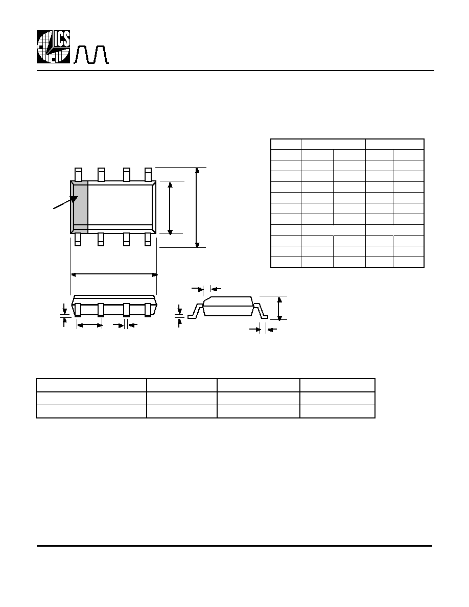
Package Outline and Package Dimensions
(
For current dimensional specifications, see JEDEC Publication No. 95.)
B
D
E
H
e
A1
C
A
h x 45∞
L
INDEX
AREA
8 pin SOIC
Inches
Inches
Millimeters
Millimeters
Symbol
Min
Max
Min
Max
A
0.0532
0.0688
1.35
1.75
A1
0.0040
0.0098
0.10
0.24
B
0.0130
0.0200
0.33
0.51
C
0.0075
0.0098
0.19
0.24
D
0.1890
0.1968
4.80
5.00
E
0.1497
0.1574
3.80
4.00
e
.050 BSC
.050 BSC
1.27 BSC
1.27 BSC
H
0.2284
0.2440
5.80
6.20
h
0.0099
0.0195
0.25
0.50
L
0.0160
0.0500
0.41
1.27