 | –≠–ª–µ–∫—Ç—Ä–æ–Ω–Ω—ã–π –∫–æ–º–ø–æ–Ω–µ–Ω—Ç: MK1709 | –°–∫–∞—á–∞—Ç—å:  PDF PDF  ZIP ZIP |

MK1709
MDS 1709 D
1
Revision 031204
Integrated Circuit Systems, Inc.
525 Race Street, San Jose, CA 95126
tel (408) 297-1201
www.icst.com
Low EMI Clock Generator
Description
The MK1709 generates a low EMI output clock from a
clock input. The part is designed to dither the LCD
interface clock for flat panel graphics controllers. The
device uses ICS' proprietary mix of analog and digital
Phase Locked Loop (PLL) technology to spread the
frequency spectrum of the output, thereby reducing the
frequency amplitude peaks by several dB.
The MK1709 offers centered spread from a high speed
clock input. Refer to the MK1714-01/02 for a crystal
input and the widest selection of input frequencies and
multipliers.
ICS offers many other clocks for computers and
computer peripherals. Consult us when you need to
remove crystals and oscillators from your board.
Features
∑
Packaged in 8-pin SOIC (MK1709S) and in 8-pin
TSSOP (MK1709AG)
∑
8-pin TSSOP available in lead (Pb) free package
∑
Provides a spread spectrum output clock
∑
Supports flat panel controllers
∑
Guaranteed to +85
∞C operation
∑
Accepts a clock input, provides same frequency
dithered output
∑
Good for all VGA modes from 80 to 167 MHz
∑
Peak reduction by 7dB - 14dB typical on 3rd - 19th
odd harmonics
∑
Low EMI feature can be disabled
∑
Includes power-down
∑
Operating voltage of 3.3 V
∑
Advanced, low-power CMOS process
Block Diagram
PLL Clock
Synthesis
and Spread
Spectrum
Circuitry
ICLK
Input
Buffer
S0
Low EMI Enable
Clock Out
GND
VDD
S1
S2
Low EMI Clock Generator
MDS 1709 D
2
Revision 031204
Integrated Circuit Systems, Inc.
525 Race Street, San Jose, CA 95126
tel (408) 297-1201
www.icst.com
MK1709
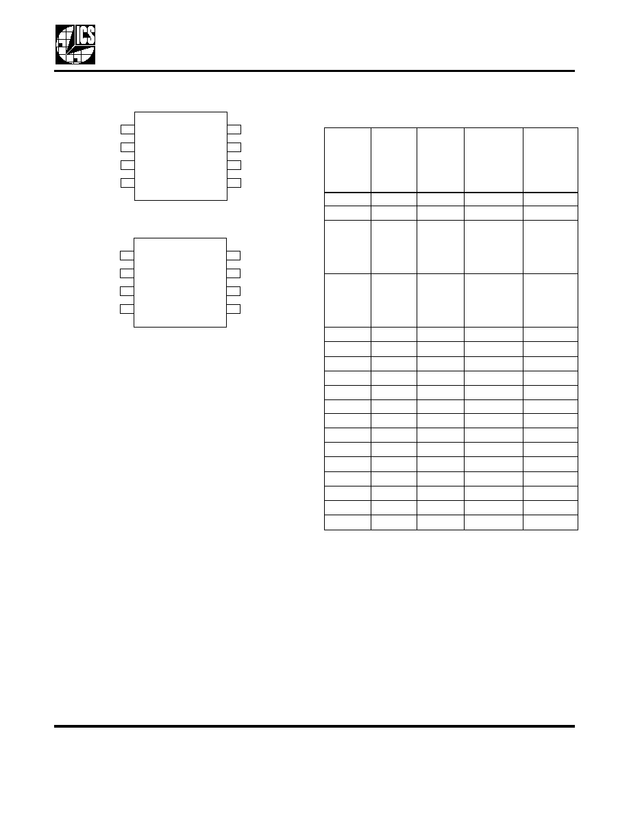
Pin Assignment
Spread Percentage and Direction
Select Table
0 = connect to GND
M = unconnected (floating) has internal Pull up resistor
to VDD and is considered as a 1 state
1 = connect directly to VDD
ICLK
VDD
GND
S1
CLK
S0
LEE
S2
1
2
3
4
8
7
6
5
8-pin SOIC (MK1709S)
CLK
VDD
GND
S1
ICLK
S0
LEE
S2
1
2
3
4
8
7
6
5
8-pin TSSOP (MK1709AG)
S2
Pin 8
(1709S)
Pin 6
(1709AG)
S1
Pin 7
(1709S)
Pin 5
(1709AG)
S0
Pin 6
(1709S)
Pin 4
(1709AG)
Frequency
Range
Spread
Percentage
(%)
0
0
0
40-50
±0.9
0
0
M
40-50
±0.7
0
0
1
40-50
(MK1709S)
25-50
(MK1709AG)
±0.8
0
M
0
40-50
(MK1709S)
25-50
(MK1709AG)
±0.6
0
M
M
40-50
±1.1
0
M
1
50 -100
±0.6
0
1
0
50 -100
±0.7
0
1
M
50 -100
±0.8
0
1
1
Power Down
--
1
0
0
50 -100
±0.9
1
0
M
50 -100
±1.1
1
0
1
100-165
±0.7
1
M
0
100-165
±0.6
1
M
M
100-165
±1.1
1
M
1
100-165
±1.35
1
1
0
100-165
±0.8
1
1
M
100-165
±0.9
1
1
1
Power Down
--

Low EMI Clock Generator
MDS 1709 D
3
Revision 031204
Integrated Circuit Systems, Inc.
525 Race Street, San Jose, CA 95126
tel (408) 297-1201
www.icst.com
MK1709
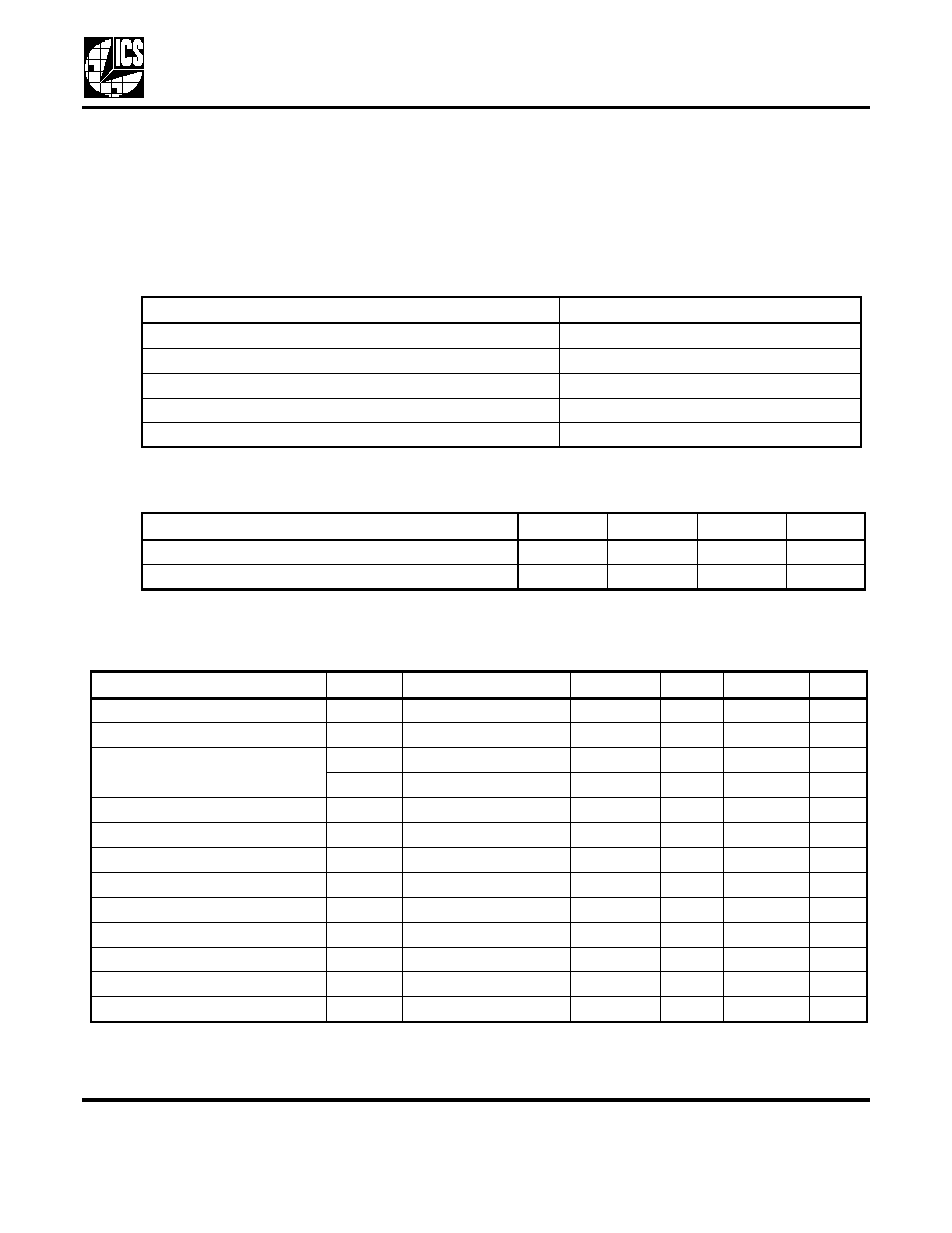
Pin Descriptions
(MK1709S)
Pin Descriptions
(MK1709AG)
Pin
Number
Pin
Name
Pin Type
Pin Description
1
ICLK
Input
Connect to graphics input clock.
2
VDD
Power
Connect to +3.3 V.
3
GND
Power
Connect to ground.
4
CLK
Output
Spread spectrum clock output per table above.
5
LEE
Input
Low EMI enable. Turns on spread spectrum when high. Internal pull-up resistor.
6
S0
Input
Function select 0 input. Selects spread amount and direction per table above.
Internal mid-level.
7
S1
Input
Function select 1 input. Selects spread amount and direction per table above.
Internal mid-level.
8
S2
Input
Function select 2 input. Selects spread amount and direction per table above.
Pin
Number
Pin
Name
Pin Type
Pin Description
1
GND
Power
Connect to ground.
2
CLK
Output
Spread spectrum clock output per table above.
3
LEE
Input
Low EMI enable. Turns on spread spectrum when high. Internal pull-up resistor.
4
S0
Input
Function select 0 input. Selects spread amount and direction per table above.
Internal mid-level.
5
S1
Input
Function select 1 input. Selects spread amount and direction per table above.
Internal mid-level.
6
S2
Input
Function select 2 input. Selects spread amount and direction per table above.
7
ICLK
Input
Connect to graphics input clock.
8
VDD
Power
Connect to +3.3 V.

Low EMI Clock Generator
MDS 1709 D
4
Revision 031204
Integrated Circuit Systems, Inc.
525 Race Street, San Jose, CA 95126
tel (408) 297-1201
www.icst.com
MK1709
External Components
The MK1709 requires a minimum number of external
components for proper operation.
Decoupling Capacitor
A decoupling capacitor of 0.01µF must be connected
between VDD and GND on pins 2 and 3 for the
MK1709S, or pins 1 and 8 for the MK1709AG. Place
the capacitor as close to these pins as possible. For
optimum device performance, the decoupling capacitor
should be mounted on the component side of the PCB.
Avoid the use of vias in the decoupling circuit.
Series Termination Resistor
When the PCB trace between the clock output and the
load is over 1 inch, series termination should be used.
To series terminate a 50
trace (a commonly used
trace impedance), place a 33
resistor in series with
the clock line, as close to the clock output pin as
possible. The nominal impedance of the clock output is
20
.
Select Pin Operation
The S1, S0 select pins are 2-level, meaning they have
three separate states to make the selections shown in
the table on page 2.
PCB layout Recommendations
For optimum device performance and lowest output
phase noise, the following guidelines should be
observed.
1) The 0.01µF decoupling capacitor should be mounted
on the component side of the board as close to the
VDD pin as possible. No vias should be used between
the decoupling capacitor and VDD pin. The PCB trace
to VDD pin should be kept as short as possible, as
should the PCB trace to the ground via.
2) Place a 33
series termination resistor (if needed)
close to the clock output to minimize EMI.
3) An optimum layout is one with all components on the
same side of the board, minimizing vias through other
signal layers. Other signal traces should be routed
away from the MK1709. This includes signal traces just
underneath the device, or on layers adjacent to the
ground plane layer used by the device.
Low EMI Clock Generator
MDS 1709 D
5
Revision 031204
Integrated Circuit Systems, Inc.
525 Race Street, San Jose, CA 95126
tel (408) 297-1201
www.icst.com
MK1709
Absolute Maximum Ratings
Stresses above the ratings listed below can cause permanent damage to the MK1709. These ratings,
which are standard values for ICS commercially rated parts, are stress ratings only. Functional operation of
the device at these or any other conditions above those indicated in the operational sections of the
specifications is not implied. Exposure to absolute maximum rating conditions for extended periods can
affect product reliability. Electrical parameters are guaranteed only over the recommended operating
temperature range. Typical values are at 25
∞C.
Recommended Operation Conditions
DC Electrical Characteristics
Unless stated otherwise, VDD = 3.3 V, Ambient Temperature 0 to +85
∞C
Item
Rating
Supply Voltage, VDD (referenced to GND)
5 V
All Inputs and Outputs (referenced to GND)
-0.5 V to VDD+0.5 V
Ambient Operating Temperature
0 to +85
∞C
Storage Temperature
-65 to +150
∞C
Soldering Temperature (maximum of 10 seconds)
260
∞C
Parameter
Min.
Typ.
Max.
Units
Ambient Operating Temperature
0
+85
∞C
Power Supply Voltage (measured in respect to GND)
+3.135
+3.6
V
Parameter
Symbol
Conditions
Min.
Typ.
Max.
Units
Operating Voltage
VDD
3.135
3.465
V
Supply Current (MK1709S)
IDD
No load, at 3.3 V
20
mA
Supply Current (MK1709AG)
IDD
No load, 50M
13
µA
IDD
No load, 150M
23
Input High Voltage (ICLK)
V
IH
(VDD/2)+1
VDD/2
V
Input High Voltage (S1, S0)
V
IH
VDD-0.5
V
Input High Voltage (other inputs)
V
IH
2
V
Input Low Voltage (ICLK)
V
IL
VDD/2
(VDD/2)-1
V
Input Low Voltage
V
IL
0.5
V
Output High Voltage (CMOS)
V
OH
I
OH
= -4mA
VDD-0.4
V
Output High Voltage
V
OH
I
OH
= -12 mA
2.4
V
Output Low Voltage
V
OL
I
OL
= 12 mA
0.4
V
Input Capacitance
C
IN
S0, S1, S2, LEE pins
7
pF
Low EMI Clock Generator
MDS 1709 D
6
Revision 031204
Integrated Circuit Systems, Inc.
525 Race Street, San Jose, CA 95126
tel (408) 297-1201
www.icst.com
MK1709
AC Electrical Characteristics
(MK1709S)
Unless stated otherwise, VDD = 3.3 V, Ambient Temperature 0 to +85
∞ C
AC Electrical Characteristics
(MK1709AG)
Unless stated otherwise, VDD = 3.3 V, Ambient Temperature 0 to +85
∞ C
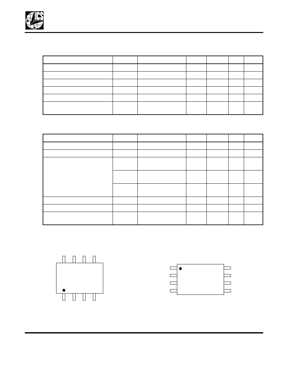
Marking Diagrams
(Marking for lead (Pb) free device shown below)
Parameter
Symbol
Conditions
Min.
Typ.
Max.
Units
Input/Output Clock Frequency
80
167
MHz
Input Clock Duty Cycle
Time above VDD/2
20
80
%
Output Clock Duty Cycle
Time above 1.5 V
40
50
60
%
Output Clock Rise Time
t
OR
0.8 to 2.0V
1.5
ns
Output Clock Fall Time
t
OF
2.0 to 0.8V
1.5
ns
EMI Peak Frequency Reduction
3rd - 19th odd
harmonics
7 to 14
dB
Parameter
Symbol
Conditions
Min.
Typ.
Max.
Units
Input/Output Clock Frequency
25
165
MHz
Input Clock Duty Cycle
Time above VDD/2
20
80
%
Output Clock Duty Cycle
Time above 1.5 V,
40 MHz - 100 MHz
40
50
55
%
Time above 1.5 V,
100 MHz - 150 MHz
45
%
Time above 1.5 V,
>150 MHz
35
%
Output Clock Rise Time
t
OR
0.8 to 2.0V
1.5
ns
Output Clock Fall Time
t
OF
2.0 to 0.8V
1.5
ns
EMI Peak Frequency Reduction
3rd - 19th odd
harmonics
7 to 14
dB
MK1709S
YYWW
######
1
4
5
8
1
4
5
8
MK1709AG
YYWWLF
######
Low EMI Clock Generator
MDS 1709 D
7
Revision 031204
Integrated Circuit Systems, Inc.
525 Race Street, San Jose, CA 95126
tel (408) 297-1201
www.icst.com
MK1709
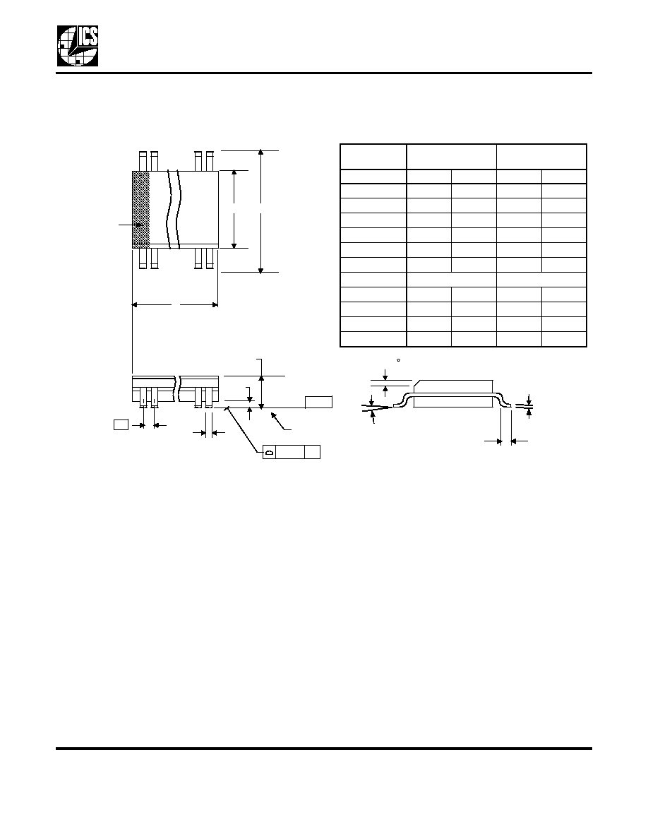
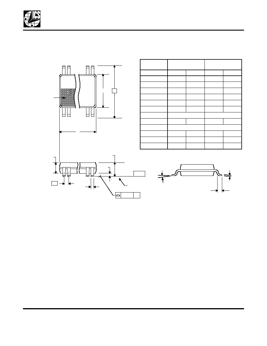
Package Outline and Package Dimensions
(8-pin SOIC, 150 Mil. Body)
Package dimensions are kept current with JEDEC Publication No. 95
INDEX
AREA
1 2
8
D
E
SEATING
PLANE
A1
A
e
- C -
B
.10 (.004)
C
C
L
H
h x 45
Millimeters
Inches
Symbol
Min
Max
Min
Max
A
1.35
1.75
.0532
.0688
A1
0.10
0.25
.0040
.0098
B
0.33
0.51
.013
.020
C
0.19
0.25
.0075
.0098
D
4.80
5.00
.1890
.1968
E
3.80
4.00
.1497
.1574
e
1.27 BASIC
0.050 BASIC
H
5.80
6.20
.2284
.2440
h
0.25
0.50
.010
.020
L
0.40
1.27
.016
.050
0
∞
8
∞
0
∞
8
∞
Low EMI Clock Generator
MDS 1709 D
8
Revision 031204
Integrated Circuit Systems, Inc.
525 Race Street, San Jose, CA 95126
tel (408) 297-1201
www.icst.com
MK1709
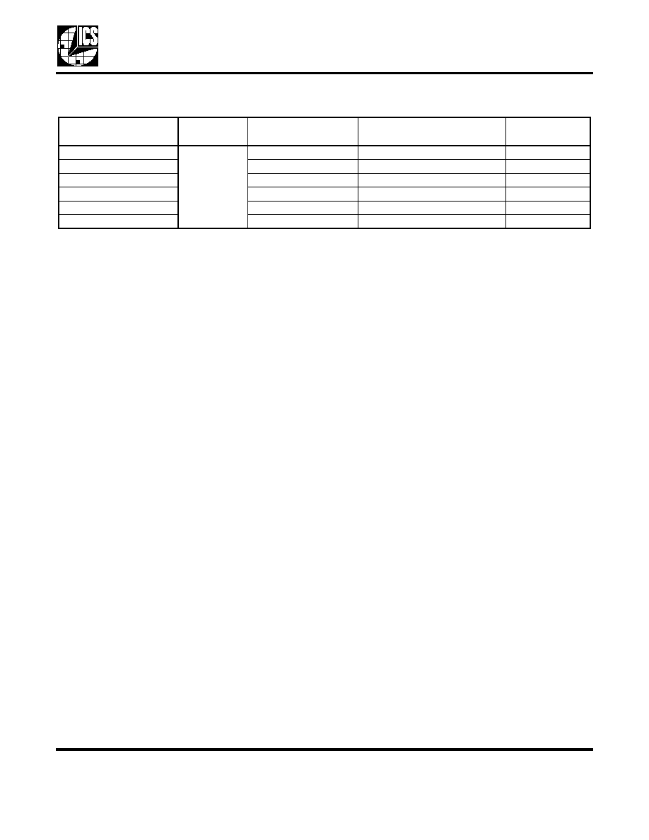
Package Outline and Package Dimensions
(8-pin TSSOP, 173 Mil. Body)
Package dimensions are kept current with JEDEC Publication No. 95
IN D E X
A R E A
1 2
8
D
E 1
E
S E A T IN G
P LA N E
A
1
A
A
2
e
- C -
b
a a a
C
c
L
Millimeters
Inches
Symbol
Min
Max
Min
Max
A
--
1.20
--
0.047
A1
0.05
0.15
0.002
0.006
A2
0.80
1.05
0.032
0.041
b
0.19
0.30
0.007
0.012
C
0.09
0.20
0.0035
0.008
D
3.90
3.10
0.114
0.122
E
6.40 BASIC
0.252 BASIC
E1
4.30
4.50
0.169
0.177
e
0.65 Basic
0.0256 Basic
L
0.45
0.75
0.018
0.030
0
∞
8
∞
0
∞
8
∞
aaa
-
0.10
-
0.004
Low EMI Clock Generator
MDS 1709 D
9
Revision 031204
Integrated Circuit Systems, Inc.
525 Race Street, San Jose, CA 95126
tel (408) 297-1201
www.icst.com
MK1709
Ordering Information
While the information presented herein has been checked for both accuracy and reliability, Integrated Circuit Systems (ICS)
assumes no responsibility for either its use or for the infringement of any patents or other rights of third parties, which would
result from its use. No other circuits, patents, or licenses are implied. This product is intended for use in normal commercial
applications. Any other applications such as those requiring extended temperature range, high reliability, or other extraordinary
environmental requirements are not recommended without additional processing by ICS. ICS reserves the right to change any
circuitry or specifications without notice. ICS does not authorize or warrant any ICS product for use in life support devices or
critical medical instruments.
Part / Order Number
Marking
Shipping
packaging
Package
Temperature
MK1709S
(see page 6)
Tubes
8-pin SOIC
0 to +85
∞ C
MK1709STR
Tape and Reel
8-pin SOIC
0 to +85
∞ C
MK1709AG
Tubes
8-pin TSSOP
0 to +85
∞ C
MK1709AGTR
Tape and Reel
8-pin TSSOP
0 to +85
∞ C
MK1709AGLF
Tubes
8-pin TSSOP
0 to +85
∞ C
MK1709AGLFTR
Tape and Reel
8-pin TSSOP
0 to +85
∞ C