MK2049-34A
MDS 2049-34A A
1
Revision 032504
Integrated Circuit Systems, Inc. 525 Race Street, San Jose, CA 95126 tel (408) 297-1201 www.icst.com
3.3 Volt Communications Clock VCXO PLL
Description
The MK2049-34A is a VCXO Phased Locked Loop
(PLL) based clock synthesizer that accepts multiple
input frequencies. With an 8 kHz clock input as a
reference, the MK2049-34A generates T1, E1, T3, E3,
ISDN, xDSL, and other communications frequencies.
This allows for the generation of clocks
frequency-locked and phase-locked to an 8 kHz
backplane clock, simplifying clock synchronization in
communications systems. The MK2409-34 can also
accept a T1 or E1 input clock and provide the same
output for loop timing. All outputs are frequency locked
together and to the input.
This part also has a jitter-attenuated Buffer capability.
In this mode, the MK2049-34A is ideal for filtering jitter
from 27 MHz video clocks or other clocks with high
jitter.
ICS can customize these devices for many other
different frequencies.
Features
∑
Packaged in 20-pin SOIC
∑
3.3 V + 5% operation
∑
Fixed I/O phase relationship on all selections
∑
Meets the TR62411, ETS300 011, and GR-1244
specification for MTIE, Pull-in/Hold-in Range, Phase
Transients, and Jitter Generation for Stratum 3, 4,
and 4E
∑
Accepts multiple inputs: 8 kHz backplane clock, Loop
Timing frequencies, or 10 to 36 MHz
∑
Locks to 8 kHz + 100 ppm (External mode)
∑
Buffer Mode allows jitter attenuation of 10 to 36 MHz
input and x1/x0.5 or x2/x4 outputs
∑
Exact internal ratios enable zero ppm error
∑
Output clock rates include T1, E1, T3, E3, ISDN,
xDSL, and the OC3 submultiples
∑
See the MK2049-01, -02, and -03 for more selections
at 5 V
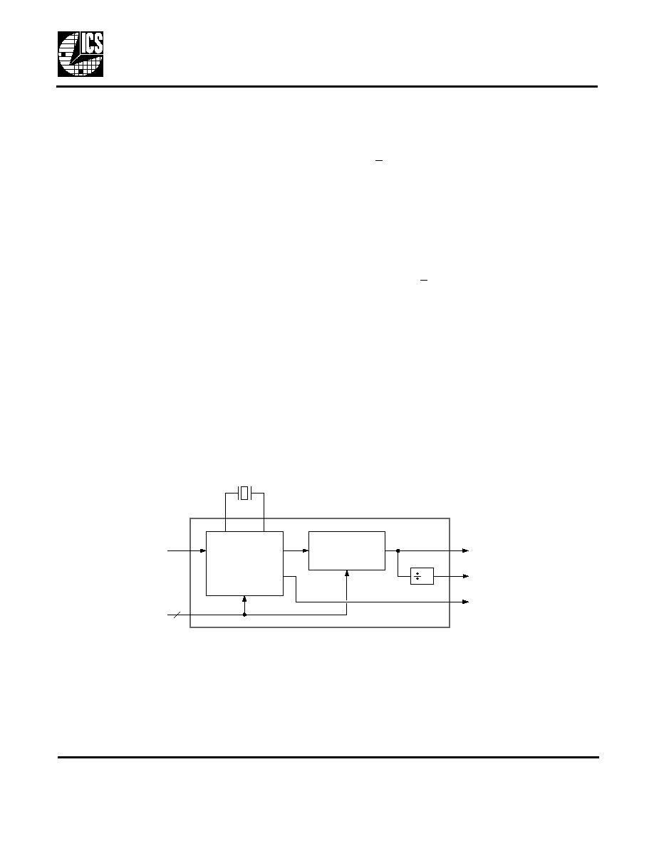
Block Diagram
VCXO-B
ASED
PLL
(M
ASTER
C
LOCK
G
ENERATOR
)
E
XTERNAL
P
ULLABLE
C
RYSTAL
(external loop filter)
F
REQUENCY
M
ULTIPLYING
PLL
2
I
NPUT
R
EFERENCE
C
LOCK
(T
YPICALLY
8
K
H
Z
)
C
LOCK
O
UTPUT
C
LOCK
O
UTPUT
/ 2
8
K
H
Z
(R
EGENERATED
)
4
F
REQUENCY
S
ELECT

3.3 Volt Communications Clock VCXO PLL
MDS 2049-34A A
2
Revision 032504
Integrated Circuit Systems, Inc. 525 Race Street, San Jose, CA 95126 tel (408) 297-1201 www.icst.com
MK2049-34A
Pin Assignment
20-pin (300) mil SOIC
Pin Descriptions
16
1
15
2
14
FS1
FS0
3
13
X2
4
12
X1
RES
5
11
VDD
6
CAP2
7
FCAP
8
VDD
GND
CAP1
VDD
GND
GND
CLK
ICLK
9
10
CLK/2
FS3
8k
FS2
20
19
18
17
Pin
Number
Pin
Name
Pin
Type
Pin Description
1
FS1
Input
Frequency select 1. Determines CLK input/outputs per table on page 3.
2
X2
XO
Crystal connection. Connect to a MHz crystal as shown in table on page 3.
3
X1
XI
Crystal connection. Connect to a MHz crystal as shown in table on page 3.
4
VDD
Power
Power supply. Connect to +3.3 V.
5
FCAP
-
Filter capacitor. Connect a 1000 pF ceramic capacitor to ground.
6
VDD
Power
Power supply. Connect to +3.3 V.
7
GND
Power
Connect to ground
8
CLK
Output
Clock output determined by status of FS3:0 per tables on page 3.
9
CLK/2
Output
Clock output determined by status of FS3:0 per tables page 3. Always 1/2 of
CLK.
10
8k
Output
Recovered 8 kHz clock output.
11
FS2
Input
Frequency select 2. Determines CLK input/outputs per tables on page 3.
12
FS3
Input
Frequency select 3. Determines CLK input/outputs per tables on page 3.
13
ICLK
Input
Input clock connection. Connect to 8 kHz backplane or MHz clock.
14
GND
Power
Connect to ground.
15
VDD
Power
Power Supply. Connect to +3.3 V.
16
CAP1
Loop
Filter
Connect the loop filter ceramic capacitors and resistor between this pin and
CAP2.
17
GND
Power
Connect to ground.
18
CAP2
Loop
Connect the loop filter ceramic capacitors and resistor between this pin and
19
RES
-
Connect a 10-200k
resistor to ground. Contact ICS at telecom@icst.com for
recommended value for your application.
20
FS0
Input
Frequency select 0. Determines CLK input/outputs per table on page 3.
3.3 Volt Communications Clock VCXO PLL
MDS 2049-34A A
3
Revision 032504
Integrated Circuit Systems, Inc. 525 Race Street, San Jose, CA 95126 tel (408) 297-1201 www.icst.com
MK2049-34A
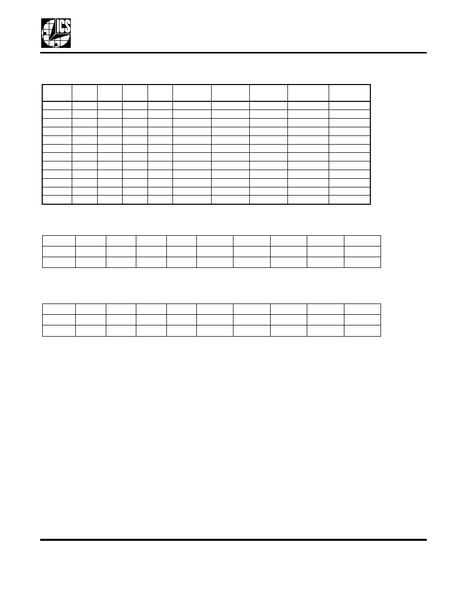
Output Decoding Table
- External Mode (MHz)
Output Decoding Table - Loop Timing Mode (MHz)
Output Decoding Table - Buffer Mode (MHz)
0 = connect directly to ground, 1 = connect directly to VDD
Crystal is connected to pins 2 and 3; clock input is applied to pin 13.
Operating Modes
The MK2049-34A has three operating modes: External, Loop Timing, and Buffer. Although each mode uses an
input clock to generate various output clocks, there are important differences in their input and crystal
requirements.
External Mode
The MK2049-34 accepts an external 8 kHz clock and will produce a number of common communication clock
frequencies. The 8 kHz input clock does not need to have a 50% duty cycle; a "high" or "on" pulse as narrow as 10
ns is acceptable. In the MK2049-34, the rising edges of CLK and CLK/2 are both aligned with the rising edge of the
8 kHz ICLK; refer to Figure 1 on page 4 for more details.
Loop Timing Mode
This mode can be used to remove the jitter from standard high-frequency communication clocks. For T1 and E1
inputs, the CLK/2 output will be the same as the input frequency, with CLK at twice the input frequency.
ICLK
FS3
FS2
FS1
FS0
CLK/2
CLK
8k
Crystal
Used (MHz)
N
8 kHz
0
0
0
0
1.544
3.088
8 kHz
12.352
1544
8 kHz
0
0
0
1
2.048
4.096
8 kHz
12.288
1536
8 kHz
0
0
1
0
22.368
44.736
8 kHz
11.184
1398
8 kHz
0
0
1
1
17.184
34.368
8 kHz
11.456
1432
8 kHz
0
1
0
0
19.44
38.88
8 kHz
9.72
1215
8 kHz
0
1
0
1
16.384
32.768
8 kHz
8.192
1024
8 kHz
0
1
1
0
17.664
35.328
8 kHz
17.664
2208
8 kHz
0
1
1
1
18.688
37.376
8 kHz
9.344
1168
8 kHz
1
0
1
0
7.68
15.36
8 kHz
15.36
1920
8 kHz
1
0
1
1
10.752
21.504
8 kHz
10.752
1344
8 kHz
1
1
0
0
10.24
20.48
8 kHz
10.24
1280
8 kHz
1
1
0
1
38.88
77.76
8 kHz
9.72
1215
ICLK
FS3
FS2
FS1
FS0
CLK/2
CLK
8k
Crystal
N
1.544
1
0
0
0
1.544
3.088
N/A
12.352
24
2.048
1
0
0
1
2.048
4.096
N/A
12.288
18
ICLK
FS3
FS2
FS1
FS0
CLK/2
CLK
8k
Crystal
N
19 - 36
1
1
1
0
ICLK/2
ICLK
N/A
ICLK/2
3
10 - 18
1
1
1
1
2*ICLK
4*ICLK
N/A
ICLK
3

3.3 Volt Communications Clock VCXO PLL
MDS 2049-34A A
4
Revision 032504
Integrated Circuit Systems, Inc. 525 Race Street, San Jose, CA 95126 tel (408) 297-1201 www.icst.com
MK2049-34A
Buffer Mode
Unlike the other two modes that accept only a single specified input frequency, Buffer Mode will accept a wider
range of input clocks. The input jitter is attenuated and the outputs on CLK and CLK/2 also provide the option of
getting x1, x2, x4, or 1/2 of the input frequency. For example, this mode can be used to remove the jitter from a 27
MHz clock, generating low-jitter 27 MHz and 13.5 MHz outputs.
Input and Output Synchronization
As shown in the tables on page 3, the MK2049-34A offers a Zero Delay feature in all selections. There is an internal
feedback path between ICLK and the output clocks, providing a fixed phase relationship between the input and
output, a requirement in many communication systems.
The rising edge of ICLK will be aligned with the rising edges of CLK and CLK/2 (8 kHz is used in this illustration, but
the same is true for the selections in the Loop Timing and Buffer Modes).
Measuring Zero Delay on the MK2049
The MK2049-34 produces low-jitter output clocks. In addition, this part has a very low bandwidth on the order of a
few Hertz. Since most 8 kHz input clocks will have high jitter, this can make measuring the input-to-output skew
(zero delay feature) very difficult. The MK2049 is designed to reject the input jitter; when the input and output clocks
are both displayed on an oscilloscope, they may appear not to be locked because the scope trigger point is
constantly changing with the input jitter. In fact, the input and output clocks probably are locked and the MK2049 will
have zero delay to the average position of the 8 kHz input clock. In order to see this clearly, a low jitter 8 kHz input
clock is necessary. Most lab frequency sources are NOT SUITABLE for this since they have high jitter at low
frequencies.
Frequency Locking to the Input
In all modes, the output clocks are frequency-locked to the input. The outputs will remain at the specified output
frequency as long as the combined variation of the input frequency and the crystal does not exceed 100 ppm. For
example, if the crystal can vary ±40 ppm (initial accuracy + temperature + aging), then the input frequency can vary
by up to 60 ppm and still have the output clock remain frequency-locked.
IC L K ( 8 k H z )
C L K ( M H z )
C L K /2 ( M H z )
F ig u r e 1 . M K 2 0 4 9 - 3 4 In p u t a n d O u t p u t C lo c k W a v e f o r m s

3.3 Volt Communications Clock VCXO PLL
MDS 2049-34A A
5
Revision 032504
Integrated Circuit Systems, Inc. 525 Race Street, San Jose, CA 95126 tel (408) 297-1201 www.icst.com
MK2049-34A
PC Board Layout
A proper board layout is critical to the successful use of the MK2049-34A. In particular, the CAP1 and CAP2 pins
are very sensitive to noise and leakage (CAP2 at pin 18 is the most sensitive). Traces must be as short as possible
and the two capacitors and resistor must be mounted next to the device as shown below. The capacitor shown
between pins 15 and 17, and the one between pins 4 and 7 are the power supply decoupling capacitors. The high
frequency output clocks on pins 8 and 9 should have a series termination of 33
connected close to the pin.
Additional improvements will come from keeping all components on the same side of the board, minimizing vias
through other signal layers, and routing other signals away from the MK2049. You may also refer to application note
MAN05 for additional suggestions on layout of the crystal selection.
The crystal traces should include pads for small capacitors from X1 and X2 to ground. These are used to adjust the
stray capacitance of the board to match the crystal load capacitance. The typical telecom reference frequency is
accurate to much less than 1 ppm, so the MK2049-34A may lock and run properly even if the board capacitance is
not adjusted with these fixed capacitors. However, ICS recommends that the adjustment capacitors be included to
minimize the effects of variation in individual crystals, temperature, and aging. The value of these capacitors
(typically 0 - 4 pF) is determined once for a given board layout, using the procedure found in application note
MAN05 (
http://www.icst.com/products/summary/man05.htm
).
16
1
15
2
14
3
13
4
12
5
11
6
7
8
9
10
20
19
18
17
G
G
cap
cap
resist
cap
ca
p
ca
p
resist
resist
resist
V
V
G
cap
cap
Optional -
see text
Cutout in ground and power plane.
Route all traces away from this area.
V
= connect to VDD
G
= connect to GND
Figure 2. Typical MK2049-34 Layout

3.3 Volt Communications Clock VCXO PLL
MDS 2049-34A A
6
Revision 032504
Integrated Circuit Systems, Inc. 525 Race Street, San Jose, CA 95126 tel (408) 297-1201 www.icst.com
MK2049-34A
External Component Selection
The MK2049-34A requires a minimum number of external components for proper operation. Decoupling capacitors
of 0.01
µ
F must be connected between VDD and GND pins close to the chip (especially pins 4 and 7, 15 and 17),
and 33
series terminating resistors should be used on clock outputs with traces longer than one inch (assuming
50
traces). The selection of additional external components is described in the following sections.
Loop Filter
Information on how to configure the external loop filter, connected between pins CAP1 and CAP2, can be found at
http://www.icst.com/products/telecom/telecom.htm
and
http://www.icst.com/PDF/MK2049-3x%20Addendum.pdf
.
Crystal Operation
The MK2049-34A operates by phase locking the input signal to a VCXO which consists of the recommended
pullable VCXO crystals and the integrated VCXO oscillator circuit on the MK2049-34A. To achieve the best
performance and reliability, the layout guidelines shown on the previous page should be closely followed.
The frequency of oscillation of a quartz crystal is determined by its cut and by the load capacitors connected to it.
The MK2049-34A has variable load capacitors on-chip which "pull" or change the frequency of the crystal. External
stray capacitance must be kept to a minimum to ensure maximum pullability of the crystal. To achieve this, the
layout should use short traces between the MK2049-34A and the crystal.
For the VCXO to operate correctly, a pullable crystal must be used. For more information, including a list of
approved crystals, please refer to application note MAN05 (http://www.icst.com/products/summary/man05.htm).
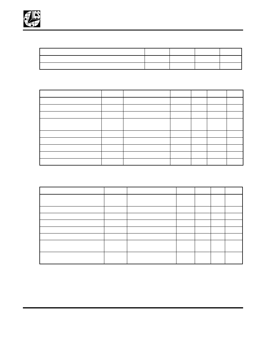
Absolute Maximum Ratings
Stresses above the ratings listed below can cause permanent damage to the MK2049-34A. These ratings,
which are standard values for ICS commercially rated parts, are stress ratings only. Functional operation of
the device at these or any other conditions above those indicated in the operational sections of the
specifications is not implied. Exposure to absolute maximum rating conditions for extended periods can
affect product reliability. Electrical parameters are guaranteed only over the recommended operating
temperature range.
Item
Rating
Supply Voltage, VDD
7 V
All Inputs and Outputs
-0.5 V to VDD+0.5 V
Ambient Operating Temperature
-40 to +85
∞
C
Storage Temperature
-65 to +150
∞
C
Junction Temperature
175
∞
C
Soldering Temperature
250
∞
C
3.3 Volt Communications Clock VCXO PLL
MDS 2049-34A A
7
Revision 032504
Integrated Circuit Systems, Inc. 525 Race Street, San Jose, CA 95126 tel (408) 297-1201 www.icst.com
MK2049-34A
Recommended Operation Conditions
DC Electrical Characteristics
Unless stated otherwise, VDD = 3.3 V ±5%, Ambient Temperature -40 to +85
∞
C
AC Electrical Characteristics
Unless stated otherwise, VDD = 3.3 V ±5%, Ambient Temperature -40 to +85
∞
C
Note 1: For loop timing modes and buffer modes, see tables on page 3 for required input clock frequencies
Parameter
Min.
Typ.
Max.
Units
Ambient Operating Temperature
-40
+85
∞
C
Power Supply Voltage (measured in respect to GND)
+3.15
+3.3
+3.45
V
Parameter
Symbol
Conditions
Min.
Typ.
Max.
Units
Operating Voltage
VDD
3.15
3.3
3.45
V
Input High Voltage
V
IH
2
V
Input Low Voltage
V
IL
0.8
V
Output High Voltage
(CMOS Level)
V
OH
I
OH
= -4 mA
VDD-0.4
V
Output High Voltage
V
OH
I
OH
= -8 mA
2.4
V
Output Low Voltage
V
OL
I
OL
= 8 mA
0.4
V
Operating Supply Current
I
DD
No Load, VDD=3.3 V
7
mA
Short Circuit Current
I
OS
Each Output
±50
mA
Input Capacitance
C
IN
FS3:0
5
pF
Parameter
Symbol
Conditions
Min.
Typ.
Max.
Units
Input Frequency
External Mode, Note 1
ICLK
8
kHz
Input Clock Pulse Width
t
pi
10
ns
Propagation Delay
ICLK to ICLK
0
6
ns
Output-Output Skew
CLK to CLK/2
150
ps
Output Clock Rise Time
t
OR
0.8 to 2.0 V
2
ns
Output Fall Time
t
OF
2.0 to 0.8 V
2
ns
Output Clock Duty Cycle, High
Time
at VDD/2, except 8 kHz
40
60
%
Actual mean frequency error
versus target
Any clock selection
0
0
ppm
3.3 Volt Communications Clock VCXO PLL
MDS 2049-34A A
8
Revision 032504
Integrated Circuit Systems, Inc. 525 Race Street, San Jose, CA 95126 tel (408) 297-1201 www.icst.com
MK2049-34A
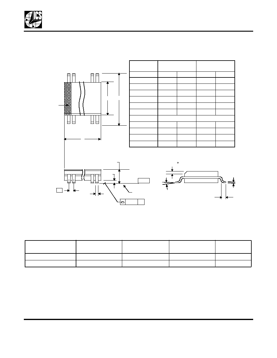
Package Outline and Package Dimensions
(20-pin SOIC, 300 Mil. Wide Body)
Package dimensions are kept current with JEDEC Publication No. 95
Ordering Information
While the information presented herein has been checked for both accuracy and reliability, Integrated Circuit Systems (ICS)
assumes no responsibility for either its use or for the infringement of any patents or other rights of third parties, which would
result from its use. No other circuits, patents, or licenses are implied. This product is intended for use in normal commercial
applications. Any other applications such as those requiring extended temperature range, high reliability, or other extraordinary
environmental requirements are not recommended without additional processing by ICS. ICS reserves the right to change any
circuitry or specifications without notice. ICS does not authorize or warrant any ICS product for use in life support devices or
critical medical instruments.
Part / Order Number
Marking
Shipping
packaging
Package
Temperature
MK2049-34SAI
MK2049-34SAI
Tubes
20-pin SOIC
-40 to +85
∞
C
MK2049-34SAITR
MK2049-34SAI
Tape and Reel
20-pin SOIC
-40 to +85
∞
C
INDEX
AREA
1 2
20
D
E
SEATING
PLANE
A1
A
e
- C -
B
.10 (.004)
C
C
L
H
h x 45
Millimeters
Inches
Symbol
Min
Max
Min
Max
A
--
2.65
--
.104
A1
0.10
--
.0040
--
B
0.33
0.51
.013
.020
C
0.18
0.32
.007
.013
D
12.60
13.00
.496
.512
E
7.40
7.60
.291
.299
e
1.27 BASIC
0.050 BASIC
H
10.00
10.65
.394
.419
h
0.25
0.75
.010
.029
L
0.40
1.27
.016
.050
0
∞
8
∞
0
∞
8
∞