 | –≠–ª–µ–∫—Ç—Ä–æ–Ω–Ω—ã–π –∫–æ–º–ø–æ–Ω–µ–Ω—Ç: MK2771-12 | –°–∫–∞—á–∞—Ç—å:  PDF PDF  ZIP ZIP |
MK2771-12
VCXO and Set-Top Clock Source
MDS 2771-12 A
1
Revision 061699
Printed 11/16/00
MicroClock Division of ICS ∑ 525 Race Street ∑ San Jose ∑ CA ∑ 95126∑(408)295-9800tel∑(408)295-9818fax
I C R O
C
LOC K
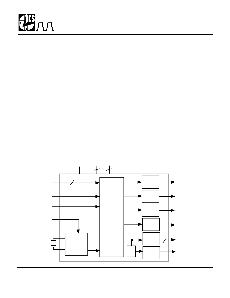
Block Diagram
Description
Features
The MK2771-12 is a low cost, low jitter, high
performance VCXO and clock synthesizer
designed for set-top boxes. The on-chip Voltage
Controlled Crystal Oscillator accepts a 0 to 3V
input voltage to cause the output clocks to vary by
±100 ppm. Using MicroClock's patented VCXO
and analog Phase-Locked Loop (PLL) techniques,
the device uses an inexpensive 13.5 MHz crystal
input to produce multiple output clocks including
a selectable processor clock, selectable UART and
audio clocks, a fixed 11.0592 MHz, and two low
skew copies of the 27 MHz. All clocks are
frequency locked to the 27.00 MHz output (and
to each other) with zero ppm error, so any output
can be used as the VCXO output.
This chip directly replaces the MK2771-02 when a
13.5 MHz input crystal is substituted for the
14.31818 MHz used on the -02. Additionally, the
-12 adds 24.576 MHz to the ACLK.
∑ Packaged in 20 pin SOIC
∑ Pin for pin and functional upgrade to MK2771-02
∑ Uses an inexpensive 13.5 MHz crystal
∑ On-chip patented
VCXO with pull range
of 200 ppm
∑ VCXO tuning voltage of 0 to 3 V
∑ Processor frequency of 16.67 MHz, 20 MHz,
32 MHz, 40 MHz, or 50 MHz
∑ Zero ppm synthesis error in all clocks (all exactly
track 27MHz VCXO) - patented
∑ 25 mA output drive capability at TTL levels
∑ Advanced, low power, sub-micron CMOS process
∑ 5 V operating voltage
Voltage
Controlled
Crystal
Oscillator
VDD
GND
Clock
Synthesis
Circuitry
Output
Buffer
Output
Buffer
27.000 MHz
Output
Buffers
3.6864 MHz
or 18.432 MHz
Processor Clock
Output
Buffer
49.152 MHz
or 24.576 MHz
3
2
2
PCS1:0
13.5 MHz
pullable
crystal
X1
X2
2
VIN
Output
Buffer
11.0592 MHz
AVDD
˜ 2
13.500 MHz
Output
Buffer
UCS
ACS
MK2771-12
VCXO and Set-Top Clock Source
MDS 2771-12 A
2
Revision 061699
Printed 11/16/00
MicroClock Division of ICS ∑ 525 Race Street ∑ San Jose ∑ CA ∑ 95126∑(408)295-9800tel∑(408)295-9818fax
I C R O
C
LOC K
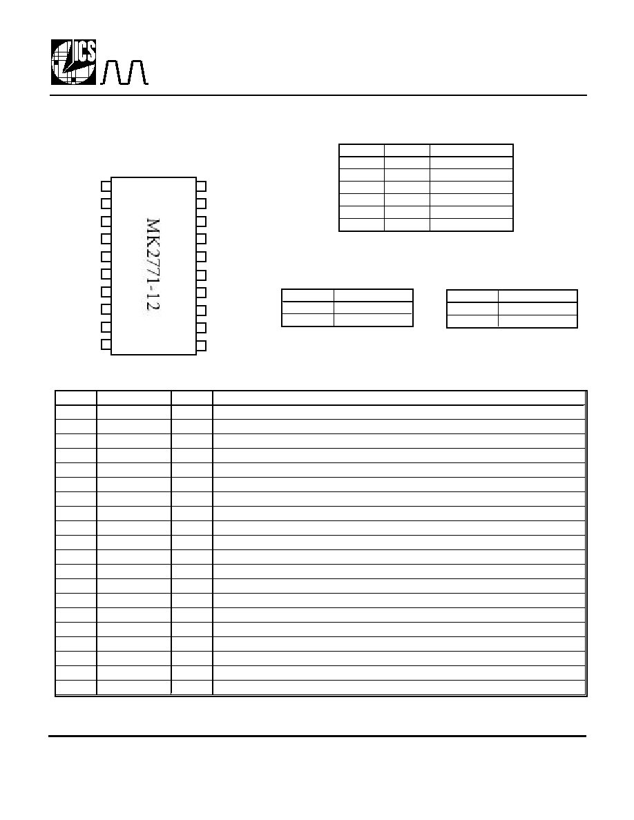
Pin Descriptions
Key: I = Input, TI = Tri-level input, O = output, P = power supply connection
Pin Assignment
Number
Name
Type
Description
1
PCS0
I
Processor Clock Select 0. Selects PCLK on pin 8. See table above.
2
X2
O
Crystal connection. Connect to a pullable 13.5 MHz crystal.
3
X1
I
Crystal connection. Connect to a pullable 13.5 MHz crystal.
4
AVDD
P
Analog VDD. Connect to +5V.
5
VIN
I
Voltage Input to VCXO. Zero to 3V signal which controls the frequency of the VCXO.
6
VDD
P
Connect to +5V.
7
GND
P
Connect to ground.
8
PCLK
O
Processor clock output determined by status of PCS1,0. See table above.
9
UCLK
O
UART clock output determined by status of UCS. See table above.
10
ACLK
O
49.152 MHz or 24.576 MHz clock output determined by ACS. See table above
11
13.5M
O
13.5 MHz clock output. Divide by two of the 27MHz VCXO output.
12
PCS1
TI
Processor Clock Select 1. Selects PCLK on pin 8. See table above.
13
11.06M
O
11.0592 MHz clock output.
14
GND
P
Connect to ground.
15
VDD
P
Connect to +5V.
16
27M
O
27.00 MHz VCXO clock output.
17
GND
P
Connect to ground.
18
27M
O
27.00 MHz VCXO clock output.
19
UCS
I
UART Clock Select. Selects UCLK on pin 9. See table above.
20
ACS
I
ACLK Select. Selects ACLK on pin 10. See table above.
1
16
2
3
4
15
14
13
AVDD
GND
X2
VDD
GND
5
6
7
8
12
11
10
9
ACLK
UCS
X1
PCS0
27M
ACS
27M
11.06M
13.5M
UCLK
PCLK
PCS1
PCS0
PCLK (MHz)
0
0
50.000
0
1
16.667
M
0
test
M
1
32.000
1
0
40.000
1
1
20.000
18
17
19
20
VIN
VDD
PCS1
GND
Processor Clock Select Table
UART Clock Table
UCS
UCLK (MHz)
0
18.432
1
3.6864
0 = connect directly to ground, 1 = connect directly
to VDD, M = leave floating or unconnected
ACLK Select Table
ACS
ACLK (MHz)
0
49.152
1
24.576
MK2771-12
VCXO and Set-Top Clock Source
MDS 2771-12 A
3
Revision 061699
Printed 11/16/00
MicroClock Division of ICS ∑ 525 Race Street ∑ San Jose ∑ CA ∑ 95126∑(408)295-9800tel∑(408)295-9818fax
I C R O
C
LOC K
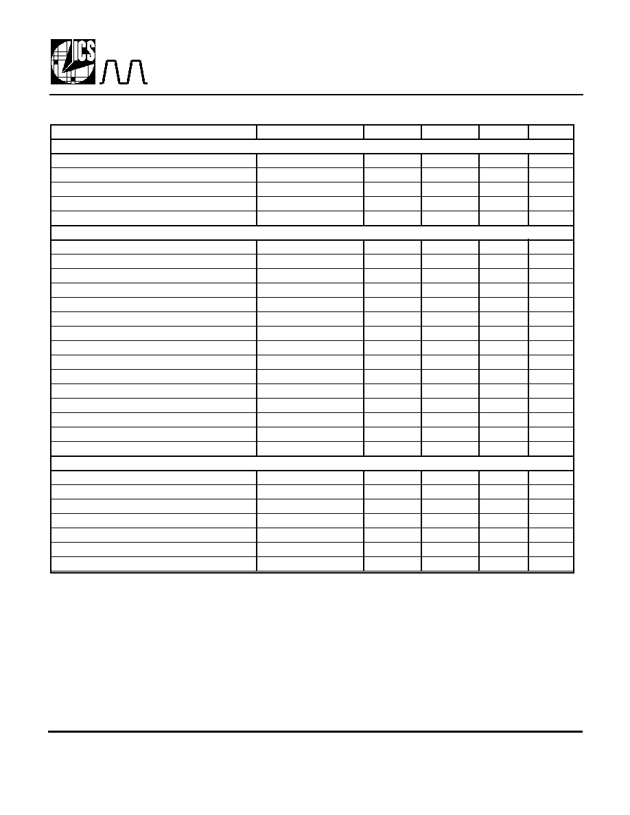
Parameter
Conditions
Minimum
Typical
Maximum
Units
ABSOLUTE MAXIMUM RATINGS (note 1)
ABSOLUTE MAXIMUM RATINGS (note 1)
Supply voltage, VDD
Referenced to GND
7
V
Inputs and Clock Outputs
Referenced to GND
-0.5
VDD+0.5
V
Ambient Operating Temperature
0
70
∞C
Soldering Temperature
Max of 10 seconds
260
∞C
Storage temperature
-65
150
∞C
DC CHARACTERISTICS (VDD = 5.0V unless noted)
DC CHARACTERISTICS (VDD = 5.0V unless noted)
Operating Voltage, VDD
4.75
5.25
V
Input High Voltage, VIH, X1 pin only
3.5
2.5
V
Input Low Voltage, VIL, X1 pin only
2.5
1.5
V
Input High Voltage, VIH (except PCS1)
2
V
Input Low Voltage, VIL (except PCS1)
0.8
V
Input High Voltage, VIH, PCS1 only
VDD-0.5
V
Input Low Voltage, VIL, PCS1 only
0.5
V
Output High Voltage, VOH
IOH=-25mA
2.4
V
Output Low Voltage, VOL
IOL=25mA
0.4
V
Output High Voltage, VOH, CMOS level
IOH=-8mA
VDD-0.4
V
Operating Supply Current, IDD
No Load, note 2
60
mA
Short Circuit Current
Each output
±100
mA
Input Capacitance
7
pF
Frequency synthesis error
All clocks
0
ppm
VIN, VCXO control voltage
0
3
V
AC CHARACTERISTICS (VDD = 5.0V unless noted)
AC CHARACTERISTICS (VDD = 5.0V unless noted)
Input Frequency
13.50000
MHz
Output Clock Rise Time
0.8 to 2.0V
1.5
ns
Output Clock Fall Time
2.0 to 0.8V
1.5
ns
Output Clock Duty Cycle
At 1.4V
40
60
%
Maximum Absolute Jitter, short term
200
ps
Skew of 27 MHz outputs
Rising edges at 1.4V
-500
0
500
ps
27 MHz output pullability, note 3
0V
VIN
3V
±100
ppm
Electrical Specifications
Notes:
1. Stresses beyond those listed under Absolute Maximum Ratings could cause permanent damage to the device. Prolonged
exposure to levels above the operating limits but below the Absolute Maximums may affect device reliability.
2. With PCLK at 50 MHz.
3. With a pullable crystal that conforms to ICS' specifications.
External Components
The MK2771-12 requires a minimum number of external components for proper operation. Decoupling
capacitors of 0.01µF should be connected between each VDD and GND, and betweeen AVDD and GND,
as close to the MK2771-12 as possible. A series termination resistor of 33
may be used for each clock
output.The 13.5 MHz crystal must be connected as close to the chip as possible. The 13.5 MHz crystal
should be a parallel mode, pullable, with load capacitance of 16 pF. Consult MicroClock for recommended
suppliers. Only the crystal should be connected to X1 and X2; do not connect load capacitors to these pins.
MK2771-12
VCXO and Set-Top Clock Source
MDS 2771-12 A
4
Revision 061699
Printed 11/16/00
MicroClock Division of ICS ∑ 525 Race Street ∑ San Jose ∑ CA ∑ 95126∑(408)295-9800tel∑(408)295-9818fax
I C R O
C
LOC K
While the information presented herein has been checked for both accuracy and reliability, Integrated Circuit Systems, Inc. (ICS) assumes no responsibility for either its use or for
the infringement of any patents or other rights of third parties, which would result from its use. No other circuits, patents, or licenses are implied. This product is intended for use
in normal commercial applications. Any other applications such as those requiring extended temperature range, high reliability, or other extraordinary environmental
requirements are not recommended without additional processing by ICS. ICS reserves the right to change any circuitry or specifications without notice. ICS does not authorize
or warrant any ICS product for use in life support devices or critical medical instruments.
Package Outline and Package Dimensions
Ordering Information
Part/Order Number
Marking
Shipping packaging
Package
Temperature
MK2771-12S
MK2771-12S
tubes
20 pin SOIC
0-70∞C
MK2771-12STR
MK2771-12S
tape and reel
20 pin SOIC
0-70∞C
b
D
E
H
e
Q
c
h x 45∞
A
20 pin SOIC
Inches
Inches
Millimeters
Millimeters
Symbol
Min
Max
Min
Max
A
0.092
0.104
2.3368
2.6416
b
0.014
0.019
0.356
0.483
c
0.009
0.012
0.229
0.305
D
0.490
0.512
12.446
13.005
E
0.290
0.300
7.366
7.620
H
0.394
0.419
10.008
10.643
e .050 BSC
.050 BSC
1.27 BSC
1.27 BSC
h
0.016
0.406
L
0.016
0.035
0.406
0.889
Q
0.003
0.011
0.076
0.279
L