AUGUST 2000
DSC-5285/03
1
©2000 Integrated Device Technology, Inc.
9Mb Pipelined
QDRTM SRAM
Burst of 2
QDR SRAMs and Quad Data Rate comprise a new family of products developed by Cypress Semiconductor, IDT, Inc. and Micron Technology.
Advance
Information
IDT71T62805
Features
x
x
x
x
x
9Mb Density (512Kx18)
x
x
x
x
x
Separate Independent Read and Write Data Ports
-- Supports concurrent transactions
x
x
x
x
x
333MHz Data Rate for High Bandwidth Applications
x
x
x
x
x
Fast Clock-to ValidDR access times
-- 2.5ns for 166MHz version
x
x
x
x
x
Double Data Rate (DDR) interfaces on both Read and Write
ports (data transfered at 333MHz)
x
x
x
x
x
Two Input clocks (K and
K), using rising edges only, for
precise timing
x
x
x
x
x
Two output register clocks (C and
C) compensate for clock
skew and flight time mismatches
-- Clock and data delivered together to receiving device
x
x
x
x
x
Single multiplexed address input bus latches address
inputs for both READ and WRITE ports
x
x
x
x
x
Data forwarding feature provides most current data
x
x
x
x
x
Separate Port Selects for depth expansion
x
x
x
x
x
Internal synchronous self-timed three-state control
x
x
x
x
x
Synchronous internally self-timed writes
x
x
x
x
x
2.5V core power supply with HSTL Inputs and Outputs
x
x
x
x
x
165-ball,1.0mm pitch 13mm x 15mm fBGA Package
x
x
x
x
x
Variable drive HSTL output buffers
x
x
x
x
x
JTAG Interface
x
x
x
x
x
Variable Impedance HSTL.
Description
The IDT71T62805 is a 2.5V Synchronous pipelined SRAM equipped
with QDRTM architecture. QDR architecture consists of two separate
ports to access the memory array. The Read port has dedicated Data
Outputs to support Read operations, and the Write Port has dedicated
Data inputs to support Write operations. Access to each port is accom-
plished through a common address bus. The Read address is latched
on the rising edge of the K clock and the Write address is latched on the
rising edge of
K clock. QDR architecture has separate data inputs and
data outputs to completely eliminate the need to "turn-around" the data
bus required with common I/O devices. Accesses to the IDT71T62805
Read and Write ports are completely independent of one another. All
accesses are initiated synchronously on the rising edge of the positive
input clock (K). In order to maximize data throughout, both Read and
Write ports are equipped with Double Data Rate (DDR) interfaces. There-
fore, data can be transferred into the device on every rising edge of both
input clocks (K and
K) and out of the device on every rising edge of the
output clock (C and
C) thereby maximizing performance while simplifying
system design.
Depth expansion is accomplished with a Port Select input for each
port. Each Port Select allow each port to operate independently.
All synchronous inputs pass through input registers controlled by the
K or
K input clocks. All data outputs pass through output registers con-
trolled by the C or
C input clocks. Writes are conducted with on-chip
synchronous self-timed write circuitry.
A
0
- A
17
Address Inputs
Input
Synchronous
RPE
Read Port Enable
Input
Synchronous
WPE
Write Port Enable
Input
Synchronous
BW
0
,
BW
1
Individual Byte Write Selects
Input
Synchronous
K,
K
Clock signals for Data, Address and Control Inputs
Input
N/A
C,
C
Data Output Clocks
Input
N/A
D
0
-
D
17
Data Input
Input
Synchronous
Q
0
-
Q
17
Data Output
Output
Synchronous
ZQ
Output Impedance Matching Input
Input
Static
TMS, TDI, TCK
JTAG Inputs
Input
N/A
TDO
JTAG Output
Input
N/A
V
REF
Reference Voltage Input
Input
Static
V
DD,
V
DDQ
Core and Output Power
Supply
Static
V
SS
Ground
Supply
Static
5285 tbl 01
Pin Description Summary

6.42
2
IDT71T62805, 9 Mb (512K x 18-Bit) Pipelined SRAM with
Advance Information
QDRTM Architecture, Burst of 2 Commercial Temperature Range
Pin Definitions
Pin Descriptions continued on Page 3
.
Symbol
Pin Function
I/O
Active
Description
A
0
- A
17
Address Inputs
Input
N/A
Address inputs. Sampled on the rising edge of the K clock during active read and on the
rising edge of the
K
clock during active write operations. These address inputs are
multiplexed for both Read and Write ope rations. Internally, the device is organized 256Kx36
and delivered externally in two 18-bit words. Therefore, only 18 address inputs are needed
to acce ss the entire memory array. These inputs are ignored when appropriate port is
deselected. Therefore, on the rising edge of the postive input clock (K), these inputs are
ignored if the Read port is deselected. These inputs are ignored on the rising edge of the
negative input clock (
K
) when the Write port is deslected.
RPE
Read port
Enable
Input
Low
Read Port Enable. Sampled on the rising edge of positive input clock (K). When active, a
Read operation is initiated. Deasserting will cause the Read port to be deselected. When
deselected, the pending access is allowed to complete and the output drivers are
automatically three-stated following the next rising edge of the C clock. The IDT71T62805
organized internally as 256Kx36. Each read access consists of a burst of two sequential 18-
bit transfers over one clock cycle. The entire burst of two data words should be allowed to
complete. Initiating Read accesses on two consecutive K clock rises is a valid operation
resulting in two consecutive Read operations.
WPE
Write Port
Enable
Input
Low
Write Port Enable. Sampled on the rising edge of the K clock. When asserted active, a
write operation is initiated. Deasserting will deselect the Write port. When deselected, the
pending access is allowed to co mplete. The IDT71T62805 is organized internally as
256Kx18. Each write access consists of a burst of two sequential 18-bit transfers over one
clock cy cle. The entire burst of two data words should be allowed to complete. Initiating
Write accesses on two consecutive K clock rises is a valid operation resulting in two
consecutive Read Operations.
BW
0
,
BW
1
Individual Byte
Write Enables
Input
Low
Byte Write Enables 0 and 1. Sampled on the rising edge of the K and
K
clocks during write
operations. Used to selec t which byte is written into the device during the current portion of
the write operations. Bytes not writte n remain unaltered.
BW
0
controls D
[8:0]
while
BW
1
controls D
[17:9]
.
BW
0
and
BW
1
are sampled on same e dge as D[17:0]. Deselecting a Byte
Write Enable will cause the corresponding byte of data to be ignore d and not written into
the device.
K
Master Clock
Input
N/A
Positive Input Clock Input. The rising edge of K is used to capture synchronous inputs
(data, address and contro l) to the device and drive out data through Q[17:0} when in single
clock mode.
K
Master Clock
Input
N/A
Negative Input Clock Input.
K
is used to capture synchronous inputs (data, address and
control) being presented to the device and drive out data through Q[17:0] when in single
clock mode. All accesses are initiated on the rising edge of K.
C
Output Data
Clock
Input
N/A
Positive Output Clock Input. C is used in conjuction with
C
clock out the Read data from the
device. C and
C
can travel with the data to the receiving device. When used in this way C and
C
can be used to de-skew the flight times of various devices on the board (see application
example).
C
Output Data
Clock
Input
N/A
Negativ e Output Clock Input.
C
is used in conjunction with C to clo ck out the Read data
from the device. C and
C
c an travel with the data to the receiving devic e. When used in this
way C and
C
can be used to de-skew the flight times of various devic es on the board (see
application example).
D
0
- D
17
Data Input
Input
N/A
Data Input signals, sampled on the rising edge of K and
K
clocks during the data portion of
a valid write operation.
Q
0
- Q
17
Data Output
Output
N/A
Data Output signals. These pins drive out the requested data during a Read operation. Valid
data is driven out on the rising edge of both the C and
C
clocks during Read operations (or
K and
K
when in single clock mode). When the read is deselected, Q[17:0} are
automatically tri-stated.
ZQ
Programmable
Impedance
Matching
Input
N/A
Output Impedance Matching Input. This input is used to tune the device outputs to the
system data bus impedance
.
Q
[17:0]
output impedance are set to 0.2 x RQ, where RQ is a
resistor connected between ZQ and ground. Alternately, this pin can be connected to
directly to V
DD
, which enables the minimum impedance mod e. This pin cannot be
connected directly to Vss or left unconnected.
5285 tbl 02a
6.42
3
IDT71T62805, 9 Mb (512K x 18-Bit) Pipelined SRAM with
Advance Information
QDRTM Architecture, Burst of 2 Commercial Temperature Range
Pin Definitions continued
Symbol
Pin Function
I/O
Active
Description
TMS
Test Mode
Select
Input
N/A
Gives input command for TAP controller; sample d rising edge of TCK.
TDI
Test Data
Input
Input
N/A
Serial input of registers placed between TDI and TDO. Sampled o n rising edge of TCK.
TCK
Test Clock
Input
N/A
Clock input of TAP controller. Each TAP event is clocked. Test inputs are captured on rising
ed ge of TCK, while test outputs are driven from falling edge of TCK.
TDO
Test Data
Output
Output
N/A
Serial output of registers placed between TDI and TDO. This output is active dpending on
state of TAP controller.
V
REF
Input
Reference
Voltage
Input
N/A
Refe rence Voltage Input. Static input used to set the reference level for HSTL inputs,
no minally adjuste d to improve system noise margin.
V
DD
Core Power
Supply
N/A
N/A
Power supply inputs to the core of the device. Should b e connected to 2.5V power supply.
V
DDQ
I/O Power
Supply
N/A
N/A
Power supply inputs for the outputs of the device. Should be connected to 1.5V power
supply.
V
SS
Core Ground
N/A
N/A
Ground for the core of the device. Should be connected to ground of the system.
5285 tbl 02b
Introduction
Functional Overview
The IDT71T62805 is a synchronous pipelined Burst SRAM equipped
with both a Read Port and a Write Port. The Read port is dedicated to
Read operations and the Write Port is dedicated to Write operations. Data
flows into the SRAM through the Write port and out through the Read
Port. The IDT71T62805 multiplexes the address inputs in order to min-
imize the number of address pins required. The IDT71T62805 latches
the Read address on the rising edge of the positive input clock (K) and
latches the Write address on the rising edge of the negative input clock
(
K). By having separate Read and Write ports, the IDT71T62805 com-
pletely eliminates the need to "turn-around" the data bus and avoids any
possible data contention, thereby simplifying system design.
Accesses for both ports are initiated by the positive input clock (K). All
synchronous input timing is referenced from the rising edge of the input
clocks (K and
K) and all output timing is referenced to the output clocks, C
and
C (or K and K when in single clock mode.)
All synchronous data inputs (D
[17:0]
) inputs pass through input reg-
isters controlled by the input clocks (K and
K). All synchronous data
outputs (Q
[17:0]
) outputs pass through output registers controlled by the
rising edge of the output clocks (C and
C).
All synchronous control (
RPE, WPE, BW
0
,
BW
1
) inputs pass through
input registers controlled by the rising edge of the input clocks (K and
K).
Read Operations
Read operations are initiated by asserting
RPE active at the rising
edge of the positive input clock (K). The address presented to A
[17:0]
is
stored in the Read address register. Because the IDT71T62805 is a 36-
bit memory, it will access two 18-bit data words with each read operation.
Following the next K clock rise the data is available to be latched out of the
device, triggered by the C clock. On the following C clock rise the
corresponding lower order word of data is driven onto the Q
[17:0]
. On
the subsequent rising edge of
C the higher order data word is driven
onto the Q
[17:0]
. The requested data will be valid 2.5ns from the rising
edge of the output clock (C or
C, 166MHz device). With the separate
Input and Output ports and the internal logic determining when the device
should drive the data bus, the QDR architecture has eliminated the need
for an output enable input to control the state of the output drivers.
Read accesses can be initiated on every rising edge of the positive
input clock (K). Doing so will pipeline the data flow such that data is
transferred out of the device on every rising edge of the output clocks (C
and
C). The IDT71T62805 will deliver the most recent data for the
address location being accessed. This includes forwarding data when a
Read and Write transactions to the same address location are initiated on
the same clock rise.
When the read port is deselected, the IDT71T62805 will first complete
the pending read tansactions. Synchronous internal circuitry will auto-
matically three-state the outputs following the next rising edge of the
positive output clock (C). This will allow for a seamless transition between
devices without the insertion of wait states.
The IDT71T62805 is equipped with internal logic that synchronously
controls the state of the output drivers. The logic inside the device deter-
mines when the output drivers need to be active or inactive. This ad-
vanced logic eliminates the need for an asynchronous output enable (
OE)
since the device will automatically enable/disable the output drivers during
the proper cycles. The IDT71T62805 will automatically power-up in a
deselcted state with the outputs in a three state condition.
Write Operations
Write operations are initiated by asserting
WPE active at the rising
edge of the positive input clock (K). On the same clock rise (K) the data
presented to D
[17:0]
is stored into the lower 18-bit Write Data register
provided
BW
[1:0]
are both asserted active. On the subsequent rising
edge of the negative input clock (
K), the information presented to A
[17:0]
Introduction continued on Page 4.

6.42
4
IDT71T62805, 9 Mb (512K x 18-Bit) Pipelined SRAM with
Advance Information
QDRTM Architecture, Burst of 2 Commercial Temperature Range
Introduction
continued
is latched and stored in the Write Address Register and the information
presented to D
[17:0]
is also stored into the upper 18-bit Write Data Reg-
ister provided
BW
[1:0]
are both asserted active. The 36 bits of data are
then written into the memory array at the specified location.
Write accesses can be initiated on every rising edge of the positive clock.
Doing so will pipeline the data flow such that 18-bits of data can be transferred
into the device on every rising edge of the input clocks (K and
K).
Byte Write operations are supported by the IDT71T62805. A write
operation is initiated by enabling the write port using
WPE. The bytes that
are written are determined by
BW
0
and
BW
1
which are sampled with
each set of 18-bit data word. Asserting the appropriate Byte Write Enable
input during the data portion of a write will allow the data being presented
to be latched and written into the device. De-asserting the Byte Write
Enable input during the data portion of a write will allow the data stored in
the device for that byte to remain unaltered. This feature can be used to
simplify READ/MODIFY/WRITE operations to a Byte Write operation.
When deselected, the write port will ignore all inputs.
Single Clock Mode
The IDT71T62805 can be used with a single clock mode. In this
mode the device will recognize only the pair of input clocks (K and
K) that
control both the input and output registers. This operation is identical to
the operation if the device had zero skew between the K/
K and C/C
clocks. All timing parameters remain the same in this mode. To use this
mode of operation, the user must tie C and
C to V
DD
. During power-up,
the device will sense the single clock input and operating in either single
clock or double clock mode. The clock mode should not be changed
during device operation.
Concurrent Transactions
The Read and Write ports on the IDT71T62805 operate completely
independently of one another. Since each port latches the address inputs
on different clock edges, the user can Read or Write to any location,
regardless of the transaction on the other port. Should the Read and
Write ports access the same location on the rising edge of the positive
input clock, the information presented to the D
[17:0]
will be forwarded to
the Q
[17:0]
such that no latency is required to access valid data. Coher-
ency is conducted on cycle boundaries. Once the second word of data is
latched into the device, the write operation is considered completed. At
this point, any access to that address location will receive that data until
altered by a subsequent Write operation. Coherency is not maintained
for Write operations initiated in the cycle after a Read.
Depth Expansion
The IDT71T62805 has a Port Enable input for each port. This allows for
easy depth expansion. Both Port Enables are sampled on the rising edge of
the positive input clock only (K). Each port enable input can disable the
specified port. Disabling a port will not affect the other port. All pending transac-
tions (Read and Write) will be completed prior to the device being disabled.
Programmable Impedance
An external resistor, RQ, must be connected between the ZQ pin on
the SRAM and V
SS
to allow the SRAM to adjust its output driver imped-
ance. The value of RQ must be 5X the value of the intended line
impedance driven by the SRAM, The allowable range of RQ to guar-
antee impedance matching with a tolerance of +/-10% is
between 175
and 350
, with V
DDQ
=1.5V. The output impedance is
adjusted every 1024 cycles to adjust for drifts in supply voltage and
temperature.
6.42
5
IDT71T62805, 9 Mb (512K x 18-Bit) Pipelined SRAM with
Advance Information
QDRTM Architecture, Burst of 2 Commercial Temperature Range
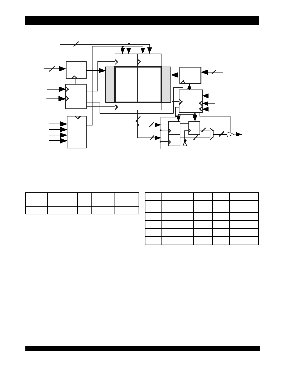
Functional Block Diagram
256Kx18
CLK
A
Gen.
K
K
Control
Logic
Address
Register
D
[17:0]
R
e
ad
A
d
d
.D
e
co
d
e
Read Data Reg.
RPE
WPE
Q
[17:0]
Control
Logic
Address
Register
Reg.
Reg.
Reg.
18
18
18
36
Write
18
BW
0
V
REF
W
ri
t
e
A
d
d
.
D
e
co
d
e
Data Reg
Write
Data Reg
Memory
Array
18
18
A
18
18
C
C
BW
1
256Kx18
Memory
Array
5285 drw 01
NOTE:
1. T
A
is the "instant on" case temperature.
Recommended Operating
Temperature and Supply Voltage
Recommended DC Operating
Conditions
NOTE:
1. -2.0V for pulse duration less than 20ns.
Grade
Ambient
Temperature
(1)
V
SS,
V
SSQ
V
DD
V
DDQ
Commercial
0∞C to +70∞C
OV
2.5 ± 100mV
1.4V to 1.9V
5285 tbl 03
Symbol
Parameter
Min.
Typ.
Max.
Unit
V
DD
Power Supply
Voltage
2.4
2.5
2.6
V
V
DDQ
I/O Supply Voltage
1.4
1.5
1.9
V
V
SS
Ground
0
0
0
V
V
IH
Input High Voltage
V
REF
+0.1
≠
V
DDQ
+0.3
V
V
IL
Input Low Voltage
≠0.3
(1)
≠
V
REF
≠0.1
V
5285 tbl 04