
1
IDT74FCT164245T
FAST CMOS 16-BIT BIDIRECTIONAL 3.3V TO 5V TRANSLATOR
INDUSTRIAL TEMPERATURE RANGE
AUGUST 1999
INDUSTRIAL TEMPERATURE RANGE
The IDT logo is a registered trademark of Integrated Device Technology, Inc.
© 1999 Integrated Device Technology, Inc.
DSC-2555/5
FEATURES:
∑ 0.5 MICRON CMOS Technology
∑ Bidirectional interface between 3.3V and 5V buses
∑ Control inputs can be driven from either 3.3V or 5V circuits
∑ ESD > 2000V per MIL-STD-883, Method 3015; > 200V using
machine model (C = 200pF, R = 0)
∑ V
CC1
= 5V
Ī
10%, V
CC2
= 2.7V to 3.6V
∑ High drive outputs (-32mA I
OH
, 64mA I
OL
) on 5V port
∑ Power off disable on both ports permits "live insertion"
∑ Typical V
OLP
(Output Ground Bounce) < 0.9V at V
CC1
= 5V,
V
CC2
= 3.3V, T
A
= 25įC
∑ Available in SSOP and TSSOP packages
FUNCTIONAL BLOCK DIAGRAM
IDT74FCT164245T
FAST CMOS 16-BIT
BIDIRECTIONAL
3.3V TO 5V TRANSLATOR
DESCRIPTION:
The FCT164245T 16-bit 3.3V-to-5V translator is built using advanced
dual metal CMOS technology. This high-speed, low-power transceiver is
designed to interface between a 3.3V bus and a 5V bus in a mixed 3.3V/
5V supply environment. This enables system designers to interface TTL
compatible 3.3V components with 5V components. The direction and output
enable controls operate these devices as either two independent 8-bit
transceivers or one 16-bit transceiver. The A port interfaces with the 3.3V
bus; the B port interfaces with the 5V bus. The direction control (xDIR) pin
controls the direction of data flow. The output enable pin (xOE) overrides
the direction control and disables both ports. These control signals can be
driven from either 3.3V or 5V devices.
The FCT164245T is ideally suited for driving high-capacitance loads
and low-impedance backplanes. The output buffers are designed with
power off disable capability to allow "hot insertion" of boards when used as
backplane drivers. They also allow interface between a mixed supply
system and external 5 volt peripherals.
1
DIR
1
OE
1
A
1
1
A
2
1
A
3
1
A
4
1
A
5
1
A
6
1
A
7
1
A
8
1
B
1
1
B
2
1
B
3
1
B
4
1
B
5
1
B
6
1
B
7
1
B
8
3
.
3
V
P
o
r
t
5
V
P
o
r
t
2
DIR
2
OE
2
A
1
2
A
2
2
A
3
2
A
4
2
A
5
2
A
6
2
A
7
2
A
8
2
B
1
2
B
2
2
B
3
2
B
4
2
B
5
2
B
6
2
B
7
2
B
8
3
.
3
V
P
o
r
t
5
V
P
o
r
t
1
47
48
2
3
5
6
46
44
43
41
40
38
37
8
9
11
12
2
4
36
35
33
32
30
25
29
27
26
22
23
13
14
16
17
19
20

2
INDUSTRIAL TEMPERATURE RANGE
IDT74FCT164245T
FAST CMOS 16-BIT BIDIRECTIONAL 3.3V TO 5V TRANSLATOR
PIN CONFIGURATION
Symbol
Description
Max
Unit
V
TERM
(2)
Terminal Voltage with Respect to GND
≠0.5 to +7
V
V
TERM
(3)
Terminal Voltage with Respect to GND
≠0.5 to Vcc
1
+0.5
V
T
A
Operating Temperature
≠40 to +85
įC
T
BIAS
Temperature Under Bias
≠55 to +125
įC
T
STG
Storage Temperature
≠55 to +125
įC
P
T
Power Dissipation
1
W
I
OUT
DC Output Current
≠60 to +120
mA
ABSOLUTE MAXIMUM RATINGS
(1)
(1)
(1)
(1)
(1)
NOTES:
1. Stresses greater than those listed under ABSOLUTE MAXIMUM RATINGS may cause
permanent damage to the device. This is a stress rating only and functional operation
of the device at these or any other conditions above those indicated in the operational
sections of this specification is not implied. Exposure to absolute maximum rating
conditions for extended periods may affect reliability.
2. All devices except Vcc
2
.
3. Power supply terminal Vcc
2
.
Symbol
Parameter
(1)
Conditions
Typ.
Max.
Unit
C
IN
Input Capacitance
V
IN
= 0V
3.5
6
pF
C
I/O
I/O Capacitance
V
OUT
= 0V
3.5
8
pF
CAPACITANCE
(T
A
= +25įC, F = 1.0MHz)
NOTE:
1. This parameter is measured at characterization but not tested.
PIN DESCRIPTION
Pin Names
Description
xOE
Output Enable Input (Active LOW)
xDIR
Direction Control Input
xAx
Side A Inputs or 3-State Outputs (3.3V Port)
xBx
Side B Inputs or 3-State Outputs (5V Port)
SSOP/ TSSOP
TOP VIEW
1
DIR
1
B
1
GND
1
B
3
V
CC1
GND
2
B
2
GND
V
CC1
GND
1
B
2
1
B
4
1
B
5
1
B
6
1
B
7
1
B
8
2
B
1
2
B
3
2
B
4
2
B
5
2
B
7
2
B
8
2
B
6
2
DIR
1
A
1
1
A
2
GND
1
A
3
1
A
4
V
CC2
1
A
5
1
A
6
1
A
7
1
A
8
2
A
1
2
A
2
2
A
3
2
A
4
V
CC2
2
A
5
2
A
7
2
A
8
2
A
6
GND
GND
GND
2
OE
1
OE
39
29
30
31
32
33
34
35
36
37
38
25
26
27
28
48
47
41
42
43
44
45
46
40
1
2
3
4
5
6
7
8
9
10
12
13
14
15
16
17
18
19
20
11
21
22
23
24
FUNCTION TABLE
(1)
Inputs
xOE
xDIR
Outputs
L
L
Bus B Data to Bus A
L
H
Bus A Data to Bus B
H
X
High Z State
NOTE:
1. H = HIGH Voltage Level
L = LOW Voltage Level
X = Don't Care
Z = High-Impedance
POWER SUPPLY SEQUENCING
In the 74FCT164245T, the condition of V
CC1
(V
CC2
≠ 0.5V) must be
maintained at all times. For the range of V
CC1
= (V
CC2
≠ 0.5V) to V
CC1
= (V
CC2
+ 0.9V), both the A and B ports will remain in a High-Impedance state.

3
IDT74FCT164245T
FAST CMOS 16-BIT BIDIRECTIONAL 3.3V TO 5V TRANSLATOR
INDUSTRIAL TEMPERATURE RANGE
Symbol
Parameter
Test Conditions
(1)
Min.
Typ.
(2)
Max.
Unit
V
IH
Input HIGH Level (Input and I/O pins)
Guaranteed Logic HIGH Level
2
--
5.5
V
V
IL
Input LOW Level (Input and I/O pins)
Guaranteed Logic LOW Level
≠0.5
--
0.8
V
I
IH
Input HIGH Current (Input pins)
V
CC1
= Max.
V
I
= 5.5V
--
--
Ī5
Input HIGH Current (I/O pins)
V
CC2
= Max.
V
I
= V
CC2
--
--
Ī15
ĶA
I
IL
Input LOW Current (Input pins)
V
I
= GND
--
--
Ī5
Input LOW Current (I/O pins)
V
I
= GND
--
--
Ī15
V
IK
Clamp Diode Voltage
V
CC2
= Min., I
IN
= ≠18mA
--
≠0.7
≠1.2
V
V
OH
Output HIGH Voltage
V
CC1
= V
CC2
= Min.
I
OH
= ≠0.1mA
V
CC2
≠0.2
--
--
V
V
IN
= V
IH
or V
IL
V
CC2
= 3V
I
OH
= ≠8mA
2.4
3
--
V
IN
= V
IH
or V
IL
V
OL
Output LOW Voltage
V
CC1
= Min.
I
OL
= 0.1mA
--
--
0.2
V
V
CC2
= Min.
I
OL
= 16mA
--
0.2
0.4
V
IN
= V
IH
or V
IL
I
OL
= 24mA
--
0.3
0.55
V
CC
= 3V
I
OL
= 24mA
--
0.3
0.5
V
IN
= V
IH
or V
IL
I
OFF
Input/Output Power Off Leakage
V
CC1
= 0V, V
CC2
= 0V, V
IN
or V
O
4.5V
--
--
Ī100
ĶA
I
OS
Short Circuit Current
(4)
V
CC1
= Max., V
CC2
= Max., V
O
= GND
(3)
≠70
≠105
≠150
mA
I
O
Output Drive Current
V
CC1
= Max., V
CC2
= Max., V
O
= 1.5V
(3)
≠40
≠60
≠90
mA
V
H
Input Hysteresis
--
--
150
--
mV
I
CC2
Quiescent Power Supply Current
V
CC1
= Max.
--
0.35
2
mA
I
CC2H
V
CC2
= Max.
I
CC2Z
V
IN
= GND or V
CC2
DC ELECTRICAL CHARACTERISTICS OVER OPERATING RANGE (A PORT, 3.3V)
Following Conditions Apply Unless Otherwise Specified:
V
CC1
= 5V Ī10%, V
CC2
= 2.7V to 3.6V, Industrial: T
A
= ≠40įC to +85įC
NOTES:
1. For conditions shown as Min. or Max., use appropriate value specified under Electrical Characteristics for the applicable device type.
2. Typical values are at V
CC1
= 5V, V
CC2
= 3.3V, +25įC ambient.
3. Not more than one output should be shorted at one time. Duration of the test should not exceed one second.
4. This parameter is guaranteed but not tested.
4
INDUSTRIAL TEMPERATURE RANGE
IDT74FCT164245T
FAST CMOS 16-BIT BIDIRECTIONAL 3.3V TO 5V TRANSLATOR
Symbol
Parameter
Test Conditions
(1)
Min.
Typ.
(2)
Max.
Unit
V
IH
Input HIGH Level (Input and I/O pins)
Guaranteed Logic HIGH Level
2
--
5.5
V
V
IL
Input LOW Level (Input and I/O pins)
Guaranteed Logic LOW Level
≠0.5
--
0.8
V
I
IH
Input HIGH Current (Input pins)
V
CC1
= Max.
V
I
= V
CC1
--
--
Ī5
Input HIGH Current (I/O pins)
V
CC2
= Max.
--
--
Ī15
ĶA
I
IL
Input LOW Current (Input pins)
V
I
= GND
--
--
Ī5
Input LOW Current (I/O pins)
--
--
Ī15
V
IK
Clamp Diode Voltage
V
CC1
= Min., I
IN
= ≠18mA
--
≠0.7
≠1.2
V
V
OH
Output HIGH Voltage
V
CC1
= Min.
I
OH
= ≠3mA
2.5
3.5
--
V
V
CC2
= Min.
I
OH
= ≠15mA
2.4
3.5
--
V
IN
= V
IH
or V
IL
I
OH
= ≠32mA
(5)
2
3
--
V
OL
Output LOW Voltage
V
CC1
= Min.
I
OL
= 64mA
--
0.2
0.55
V
V
CC2
= Min.
V
IN
= V
IH
or V
IL
I
OFF
Input/Output Power Off Leakage
V
CC1
= 0V, V
CC2
= 0V, V
IN
or V
O
4.5V
--
--
Ī100
ĶA
I
OS
Short Circuit Current
(4)
V
CC1
= Max., V
CC2
= Max., V
O
= GND
(3)
≠80
≠140
≠225
mA
I
O
Output Drive Current
V
CC1
= Max., V
CC2
= Max., V
O
= 2.5V
(3)
≠50
≠75
≠180
mA
V
H
Input Hysteresis
--
--
150
--
mV
I
CC2
Quiescent Power Supply Current
V
CC1
= Max.
--
0.08
1.5
mA
I
CC2H
V
CC2
= Max.
I
CC2Z
V
IN
= GND or V
CC2
DC ELECTRICAL CHARACTERISTICS OVER OPERATING RANGE (B PORT, 5V)
Following Conditions Apply Unless Otherwise Specified:
V
CC1
= 5V Ī10%, V
CC2
= 2.7V to 3.6V, Industrial: T
A
= ≠40įC to +85įC
NOTES:
1. For conditions shown as Min. or Max., use appropriate value specified under Electrical Characteristics for the applicable device type.
2. Typical values are at V
CC1
= 5V, V
CC2
= 3.3V, +25įC ambient.
3. Not more than one output should be shorted at one time. Duration of the test should not exceed one second.
4. This parameter is guaranteed but not tested.
5. Duration of the condition cannot exceed one second.

5
IDT74FCT164245T
FAST CMOS 16-BIT BIDIRECTIONAL 3.3V TO 5V TRANSLATOR
INDUSTRIAL TEMPERATURE RANGE
Symbol
Parameter
Test Conditions
(1)
Min.
Typ.
(2)
Max.
Unit
I
CC
Quiescent Power Supply Current
V
CC1
= Max., V
CC2
= Max.
--
12
30
ĶA
TTL Inputs HIGH
V
IN
= V
CC2
- 0.6V
(3)
I
CCD
Dynamic Power Supply
V
CC1
= Max., V
CC2
= Max.
V
IN
= V
CC2
--
75
120
ĶA/
Current
(4)
Outputs Open
V
IN
= GND
MHz
xOE = xDIR
= GND
One Input Togging
50% Duty Cycle
I
C
Total Power Supply Current
(6)
V
CC1
= Max., V
CC2
= Max.
V
IN
= V
CC2
- 0.6V
--
1.2
4.7
mA
Outputs Open
V
IN
= GND
f
I
= 10MHz
50% Duty Cycle
xOE = xDIR
= GND
One Bit Toggling
V
CC1
= Max., V
CC2
= Max.
V
IN
= V
CC2
- 0.6V
--
3.5
8.5
(5)
Outputs Open
V
IN
= GND
f
I
= 2.5MHz
50% Duty Cycle
xOE = xDIR
= GND
Sixteen Bits Toggling
POWER SUPPLY CHARACTERISTICS
NOTES:
1. For conditions shown as Min. or Max., use appropriate value specified under Electrical Characteristics for the applicable device type.
2. Typical values are at V
CC1
= 5V, V
CC2
= 3.3V, +25įC ambient.
3. Per TTL driven input. All other inputs at V
CC
or GND.
4. This parameter is not directly testable, but is derived for use in Total Power Supply Calculations.
5. Values for these conditions are examples of the I
CC
formula. These limits are guaranteed but not tested.
6. I
C
= I
QUIESCENT
+ I
INPUTS
+ I
DYNAMIC
I
C
= I
CC1
+ I
CC2
+ I
CC
D
H
N
T
+ I
CCD
(f
CP
N
CP
/2 + fiNi)
I
CC1
= Quiescent Current (I
CC1L
, I
CC1H
and I
CC1Z
)
I
CC2
= Quiescent Current (I
CC2L
, I
CC2H
and I
CC2Z
)
I
CC
= Power Supply Current for a TTL High Input
D
H
= Duty Cycle for TTL Inputs High
N
T
= Number of TTL Inputs at D
H
I
CCD
= Dynamic Current caused by an Input Transition Pair (HLH or LHL)
f
CP
= Clock Frequency for Register Devices (Zero for Non-Register Devices)
N
CP
= Number of Clock Inputs at f
CP
fi = Input Frequency
Ni = Number of Inputs at fi

6
INDUSTRIAL TEMPERATURE RANGE
IDT74FCT164245T
FAST CMOS 16-BIT BIDIRECTIONAL 3.3V TO 5V TRANSLATOR
Symbol
Parameter
Condition
(1)
Min.
(2)
Max.
Unit
t
PLH
Propagation Delay
C
L
= 50pF
1.5
5
ns
t
PHL
A to B
R
L
= 500
t
PLH
Propagation Delay
1.5
5
ns
t
PHL
B to A
t
PZH
Output Enable Time
1.5
6.5
ns
t
PZL
xOE to B
t
PHZ
Output Disable Time
1.5
6
ns
t
PLZ
xOE to B
t
PZH
Output Enable Time
1.5
6.5
ns
t
PZL
xOE to A
t
PHZ
Output Disable Time
1.5
6
ns
t
PLZ
xOE to A
t
PZH
Output Enable Time
1.5
6.5
ns
t
PZL
xDIR to B
(3)
t
PHZ
Output Disable Time
1.5
6
ns
t
PLZ
xDIR to B
(3)
t
PZH
Output Enable Time
1.5
6.5
ns
t
PZL
xDIR to A
(3)
t
PHZ
Output Disable Time
1.5
6
ns
t
PLZ
xDIR to A
(3)
SWITCHING CHARACTERISTICS OVER OPERATING RANGE
(1)
NOTES:
1. See test circuit and waveforms.
2. Minimum limits are guaranteed but not tested on Propagation Delays.
3. This parameter is guaranteed but not tested.

7
IDT74FCT164245T
FAST CMOS 16-BIT BIDIRECTIONAL 3.3V TO 5V TRANSLATOR
INDUSTRIAL TEMPERATURE RANGE
Pulse
Generator
R
T
D.U.T.
V
CC
V
IN
C
L
V
OUT
50pF
500
500
6V
Open
GND
3V
1.5V
0V
3V
1.5V
0V
3V
1.5V
0V
3V
1.5V
0V
DATA
INPUT
TIMING
INPUT
ASYNCHRONOUS CONTROL
PRESET
CLEAR
ETC.
SYNCHRONOUS CONTROL
t
SU
t
H
t
REM
t
SU
t
H
PRESET
CLEAR
CLOCK ENABLE
ETC.
HIGH-LOW-HIGH
PULSE
LOW-HIGH-LOW
PULSE
t
W
1.5V
1.5V
CONTROL
INPUT
3V
1.5V
0V
3V
0V
OUTPUT
NORMALLY
LOW
OUTPUT
NORMALLY
HIGH
SWITCH
6V
SWITCH
GND
V
OL
0.3V
0.3V
t
PLZ
t
PZL
t
PZH
t
PHZ
3V
0V
1.5V
1.5V
ENABLE
DISABLE
V
OH
SAME PHASE
INPUT TRANSITION
3V
1.5V
0V
1.5V
V
OH
t
PLH
OUTPUT
OPPOSITE PHASE
INPUT TRANSITION
3V
1.5V
0V
t
PLH
t
PHL
t
PHL
V
OL
TEST CIRCUITS AND WAVEFORMS
Propagation Delay
Test Circuits for All Outputs
Enable and Disable Times
Set-up, Hold, and Release Times
Pulse Width
Test
Switch
Open Drain
Disable Low
6V
Enable Low
Disable High
GND
Enable High
All Other Tests
Open
SWITCH POSITION
DEFINITIONS:
C
L
= Load capacitance: includes jig and probe capacitance.
R
T
= Termination resistance: should be equal to Z
OUT
of the Pulse Generator.
NOTES:
1. Diagram shown for input Control Enable-LOW and input Control Disable-HIGH.
2. Pulse Generator for All Pulses: Rate
1.0MHz; t
F
2.5ns; t
R
2.5ns.

8
INDUSTRIAL TEMPERATURE RANGE
IDT74FCT164245T
FAST CMOS 16-BIT BIDIRECTIONAL 3.3V TO 5V TRANSLATOR
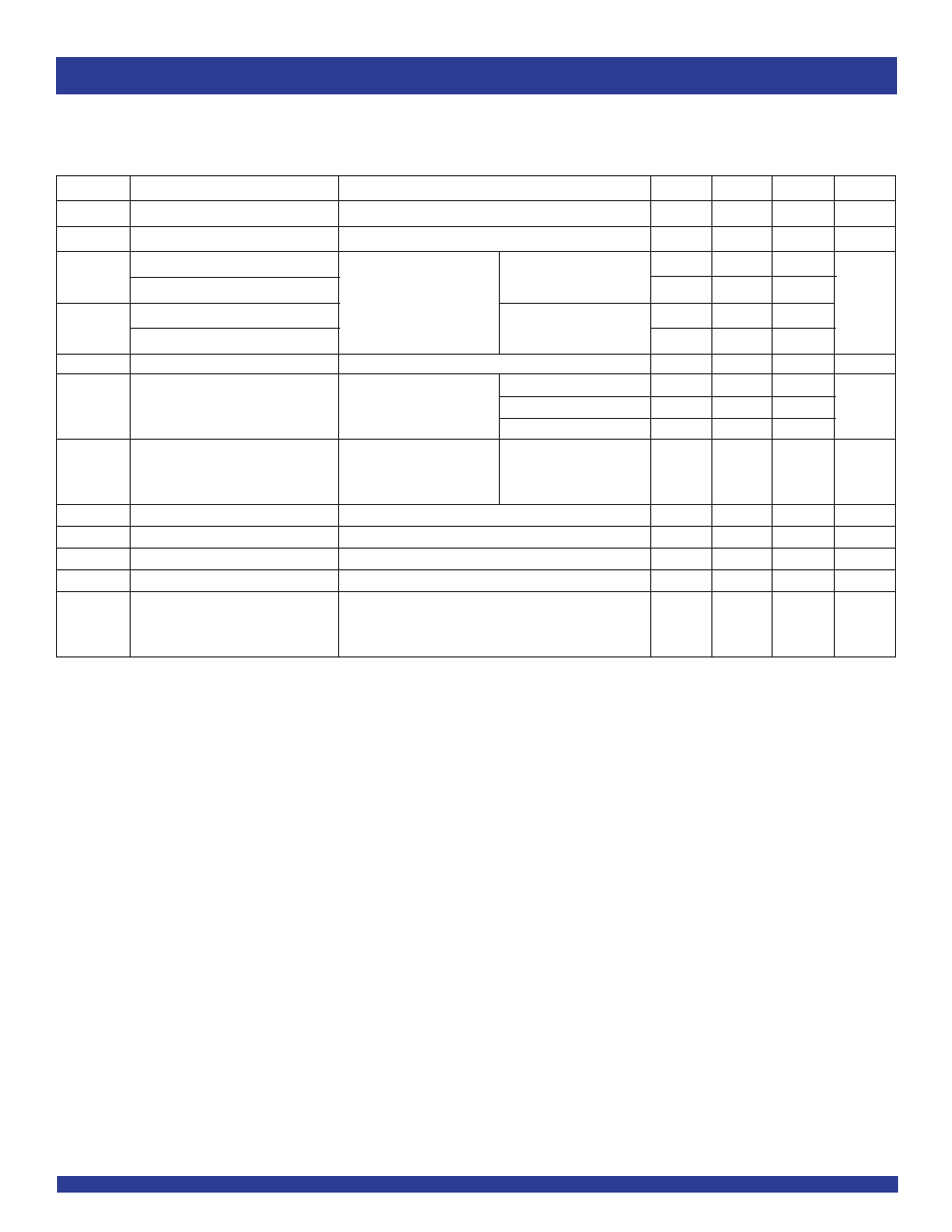
ORDERING INFORMATION
CORPORATE HEADQUARTERS
for SALES:
for Tech Support:
2975 Stender Way
800-345-7015 or 408-727-6116
logichelp@idt.com
Santa Clara, CA 95054
fax: 408-492-8674
(408) 654-6459
www.idt.com
IDT XX
Temp. Range
FCT
XX
Family
XXXX
Device Type
X
Package
PV
PA
245T
Shrink Small Outline Package
Thin Shrink Small Outline Package
16-Bit Bidirectional 3.3 Volt to 5 Volt Translator
74
≠40įC to +85įC
164
Double-Density