Äîêóìåíòàöèÿ è îïèñàíèÿ www.docs.chipfind.ru
INDUSTRIAL TEMPERATURE RANGE
IDT74LVC162244A
3.3V CMOS 16-BIT BUFFER/DRIVER WITH 3-STATE OUTPUTS
1
MARCH 1999
INDUSTRIAL TEMPERATURE RANGE
The IDT logo is a registered trademark of Integrated Device Technology, Inc.
© 1999 Integrated Device Technology, Inc.
DSC-4729/1
FEATURES:
· Typical t
SK(o)
(Output Skew) < 250ps
· ESD > 2000V per MIL-STD-883, Method 3015; > 200V using
machine model (C = 200pF, R = 0)
· V
CC
= 3.3V ± 0.3V, Normal Range
· V
CC
= 2.7V to 3.6V, Extended Range
· CMOS power levels (0.4
µµ
µµ
µ W typ. static)
· All inputs, outputs, and I/O are 5V tolerant
· Available in SSOP, TSSOP, and TVSOP packages
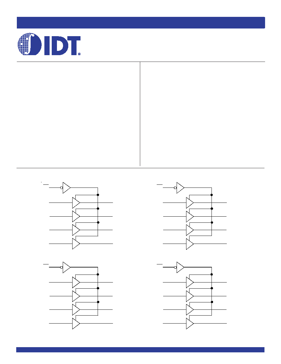
FUNCTIONAL BLOCK DIAGRAM
IDT74LVC162244A
APPLICATIONS:
· 5V and 3.3V mixed voltage systems
· Data communication and telecommunication systems
DRIVE FEATURES:
· Balanced Output Drivers: ±12mA
· Low switching noise
3.3V CMOS 16-BIT
BUFFER/DRIVER
WITH 3-STATE OUTPUTS
AND 5 VOLT TOLERANT I/O
DESCRIPTION:
The LVC162244A 16-bit buffer/driver is built using advanced dual metal
CMOS technology. The LVC162244A is designed specifically to improve
both the performance and density of 3-state memory address drivers, clock
drivers, and bus-oriented receivers and transmitters. The device can be
used as four 4-bit buffers, two 8-bit buffers, or one 16-bit buffer. This device
provides true outputs and symmetrical active-low output-enable (OE)
inputs.
All pins of this 16-bit buffer/driver can be driven from either 3.3V or 5V
devices. This feature allows the use of the device as a translator in a mixed
3.3V/5V supply system.
The LVC162244A has series resistors in the device output structure
which will significantly reduce line noise when used with light loads. This
driver has been developed to drive ±12mA at the designated threshold
levels.
1
A
1
1
A
2
1
A
3
1
A
4
1
Y
1
1
OE
1
Y
2
1
Y
3
1
Y
4
2
A
1
2
A
2
2
A
3
2
A
4
2
Y
1
2
OE
2
Y
2
2
Y
3
2
Y
4
3
A
1
3
A
2
3
A
3
3
A
4
3
Y
1
3
OE
3
Y
2
3
Y
3
3
Y
4
4
A
1
4
A
2
4
A
3
4
A
4
4
Y
1
4
OE
4
Y
2
4
Y
3
4
Y
4
1
47
46
44
43
48
41
40
38
37
25
36
35
33
32
24
30
29
27
26
13
14
16
17
19
20
22
23
2
3
5
6
8
9
11
12
INDUSTRIAL TEMPERATURE RANGE
2
IDT74LVC162244A
3.3V CMOS 16-BIT BUFFER/DRIVER WITH 3-STATE OUTPUTS
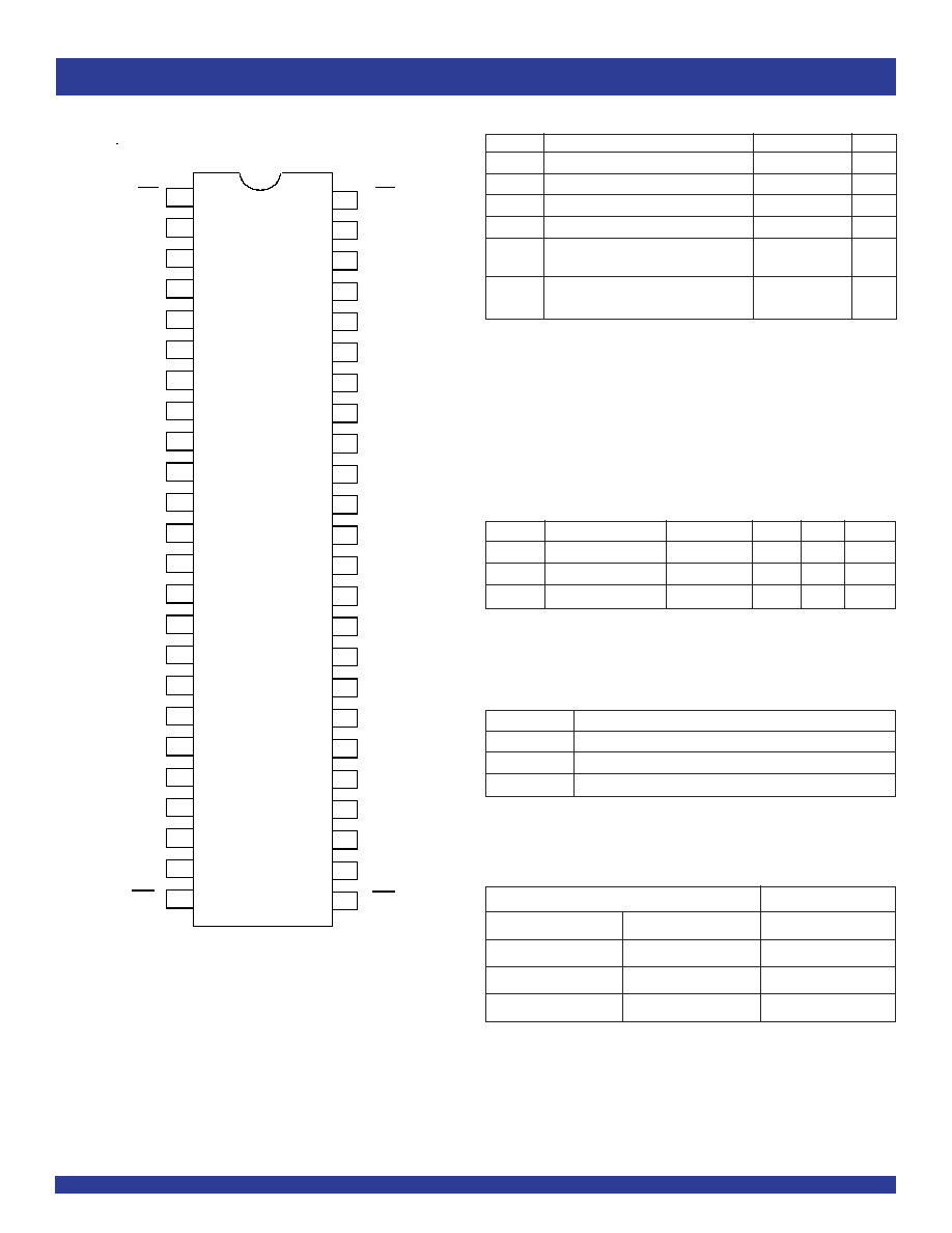
SSOP/ TSSOP/ TVSOP
TOP VIEW
PIN CONFIGURATION
NOTE:
1. H = HIGH Voltage Level
X = Don't Care
L = LOW Voltage Level
Z = High-Impedance
Inputs
Outputs
xOE
xAx
xYx
L
H
H
L
L
L
H
X
Z
FUNCTION TABLE
(EACH 4-BIT BUFFER)
(1)
Pin Names
Description
xOE
3-State Output Enable Inputs (Active LOW)
xAx
Data Inputs
xYx
3-State Outputs
PIN DESCRIPTION
NOTE:
1. As applicable to the device type.
Symbol
Parameter
(1)
Conditions
Typ.
Max.
Unit
C
IN
Input Capacitance
V
IN
= 0V
4.5
6
pF
C
OUT
Output Capacitance
V
OUT
= 0V
6.5
8
pF
C
I/O
I/O Port Capacitance
V
IN
= 0V
6.5
8
pF
CAPACITANCE
(T
A
= +25°C, F = 1.0MHz)
Symbol
Description
Max
Unit
V
TERM
(2)
Terminal Voltage with Respect to GND
0.5 to +6.5
V
V
TERM
(3)
Terminal Voltage with Respect to GND
0.5 to +6.5
V
T
STG
Storage Temperature
65 to +150
°C
I
OUT
DC Output Current
50 to +50
mA
I
IK
Continuous Clamp Current,
50
mA
I
OK
V
I
< 0 or V
O
< 0
I
CC
Continuous Current through each
±100
mA
I
SS
V
CC
or GND
ABSOLUTE MAXIMUM RATINGS
(1)
NOTES:
1. Stresses greater than those listed under ABSOLUTE MAXIMUM RATINGS may cause
permanent damage to the device. This is a stress rating only and functional operation
of the device at these or any other conditions above those indicated in the operational
sections of this specification is not implied. Exposure to absolute maximum rating
conditions for extended periods may affect reliability.
2. V
CC
terminals.
3. All terminals except V
CC
.
1
OE
1
Y
1
1
Y
2
GND
1
Y
3
1
Y
4
V
CC
2
Y
1
2
Y
2
GND
2
Y
3
2
Y
4
3
Y
1
3
Y
2
3
Y
4
4
OE
GND
V
CC
4
Y
1
4
Y
2
GND
4
Y
3
2
3
4
5
6
7
8
9
10
11
12
13
14
15
16
17
18
19
20
21
22
23
24
39
38
37
36
35
34
33
32
31
30
29
28
27
26
25
40
41
42
43
44
45
46
47
48
1
2
OE
1
A
1
1
A
2
GND
1
A
3
1
A
4
V
CC
2
A
1
2
A
2
2
A
3
2
A
4
3
A
1
GND
3
A
3
3
A
4
4
A
1
4
A
2
GND
4
A
3
4
A
4
3
OE
3
Y
3
4
Y
4
V
CC
3
A
2
GND
INDUSTRIAL TEMPERATURE RANGE
IDT74LVC162244A
3.3V CMOS 16-BIT BUFFER/DRIVER WITH 3-STATE OUTPUTS
3
Symbol
Parameter
Test Conditions
Min.
Typ.
(1)
Max.
Unit
V
IH
Input HIGH Voltage Level
V
CC
= 2.3V to 2.7V
1.7
--
--
V
V
CC
= 2.7V to 3.6V
2
--
--
V
IL
Input LOW Voltage Level
V
CC
= 2.3V to 2.7V
--
--
0.7
V
V
CC
= 2.7V to 3.6V
--
--
0.8
I
IH
Input Leakage Current
V
CC
= 3.6V
V
I
= 0 to 5.5V
--
--
±5
µA
I
IL
I
OZH
High Impedance Output Current
V
CC
= 3.6V
V
O
= 0 to 5.5V
--
--
±10
µA
I
OZL
(3-State Output pins)
I
OFF
Input/Output Power Off Leakage
V
CC
= 0V, V
IN
or V
O
5.5V
--
--
±50
µA
V
IK
Clamp Diode Voltage
V
CC
= 2.3V, I
IN
= 18mA
--
0.7
1.2
V
V
H
Input Hysteresis
V
CC
= 3.3V
--
100
--
mV
I
CCL
Quiescent Power Supply Current
V
CC
= 3.6V
V
IN
= GND or V
CC
--
--
10
µA
I
CCH
I
CCZ
3.6
V
IN
5.5V
(2)
--
--
10
I
CC
Quiescent Power Supply Current
One input at V
CC
- 0.6V, other inputs at V
CC
or GND
--
--
500
µA
Variation
DC ELECTRICAL CHARACTERISTICS OVER OPERATING RANGE
Following Conditions Apply Unless Otherwise Specified:
Operating Condition: T
A
= 40°C to +85°C
NOTE:
1. V
IH
and V
IL
must be within the min. or max. range shown in the DC ELECTRICAL CHARACTERISTICS OVER OPERATING RANGE table for the appropriate V
CC
range.
T
A
= 40°C to + 85°C.
OUTPUT DRIVE CHARACTERISTICS
Symbol
Parameter
Test Conditions
(1)
Min.
Max.
Unit
V
OH
Output HIGH Voltage
V
CC
= 2.3V to 3.6V
I
OH
= 0.1mA
V
CC
0.2
--
V
V
CC
= 2.3V
I
OH
= 4mA
1.9
--
I
OH
= 6mA
1.7
--
V
CC
= 2.7V
I
OH
= 4mA
2.2
--
I
OH
= 8mA
2
--
V
CC
= 3V
I
OH
= 6mA
2.4
--
I
OH
= 12mA
2
--
V
OL
Output LOW Voltage
V
CC
= 2.3V to 3.6V
I
OL
= 0.1mA
--
0.2
V
V
CC
= 2.3V
I
OL
= 4mA
--
0.4
I
OL
= 6mA
--
0.55
V
CC
= 2.7V
I
OL
= 4mA
--
0.4
I
OL
= 8mA
--
0.6
V
CC
= 3V
I
OL
= 6mA
--
0.55
I
OL
= 12mA
--
0.8
NOTES:
1. Typical values are at V
CC
= 3.3V, +25°C ambient.
2. This applies in the disabled state only.
INDUSTRIAL TEMPERATURE RANGE
4
IDT74LVC162244A
3.3V CMOS 16-BIT BUFFER/DRIVER WITH 3-STATE OUTPUTS
OPERATING CHARACTERISTICS, T
A
= 25°C
Symbol
Parameter
Test Conditions
Typical
Unit
C
PD
Power Dissipation Capacitance per Buffer/Driver Outputs enabled
C
L
= 0pF, f = 10Mhz
35
pF
C
PD
Power Dissipation Capacitance per Buffer/Driver Outputs disabled
4
SWITCHING CHARACTERISTICS
(1)
V
CC
= 2.7V
V
CC
= 3.3V ± 0.3V
Symbol
Parameter
Min.
Max.
Min.
Max.
Unit
t
PLH
Propagation Delay
--
5.6
1.1
4.4
ns
t
PHL
xAx to xYx
t
PZH
Output Enable Time
--
6.9
1
5.5
ns
t
PZL
xOE to xYx
t
PHZ
Output Disable Time
--
6.8
1.8
6.3
ns
t
PLZ
xOE to xYx
t
SK
(o)
Output Skew
(2)
--
--
--
500
ps
NOTES:
1. See TEST CIRCUITS AND WAVEFORMS. T
A
= 40°C to + 85°C.
2. Skew between any two outputs of the same package and switching in the same direction.
INDUSTRIAL TEMPERATURE RANGE
IDT74LVC162244A
3.3V CMOS 16-BIT BUFFER/DRIVER WITH 3-STATE OUTPUTS
5
Open
V
LOAD
GND
V
CC
Pulse
Generator
D.U.T.
500
500
C
L
R
T
V
IN
V
OUT
(1, 2)
LVC Link
INPUT
V
IH
0V
V
OH
V
OL
t
PLH1
t
SK
(x)
OUTPUT 1
OUTPUT 2
t
PHL1
t
SK
(x)
t
PLH2
t
PHL2
V
T
V
T
V
OH
V
T
V
OL
t
SK
(x)
= t
PLH2
-
t
PLH1
or
t
PHL2
-
t
PHL1
LVC Link
SAME PHASE
INPUT TRANSITION
OPPOSITE PHASE
INPUT TRANSITION
0V
0V
V
OH
V
OL
t
PLH
t
PHL
t
PHL
t
PLH
OUTPUT
V
IH
V
T
V
T
V
IH
V
T
LVC Link
DATA
INPUT
0V
0V
0V
0V
t
REM
TIMING
INPUT
ASYNCHRONOUS
CONTROL
SYNCHRONOUS
CONTROL
t
SU
t
H
t
SU
t
H
V
IH
V
T
V
IH
V
T
V
IH
V
T
V
IH
V
T
LVC Link
LOW-HIGH-LOW
PULSE
HIGH-LOW-HIGH
PULSE
V
T
t
W
V
T
LVC Link
CONTROL
INPUT
t
PLZ
0V
OUTPUT
NORMALLY
LOW
t
PZH
0V
SWITCH
CLOSED
OUTPUT
NORMALLY
HIGH
ENABLE
DISABLE
SWITCH
OPEN
t
PHZ
0V
V
OL+
V
LZ
V
OH
V
T
V
T
t
PZL
V
LOAD/2
V
LOAD/2
V
IH
V
T
V
OL
V
OH-
V
HZ
LVC Link
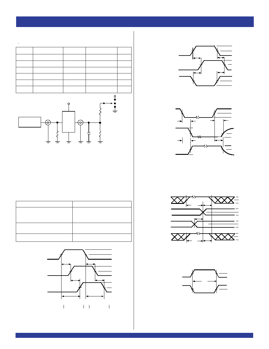
TEST CIRCUITS AND WAVEFORMS
Propagation Delay
Test Circuit for All Outputs
Enable and Disable Times
Set-up, Hold, and Release Times
NOTES:
1. For t
SK
(o) OUTPUT1 and OUTPUT2 are any two outputs.
2. For t
SK
(b) OUTPUT1 and OUTPUT2 are in the same bank.
DEFINITIONS:
C
L
= Load capacitance: includes jig and probe capacitance.
R
T
= Termination resistance: should be equal to Z
OUT
of the Pulse Generator.
NOTES:
1. Pulse Generator for All Pulses: Rate
10MHz; t
F
2.5ns; t
R
2.5ns.
2. Pulse Generator for All Pulses: Rate
10MHz; t
F
2ns; t
R
2ns.
Output Skew - t
SK
(
X
)
Pulse Width
NOTE:
1. Diagram shown for input Control Enable-LOW and input Control Disable-HIGH.
Symbol V
CC(1)
= 3.3V±0.3V V
CC(1)
= 2.7V
V
CC(2)
= 2.5V±0.2V
Unit
V
LOAD
6
6
2 x Vcc
V
V
IH
2.7
2.7
Vcc
V
V
T
1.5
1.5
Vcc
/ 2
V
V
LZ
300
300
150
mV
V
HZ
300
300
150
mV
C
L
50
50
30
pF
TEST CONDITIONS
SWITCH POSITION
Test
Switch
Open Drain
Disable Low
V
LOAD
Enable Low
Disable High
GND
Enable High
All Other Tests
Open