
INDUSTRIAL TEMPERATURE RANGE
IDT74LVCH32501A
3.3V CMOS 36-BIT REGISTERED TRANSCEIVER WITH 5V TOLERANT I/O
1
FEBRUARY 2000
INDUSTRIAL TEMPERATURE RANGE
The IDT logo is a registered trademark of Integrated Device Technology, Inc.
©2000 Integrated Device Technology, Inc.
DSC-4910/1
FEATURES:
∑ Typical t
SK(o)
(Output Skew) < 250ps
∑ ESD > 2000V per MIL-STD-883, Method 3015; > 200V using
machine model (C = 200pF, R = 0)
∑ V
CC
= 3.3V ± 0.3V, Normal Range
∑ V
CC
= 2.7V to 3.6V, Extended Range
∑ CMOS power levels (0.4
µµ
µµ
µ W typ. static)
∑ All inputs, outputs, and I/O are 5V tolerant
∑ Supports hot insertion
∑ Available in 114-ball LFBGA package
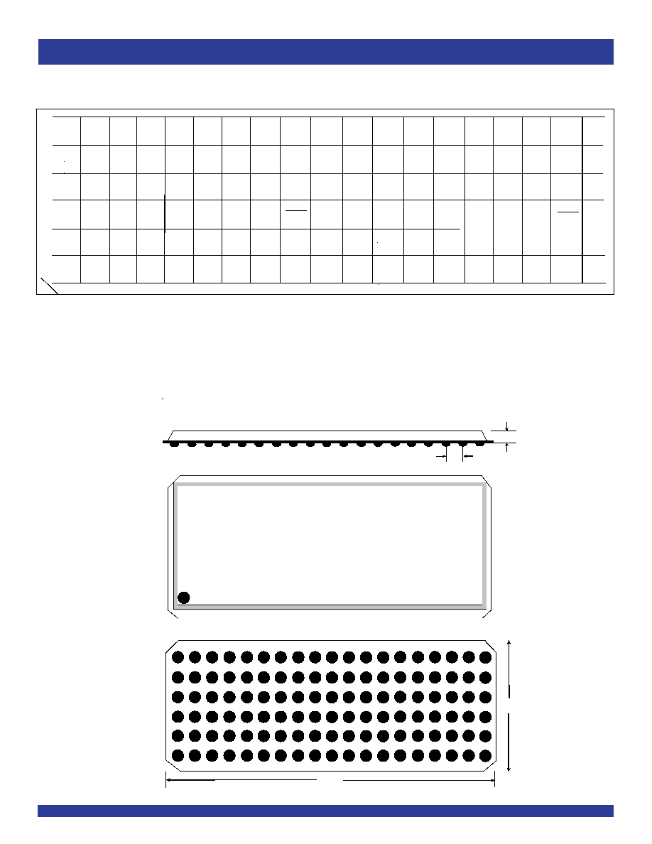
FUNCTIONAL BLOCK DIAGRAM
DRIVE FEATURES:
∑ High Output Drivers: ±24mA
∑ Reduced system switching noise
APPLICATIONS:
∑ 5V and 3.3V mixed voltage systems
∑ Data communication and telecommunication systems
IDT74LVCH32501A
DESCRIPTION:
This 36-bit registered transceiver is built using advanced dual metal
CMOS technology. This device combines D-type latches and D-type flip-
flops to allow data flow in transparent, latched, and clocked modes. Data flow
in each direction is controlled by output-enable (OEAB and OEBA), latch
enable (LEAB and LEBA), and clock (CLKAB and CLKBA) inputs. For A-
to-B data flow, the device operates in transparent mode when LEAB is
HIGH. When LEAB is LOW, the A data is latched if CLKAB is held at a HIGH
or LOW logic level. If LEAB is LOW, the A bus data is stored in the latch/flip-
flop on the LOW-to-HIGH transition of CLKAB. OEAB performs the output
enable function on the B port. Data flow from B port to A port is similar but
requires using OEBA, LEBA and CLKBA. Flow-through organization of
signal pins simplifies layout. All inputs are designed with hysteresis for
improved noise margin.
The LVCH32501A has been designed with a ±24mA output driver. This
driver is capable of driving a moderate to heavy load while maintaining
speed performance.
The LVCH32501A has "bus-hold" which retains the inputs' last state
whenever the input goes to a high impedance. This prevents floating inputs
and eliminates the need for pull-up/down resistors.
3.3V CMOS 36-BIT
REGISTERED TRANSCEIVER
WITH 5 VOLT TOLERANT I/O
AND BUS-HOLD
1
OEAB
1
CLKBA
1
LEBA
1
OEBA
1
CLKAB
1
LEAB
1
A
1
B3
J4
K3
J3
A4
A3
A2
TO 17 OTHER CHANNELS
C
D
C
D
C
D
C
D
1
B
1
A5
2
OEAB
2
CLKBA
2
LEBA
2
OEBA
2
CLKAB
2
LEAB
L3
V4
W3
V3
K5
K2
L2
L5
2
A
1
2
B
1
C
D
C
D
C
D
C
D
TO 17 OTHER CHANNELS
INDUSTRIAL TEMPERATURE RANGE
2
IDT74LVCH32501A
3.3V CMOS 36-BIT REGISTERED TRANSCEIVER WITH 5V TOLERANT I/O
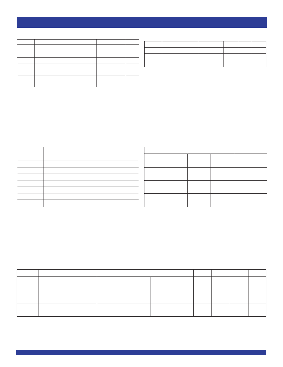
PIN CONFIGURATION
LFBGA
TOP VIEW
A
B
C
E
F
G
H
J
K
L
M
N
P
D
T
R
U
W
V
6
5
4
3
2
1
1
B
6
1
B
8
1
B
9
1
B
10
1
B
12
1
B
16
GND
1
B
4
1
B
5
1
B
7
1
B
14
1
B
15
1
B
11
1
B
13
1
B
2
1
B
3
1
B
1
V
CC
GND
2
B
6
1
B
17
2
B
7
2
B
9
2
B
8
2
B
3
2
B
10
1
B
18
2
B
12
GND
V
CC
1
A
1
GND
V
CC
2
OEAB
1
A
2
1
A
3
2
A
10
2
A
11
GND
V
CC
1
A
10
1
A
12
1
A
4
1
A
5
1
A
7
1
A
14
1
A
15
2
A
3
2
A
6
2
LEAB
2
A
1
2
A
8
1
A
18
1
A
6
1
A
8
1
A
9
1
A
16
1
A
11
1
A
13
2
A
2
2
A
4
1
A
17
2
A
5
2
A
7
GND
GND
V
CC
GND
V
CC
V
CC
GND
GND
1
LEBA
GND
GND
GND
2
B
5
2
B
4
1
LEAB
GND
1
CLKAB
1
CLKBA
2
B
11
2
B
13
2
B
14
GND
2
A
12
2
A
9
GND
V
CC
GND
1
OEAB
1
OEBA
2
A
13
2
A
14
2
A
18
2
A
16
2
OEBA
2
LEBA
2
B
16
2
B
15
2
B
18
2
B
17
GND
2
A
15
2
A
17
GND
2
CLKBA
2
CLKAB
2
B
1
2
B
2
GND
NC
NC
1.5mm Max.
1.4mm Nom.
1.3mm Min.
0.8mm
TOP VIEW
A B C D E F G H J K L M N P R T U V W
6
5
4
3
2
1
1
2
3
4
5
6
A B C D E F G H J K L M N P R T U V W
16mm
5.5mm
114 BALL LFBGA PACKAGE ATTRIBUTES
INDUSTRIAL TEMPERATURE RANGE
IDT74LVCH32501A
3.3V CMOS 36-BIT REGISTERED TRANSCEIVER WITH 5V TOLERANT I/O
3
Symbol
Description
Max
Unit
V
TERM
Terminal Voltage with Respect to GND
≠0.5 to +6.5
V
T
STG
Storage Temperature
≠65 to +150
∞C
I
OUT
DC Output Current
≠50 to +50
mA
I
IK
Continuous Clamp Current,
≠50
mA
I
OK
V
I
< 0 or V
O
< 0
I
CC
Continuous Current through each
±100
mA
I
SS
V
CC
or GND
ABSOLUTE MAXIMUM RATINGS
(1)
NOTE:
1. Stresses greater than those listed under ABSOLUTE MAXIMUM RATINGS may cause
permanent damage to the device. This is a stress rating only and functional operation
of the device at these or any other conditions above those indicated in the operational
sections of this specification is not implied. Exposure to absolute maximum rating
conditions for extended periods may affect reliability.
NOTE:
1. As applicable to the device type.
Symbol
Parameter
(1)
Conditions
Typ.
Max.
Unit
C
IN
Input Capacitance
V
IN
= 0V
4.5
6
pF
C
OUT
Output Capacitance
V
OUT
= 0V
6.5
8
pF
C
I/O
I/O Port Capacitance
V
IN
= 0V
6.5
8
pF
CAPACITANCE
(T
A
= +25∞C, F = 1.0MHz)
BUS-HOLD CHARACTERISTICS
Symbol
Parameter
(1)
Test Conditions
Min.
Typ.
(2)
Max.
Unit
I
BHH
Bus-Hold Input Sustain Current
V
CC
= 3V
V
I
= 2V
≠ 75
--
--
µA
I
BHL
V
I
= 0.8V
75
--
--
I
BHH
Bus-Hold Input Sustain Current
V
CC
= 2.3V
V
I
= 1.7V
--
--
--
µA
I
BHL
V
I
= 0.7V
--
--
--
I
BHHO
Bus-Hold Input Overdrive Current
V
CC
= 3.6V
V
I
= 0 to 3.6V
--
--
±500
µA
I
BHLO
NOTES:
1. Pins with Bus-Hold are identified in the pin description.
2. Typical values are at V
CC
= 3.3V, +25∞C ambient.
Pin Names
Description
OEAB
A-to-B Output Enable Input
OEBA
B-to-A Output Enable Input (Active LOW)
LEAB
A-to-B Latch Enable Input
LEBA
B-to-A Latch Enable Input
CLKAB
A-to-B Clock Input
CLKBA
B-to-A Clock Input
A x
A-to-B Data Inputs or B-to-A 3-State Outputs
(1)
B x
B-to-A Data Inputs or A-to-B 3-State Outputs
(1)
PIN DESCRIPTION
NOTE:
1. These pins have "Bus-Hold". All other pins are standard inputs, outputs, or I/Os.
FUNCTION TABLE
(1,2)
NOTES:
1. H = HIGH Voltage Level
L = LOW Voltage Level
X = Don't Care
Z = High Impedance
= LOW-to-HIGH Transition
2. A-to-B data flow is shown. B-to-A data flow is similar but uses OEBA, LEBA, and
CLKBA.
3. Output level before the indicated steady-state conditions were established.
4. Output level before the indicated steady-state conditions were established, provided
that CLKAB was HIGH before LEAB went LOW.
Inputs
Outputs
OEAB
LEAB
CLKAB
Ax
Bx
L
X
X
X
Z
H
H
X
L
L
H
H
X
H
H
H
L
L
L
H
L
H
H
H
L
L
X
B
(3)
H
L
H
X
B
(4)
INDUSTRIAL TEMPERATURE RANGE
4
IDT74LVCH32501A
3.3V CMOS 36-BIT REGISTERED TRANSCEIVER WITH 5V TOLERANT I/O
NOTE:
1. V
IH
and V
IL
must be within the min. or max. range shown in the DC ELECTRICAL CHARACTERISTICS OVER OPERATING RANGE table for the appropriate V
CC
range.
T
A
= ≠ 40∞C to + 85∞C.
OUTPUT DRIVE CHARACTERISTICS
Symbol
Parameter
Test Conditions
(1)
Min.
Max.
Unit
V
OH
Output HIGH Voltage
V
CC
= 2.3V to 3.6V
I
OH
= ≠ 0.1mA
V
CC
≠ 0.2
--
V
V
CC
= 2.3V
I
OH
= ≠ 6mA
2
--
V
CC
= 2.3V
I
OH
= ≠ 12mA
1.7
--
V
CC
= 2.7V
2.2
--
V
CC
= 3V
2.4
--
V
CC
= 3V
I
OH
= ≠ 24mA
2.2
--
V
OL
Output LOW Voltage
V
CC
= 2.3V to 3.6V
I
OL
= 0.1mA
--
0.2
V
V
CC
= 2.3V
I
OL
= 6mA
--
0.4
I
OL
= 12mA
--
0.7
V
CC
= 2.7V
I
OL
= 12mA
--
0.4
V
CC
= 3V
I
OL
= 24mA
--
0.55
Symbol
Parameter
Test Conditions
Min.
Typ.
(1)
Max.
Unit
V
IH
Input HIGH Voltage Level
V
CC
= 2.3V to 2.7V
1.7
--
--
V
V
CC
= 2.7V to 3.6V
2
--
--
V
IL
Input LOW Voltage Level
V
CC
= 2.3V to 2.7V
--
--
0.7
V
V
CC
= 2.7V to 3.6V
--
--
0.8
I
IH
Input Leakage Current
V
CC
= 3.6V
V
I
= 0 to 5.5V
--
--
±5
µA
I
IL
I
OZH
High Impedance Output Current
V
CC
= 3.6V
V
O
= 0 to 5.5V
--
--
±10
µA
I
OZL
(3-State Output pins)
I
OFF
Input/Output Power Off Leakage
V
CC
= 0V, V
IN
or V
O
5.5V
--
--
±50
µA
V
IK
Clamp Diode Voltage
V
CC
= 2.3V, I
IN
= ≠18mA
--
≠0.7
≠1.2
V
V
H
Input Hysteresis
V
CC
= 3.3V
--
100
--
mV
I
CCL
Quiescent Power Supply Current
V
CC
= 3.6V
V
IN
= GND or V
CC
--
--
10
µA
I
CCH
I
CCZ
3.6
V
IN
5.5V
(2)
--
--
10
I
CC
Quiescent Power Supply Current
One input at V
CC
- 0.6V, other inputs at V
CC
or GND
--
--
500
µA
Variation
DC ELECTRICAL CHARACTERISTICS OVER OPERATING RANGE
Following Conditions Apply Unless Otherwise Specified:
Operating Condition: T
A
= ≠40∞C to +85∞C
NOTES:
1. Typical values are at V
CC
= 3.3V, +25∞C ambient.
2. This applies in the disabled state only.
INDUSTRIAL TEMPERATURE RANGE
IDT74LVCH32501A
3.3V CMOS 36-BIT REGISTERED TRANSCEIVER WITH 5V TOLERANT I/O
5
OPERATING CHARACTERISTICS, V
CC
= 3.3V ± 0.3V, T
A
= 25∞C
Symbol
Parameter
Test Conditions
Typical
Unit
C
PD
Power Dissipation Capacitance per Transceiver Outputs enabled
C
L
= 0pF, f = 10Mhz
pF
C
PD
Power Dissipation Capacitance per Transceiver Outputs disabled
SWITCHING CHARACTERISTICS
(1)
V
CC
= 2.7V
V
CC
= 3.3V ± 0.3V
Symbol
Parameter
Min.
Max.
Min.
Max.
Unit
t
PLH
Propagation Delay
1.5
5.2
1.5
4.6
ns
t
PHL
Ax to Bx or Bx to Ax
t
PLH
Propagation Delay
1.5
6
1.5
5.3
ns
t
PHL
LEBA to Ax, LEAB to Bx
t
PLH
Propagation Delay
1.5
6
1.5
5.3
ns
t
PHL
CLKBA to Ax, CLKAB to Bx
t
PZH
Output Enable Time
1.5
6
1.5
5.6
ns
t
PZL
OEBA to Ax, OEAB to Bx
t
PHZ
Output Disable Time
1.5
6.5
1.5
5.8
ns
t
PLZ
OEBA to Ax, OEAB to Bx
t
SU
Set-up Time, HIGH or LOW
3
--
3
--
ns
Ax to CLKAB, Bx to CLKBA
t
H
Hold Time, HIGH or LOW
0
--
0
--
ns
Ax to CLKAB, Bx to CLKBA
t
SU
Set-up Time HIGH or LOW
Clock LOW
3
--
3
--
ns
Ax to LEAB,Bx to LEBA
ClockHIGH
2
--
2
--
t
H
Hold Time HIGH or LOW
1.5
--
1.5
--
ns
Ax to LEAB, Bx to LEBA
t
W
LEAB or LEBA Pulse Width HIGH
3
--
3
--
ns
t
W
CLKAB or CLKBA Pulse Width HIGH or LOW
3
--
3
--
ns
t
SK
(o)
Output Skew
(2)
--
--
--
500
ps
NOTES:
1. See TEST CIRCUITS AND WAVEFORMS. T
A
= ≠ 40∞C to + 85∞C.
2. Skew between any two outputs of the same package and switching in the same direction.