
1
The IDT logo is a registered trademark of Integrated Device Technology, Inc
INDUSTRIAL TEMPERATURE RANGE
2004 Integrated Device Technology, Inc.
JULY 19, 2004
DSC-6222/3
FUNCTIONAL BLOCK DIAGRAM
Filter and A/D
D/A and Filter
SLIC Signaling
CH1
VIN1
VOUT1
2 Inputs
2 I/Os
3 Outputs
CH2
CH3
CH4
DSP
Core
CH6
CH7
CH8
General
Control Logic
PLL and Clock
Generation
Serial Interface
PCM/GCI Interface
MPI
INT RESET
DR1/DD
DR2
DX1/DU
DX2
MCLK
CHCLK1
CHCLK2
CCLK
/TS
CS
CI/
DOUBLE
CO
FS
/FSC
BCLK
/DCL
TSX1 TSX2
Filter and A/D
D/A and Filter
SLIC Signaling
CH5
2 Inputs
2 I/Os
3 Outputs
VIN5
VOUT5
FEATURES
� 8 channel CODEC with on-chip digital filters
� Programmable A/�-law compressed or linear code conversion
� Meets ITU-T G.711 - G.714 requirements
� Programmable digital filters adapting to system requirements:
- AC impedance matching
- Transhybrid balance
- Frequency response correction
- Gain setting
� Supports two programmable PCM buses and one GCI bus
� Flexible PCM interface with up to 128 programmable time slots,
data rate from 512 kbit/s to 8.192 Mbit/s
� Broadcast mode for coefficient setting
� 7 SLIC signaling pins (including 2 debounced pins) per channel
� Fast hardware ring trip mechanism
� Two programmable tone generators per channel for testing,
ringing and DTMF generation
� 4 FSK generators shared by all 8 channels
� Two programmable chopper clocks
� Notch filters for 12 kHz and 16 kHz frequencies
� Master clock frequency selectable: 1.536 MHz, 1.544 MHz, 2.048
MHz, 3.072 MHz, 3.088 MHz, 4.096 MHz, 6.144 MHz, 6.176 MHz or
8.192 MHz
� Advanced test capabilities
- 5 analog loopback tests
- 6 digital loopback tests
- Level metering function
� High analog driving capability (300
AC)
� CODEC identification
� 3 V digital I/O with 5 V tolerance
� 3.3 V single power supply
� Operating temperature range: - 40�C to + 85�C
� Package available: 128 pin TQFP
OCTAL PROGRAMMABLE PCM CODEC
IDT82V1068
2
IDT82V1068 OCTAL PROGRAMMABLE PCM CODEC INDUSTRIAL TEMPERATURE RANGE
DESCRIPTION
The IDT82V1068 is a feature rich, single-chip, programmable 8
channel PCM CODEC with on-chip filters. Besides the A-Law/�-Law
companding and linear coding/decoding (16-bit 2's complement), the
IDT82V1068 provides 2 programmable tone generators per channel
(which can also generate ring signals), 4 FSK generators shared by 8
channels and 2 programmable chopper clocks for the SLIC.
The digital filters in the IDT82V1068 provide the necessary transmit
and receive filtering for voice telephone circuits to interface with time-
division multiplexed systems. An integrated programmable DSP realizes
AC impedance matching, transhybrid balance, frequency response
correction and gain adjusting functions. The IDT82V1068 supports 2
PCM buses with programmable sampling edge, that allows an extra
delay of up to 7 clocks. Once the delay is determined, it is effective to all
eight channels of the IDT82V1068. The device also provides 7 signaling
pins to the SLIC on per channel basis.
The IDT82V1068 provides 2 programming interfaces: the
Microprocessor Interface (MPI) and the General Control Interface (GCI).
The latter is also known as ISDN Oriented Module (IOM
�
-2). For both
MPI and GCI programming, the device supports compressed and linear
data formats.
The device also provides strong test capability with several analog/
digital loopbacks and level metering function. This brings convenience to
system maintenance and diagnosis.
A unique feature of "Hardware Ring Trip" is implemented in the
IDT82V1068. When an off-hook signal is detected, the IDT82V1068 can
reverse an output pin to stop ringing immediately.
The IDT82V1068 can be used in digital telecommunication
applications such as Central Office Switch, PBX, DLC and Integrated
Access Devices (IADs), i.e. VoIP and VoDSL.
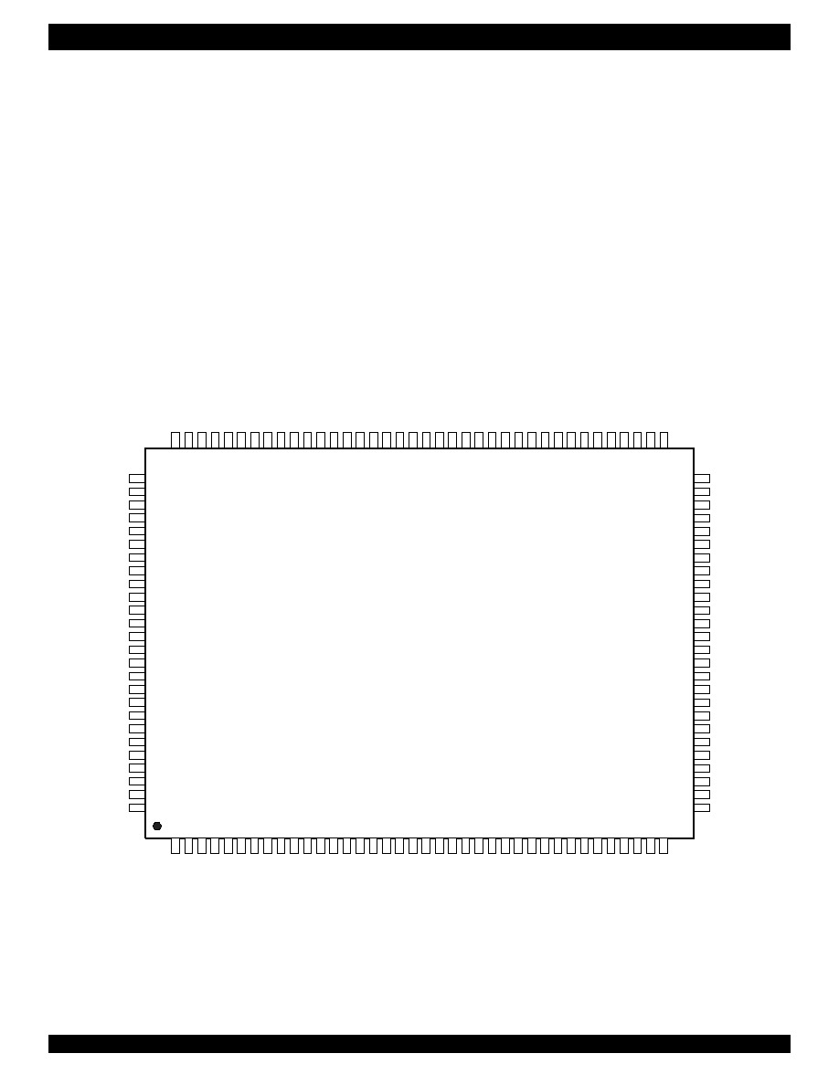
PIN CONFIGURATION
IOM
�
-2 is a registered trademark of Siemens AG.
IDT82V1068
128 PIN TQFP
SB1_5
SI2_5
SI1_5
VDD
5
6
SO3_6
SO2_6
SO1_6
SB2_6
SB1_6
SI2_6
SI1_6
VDD
A
S
CN
F2
VO
UT5
GN
DA5
VIN5
VDD
A
56
VIN6
GN
DA6
VO
UT6
VO
UT7
GN
DA7
VIN7
VDD
A
78
VIN8
GN
DA8
VO
UT8
SI1_7
SI2_7
SB1_7
SB2_7
SO1_7
102
101
100
99
98
97
96
95
94
93
92
91
90
89
88
87
86
85
84
83
82
81
80
79
78
77
76
75
74
73
72
71
SO2_7
SO3_7
VDD
7
8
SI1_8
SI2_8
SB1_8
70
69
68
67
66
65
SB2_5
SO1_5
SO2_5
SO3_5
GND56
MPI
CS
CCLK/TS
CI/DOUBLE
CO
INT
NC
NC
NC
NC
NC
NC
NC
NC
RESET
NC
GND12
SO3_1
SO2_1
SO1_1
SB2_1
103
104
105
106
107
108
109
110
111
112
113
114
115
116
117
118
119
120
121
122
123
124
125
126
127
128
64
63
62
61
60
59
58
57
56
55
54
53
52
51
50
49
48
47
46
45
44
43
42
41
40
39
SB2_8
SO1_8
SO2_8
SO3_8
GND78
GNDDP
NC
CHCLK1
CHCLK2
VDDDP
MCLK
BCLK/DCL
FS/FSC
NC
TSX2
DX2
DR2
TSX1
DX1/DU
DR1/DD
NC
GND34
SO3_4
SO2_4
SO1_4
SB2_4
1
2
3
4
5
6
7
8
9
10
11
12
13
14
15
16
17
18
19
20
21
22
23
24
25
26
27
28
29
30
31
32
33
34
35
36
37
38
SB
1_1
SI2_1
SI1_1
VD
D1
2
SO3_2
SO2_2
SO1_2
SB
2_2
SB
1_2
SI2_2
SI1_2
GN
DA
S
CN
F1
VO
U
T
1
G
NDA
1
VI
N1
VD
DA
12
VI
N2
G
NDA
2
VO
U
T
2
VO
U
T
3
G
NDA
3
VI
N3
VD
DA
34
VI
N4
G
NDA
4
VO
U
T
4
SI1_3
SI2_3
SB
1_3
SB
2_3
SO1_3
SO2_3
SO3_3
VD
D3
4
SI1_4
SI2_4
SB
1_4

IDT82V1068 OCTAL PROGRAMMABLE PCM CODEC INDUSTRIAL TEMPERATURE RANGE
3
TABLE OF CONTENTS
1
Pin Description...................................................................................................................................................................................................7
2
Function Description .......................................................................................................................................................................................11
2.1
MPI Mode and GCI Mode........................................................................................................................................................................11
2.1.1
MPI Control Interface .................................................................................................................................................................11
2.1.2
PCM Bus ....................................................................................................................................................................................11
2.1.3
GCI Mode ...................................................................................................................................................................................13
2.1.3.1 Compressed GCI Structure ........................................................................................................................................13
2.1.3.2 Linear GCI Structure...................................................................................................................................................14
2.1.4
C/I Channel ................................................................................................................................................................................15
2.1.4.1 Upstream C/I Channel ................................................................................................................................................15
2.1.4.2 Downstream C/I Channel ...........................................................................................................................................15
2.1.5
Monitor Channel .........................................................................................................................................................................15
2.1.5.1 Monitor Handshake ....................................................................................................................................................15
2.2
DSP Programming...................................................................................................................................................................................18
2.2.1
Signal Processing.......................................................................................................................................................................18
2.2.2
Gain Adjustment.........................................................................................................................................................................18
2.2.3
Impedance Matching ..................................................................................................................................................................18
2.2.4
Transhybrid Balance ..................................................................................................................................................................18
2.2.5
Frequency Response Correction................................................................................................................................................18
2.3
SLIC Control ............................................................................................................................................................................................20
2.3.1
SI1 and SI2.................................................................................................................................................................................20
2.3.2
SB1 and SB2..............................................................................................................................................................................20
2.3.3
SO1, SO2 and SO3...................................................................................................................................................................20
2.4
Hardware Ring Trip .................................................................................................................................................................................20
2.5
Interrupt and Interrupt Enable..................................................................................................................................................................20
2.6
Chopper Clock.........................................................................................................................................................................................21
2.7
Debounce Filters .....................................................................................................................................................................................21
2.8
Dual Tone and Ring Generation..............................................................................................................................................................21
2.9
FSK Signal Generation............................................................................................................................................................................22
2.9.1
Configure the FSK Generators...................................................................................................................................................22
2.9.2
FSK-RAM ...................................................................................................................................................................................22
2.9.3
Broadcasting Mode For FSK Configuration................................................................................................................................22
2.10 Level Metering .........................................................................................................................................................................................24
2.11 Channel Power Down/Standby Mode......................................................................................................................................................24
2.12 Power Down PLL/Suspend Mode............................................................................................................................................................24
3
Operating Description .....................................................................................................................................................................................25
3.1
Programming Description ........................................................................................................................................................................25
3.1.1
Broadcasting Mode for MPI Programming .................................................................................................................................25
3.1.2
Identification Code for MPI Mode ...............................................................................................................................................25
3.1.3
Program Start byte for GCI Mode...............................................................................................................................................25
3.1.4
Identification Command for GCI Mode .......................................................................................................................................25
3.1.5
Command Type and Format ......................................................................................................................................................25
3.1.6
Addressing Local Register .........................................................................................................................................................26
3.1.7
Addressing the Global Registers................................................................................................................................................26
3.1.8
Addressing the Coe-RAM...........................................................................................................................................................26
3.1.9
Addressing the FSK-RAM ..........................................................................................................................................................26
3.1.10 Examples of MPI Commands.....................................................................................................................................................27
3.1.11 Examples of GCI Commands.....................................................................................................................................................28
3.2
Power-on Sequence ................................................................................................................................................................................29
3.3
Default State After Reset.........................................................................................................................................................................29
3.4
Command List .........................................................................................................................................................................................30
3.4.1
Global Commands List ...............................................................................................................................................................30
3.4.2
Local Commands List.................................................................................................................................................................39
4
Absolute Maximum Ratings ............................................................................................................................................................................44

IDT82V1068 OCTAL PROGRAMMABLE PCM CODEC INDUSTRIAL TEMPERATURE RANGE
4
5
Recommended DC Operating Conditions .....................................................................................................................................................44
6
DC Electrical Characteristics..........................................................................................................................................................................44
6.1
Digital Interface........................................................................................................................................................................................44
6.2
Power Dissipation....................................................................................................................................................................................44
6.3
Analog Interface ......................................................................................................................................................................................45
7
AC Electrical Characteristics..........................................................................................................................................................................46
7.1
Absolute Gain ..........................................................................................................................................................................................46
7.2
Gain Tracking ..........................................................................................................................................................................................46
7.3
Frequency Response ..............................................................................................................................................................................46
7.4
Group Delay ............................................................................................................................................................................................47
7.5
Distortion .................................................................................................................................................................................................47
7.6
Noise .......................................................................................................................................................................................................48
7.7
Interchannel Crosstalk.............................................................................................................................................................................48
8
Timing Characteristics ....................................................................................................................................................................................49
8.1
Clock........................................................................................................................................................................................................49
8.2
Microprocessor Interface .........................................................................................................................................................................50
8.3
PCM Interface..........................................................................................................................................................................................51
8.4
GCI Interface ...........................................................................................................................................................................................52
9
Appendix: IDT82V1068 Coe-RAM Mapping ...................................................................................................................................................53
10 Ordering Information .......................................................................................................................................................................................55

IDT82V1068 OCTAL PROGRAMMABLE PCM CODEC INDUSTRIAL TEMPERATURE RANGE
5
LIST OF FIGURES
Figure 1
An Example of Serial Interface Write Mode ...................................................................................................................................... 11
Figure 2
An Example of Serial Interface Read Mode (ID = 81H)..................................................................................................................... 12
Figure 3
Sampling Edge Select Waveform...................................................................................................................................................... 12
Figure 4
Compressed GCI Frame Structure.................................................................................................................................................... 13
Figure 5
Linear GCI Frame Structure (TS = 0)................................................................................................................................................ 14
Figure 6
Monitor Channel Operation ............................................................................................................................................................... 16
Figure 7
State Diagram of the Monitor Transmitter ......................................................................................................................................... 16
Figure 8
State Diagram of the Monitor Receiver ............................................................................................................................................. 17
Figure 9
Signal Flow for Each Channel........................................................................................................................................................... 19
Figure 10
Debounce Filters ............................................................................................................................................................................... 21
Figure 11
General Procedure of Sending Caller-ID Signal................................................................................................................................ 22
Figure 12
A Recommended Programming Flow Chart for FSK Generator ....................................................................................................... 23
Figure 13
Clock Timing...................................................................................................................................................................................... 49
Figure 14
MPI Input Timing ............................................................................................................................................................................... 50
Figure 15
MPI Output Timing ............................................................................................................................................................................ 50
Figure 16
PCM Interface Timing........................................................................................................................................................................ 51
Figure 17
GCI Interface Timing ......................................................................................................................................................................... 52
Figure 18
Coe-RAM Address Mapping.............................................................................................................................................................. 53