
1
The IDT logo is a registered trademark of Integrated Device Technology, Inc.
INDUSTRIAL TEMPERATURE RANGE
2003 Integrated Device Technology, Inc.
FEBRUARY 16, 2004
DSC-6042/3
FEATURES
∑ Programmable DC feeding characteristics
∑ Programmable digital filters adapting to different requirements:
- Impedance matching
- Transhybrid balance
- Transmit and receive gain adjustment
- Frequency response correction
∑ Off-hook and ground-key detection
∑ AC/DC ring trip detection
∑ Programmable internal balanced ringing without external
components
∑ Supports external ringing
∑ Selectable MPI and GCI interfaces
∑ Supports A/µ-law compressed and linear data formats
∑ Programmable IO pins with relay-driving or analog input
capability
∑ Line polarity reversal
∑ Integrated FSK generator for sending Caller ID information
∑ On-hook transmission
∑ 2 programmable tone generators per channel
∑ Integrated Universal Tone Detection (UTD) unit for fax/modem
tone detection
∑ Integrated Test and Diagnosis Functions (ITDF)
∑ Three-party conference
∑ Only battery and 3.3 V power supply needed
∑ Package available:
IDT82V1671: 28 pin PLCC IDT82V1074: 100 pin TQFP
DESCRIPTION
The RSLIC-CODEC chipset is comprised of one four-channel
programmable PCM CODEC (IDT82V1074) and four single-channel
ringing SLICs (IDT82V1671). The chipset provides a total solution for
line card designs. In addition to providing a complete software
programmable solution for BORSCHT, additional functions such as FSK
generator, Universal Tone Detection (UTD) unit, tone generators, ringing
generator, Integrated Test and Diagnosis Functions (ITDF), line polarity
reversal and three-party conference are integrated in to the chipset. The
high integration of system functions reduces board space requirements
of the line card and saves cost.
The chipset is fully programmable via a Microprocessor Interface
(MPI) or a General Circuit Interface (GCI). In both MPI and GCI modes,
the chipset supports A/µ-law companding format or linear data format.
Programmable digital filters on the chipset provide the necessary
transmit and receive filtering to realize impedance matching, transhybrid
balance, frequency response correction and transmit/receive gains
adjustment. The full programmability optimizes the performance of line
card products and allows one line card to adapt to different requirements
worldwide.
The powerful Integrated Test and Diagnosis Functions (ITDF)
accomplish necessary tests and measurements without external test
equipment or relays. This brings convenience to system maintenance
and diagnosis.
This chipset can be used in digital telecommunication applications
such as VoIP, VoATM, PBX, CO and DLC etc.
CHIPSET FUNCTIONAL BLOCK DIAGRAM
RSLIC
1
#
RSLIC
2
#
RSLIC
3
#
RSLIC
4
#
Level
Metering
Off-hook
Detection
DC Feed
DSP
Filtering
MPI
Interface
PCM/GCI
Interface
CID
UTD
Self Test
CODEC
PCM/GCI
Telephone
Telephone
Telephone
Telephone
Protection
Circuit
Protection
Circuit
Protection
Circuit
Protection
Circuit
Microprocessor
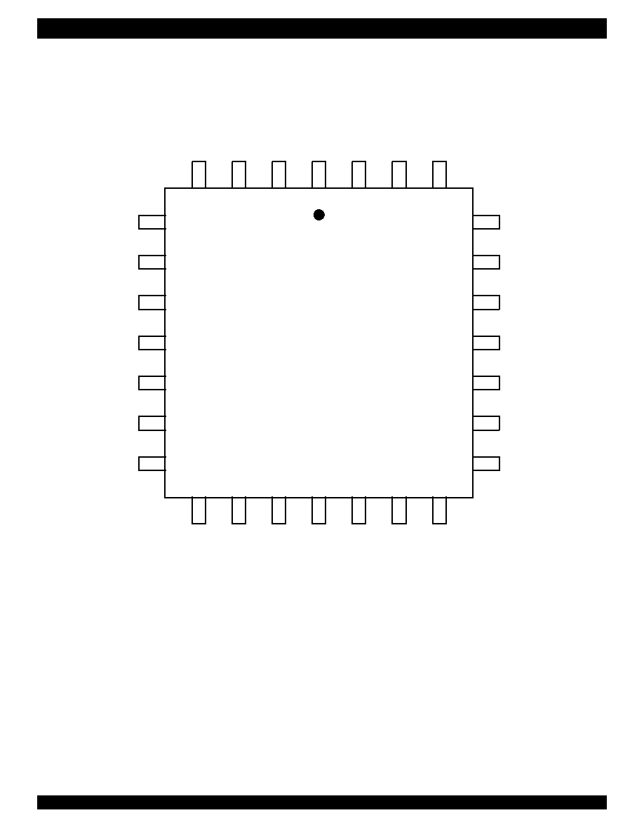
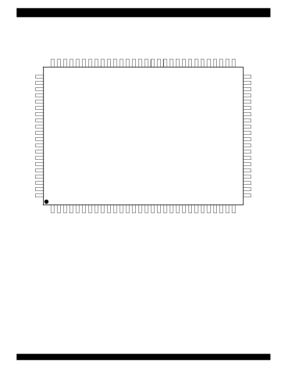
CHIPSET OF RINGING SUBSCRIBER
LINE INTERFACE CIRCUIT (RSLIC) &
QUAD PROGRAMMABLE PCM CODEC
IDT82V1671 (RSLIC)
IDT82V1074 (CODEC)

2
RSLIC (IDT82V1671) & CODEC (IDT82V1074) CHIPSET INDUSTRIAL TEMPERATURE RANGE
RSLIC FUNCTIONAL BLOCK DIAGRAM
Battery
Switch
Line
Driver
Ring
Trip
IL
Sense
IT
Sense
Input
Stage
Logic
Control
VBL VBH
VCM
VDD
GND
VL
VTDC
VTAC
CA
ACN
ACP
DCN
DCP
CS
M1
M2
M3
RT
RSN
RSP
TIP
RING
TIS
RIS

3
RSLIC (IDT82V1671) & CODEC (IDT82V1074) CHIPSET INDUSTRIAL TEMPERATURE RANGE
CODEC FUNCTIONAL BLOCK DIAGRAM
Filter and A/D for AC
D/A and Filter for AC
General Control
Logic
Filter and A/D for DC
D/A and Filter for DC
SLIC Signaling
Channel1 for AC
Channel1 for DC
DSP CORE
Channel2 for AC
Channel3 for AC
Channel4 for AC
Channel2 for DC
Channel3 for DC
Channel4 for DC
PLL and Clock
Generation
MPI Interface
PCM/GCI Interface
MPI/GCI
RESET
DR1/DD
DR2
DX1/DU
DX2
FSC BCLK/DCL TSX1 TSX2
CCLK/S0
CI/S1
CO
CS
MCLK
4 I/Os
CS1
ACP1
ACN1
VTAC1
VTDC1
DCP1
DCN1
SLIC Interface
Control
M1
M2
M3
INT/INT

4
RSLIC (IDT82V1671) & CODEC (IDT82V1074) CHIPSET INDUSTRIAL TEMPERATURE RANGE
TABLE OF CONTENTS
1
Pin Configurations .............................................................................................................................................................................................9
1.1
RSLIC Pin Configuration ...........................................................................................................................................................................9
1.2
CODEC Pin Configuration .......................................................................................................................................................................10
2
Pin Descriptions...............................................................................................................................................................................................11
2.1
RSLIC Pin Description.............................................................................................................................................................................11
2.2
CODEC Pin Description ..........................................................................................................................................................................12
3
Functional Description ....................................................................................................................................................................................16
3.1
Functions Overview .................................................................................................................................................................................16
3.1.1
Basic Functions ..........................................................................................................................................................................16
3.1.2
Additional Functions ...................................................................................................................................................................16
3.1.3
Programmable Functions ...........................................................................................................................................................16
3.2
DC Feeding .............................................................................................................................................................................................17
3.2.1
DC Feeding Characteristic Zones ..............................................................................................................................................17
3.2.2
Constant Current Zone...............................................................................................................................................................17
3.2.3
Resistive Zone............................................................................................................................................................................17
3.2.4
Constant Voltage Zone...............................................................................................................................................................17
3.2.5
DC Feeding Characteristics Configuration .................................................................................................................................18
3.3
Speech Processing..................................................................................................................................................................................20
3.3.1
AC Transmission ........................................................................................................................................................................20
3.3.1.1 Transmit Path ............................................................................................................................................................20
3.3.1.2 Receive Path ..............................................................................................................................................................21
3.3.2
Programmable Filters .................................................................................................................................................................21
3.3.2.1 Impedance Matching ..................................................................................................................................................21
3.3.2.2 Transhybrid Balance...................................................................................................................................................22
3.3.2.3 Frequency Response Correction................................................................................................................................22
3.3.2.4 Gain Adjustment .........................................................................................................................................................22
3.4
Ring and Ring Trip...................................................................................................................................................................................23
3.4.1
Internal Ringing Mode ................................................................................................................................................................23
3.4.1.1 Internal Ringing Generation........................................................................................................................................23
3.4.1.2 Ring Trip Detection In Internal Ringing Mode.............................................................................................................23
3.4.2
External Ringing Mode ...............................................................................................................................................................24
3.4.2.1 Ring Trip Detection In External Ringing Mode............................................................................................................25
3.5
Supervision..............................................................................................................................................................................................27
3.5.1
Off-hook Detection .....................................................................................................................................................................27
3.5.2
Ground-Key Detection................................................................................................................................................................29
3.6
Metering by Polarity Reversal..................................................................................................................................................................29
3.7
Enhanced Signal Processing...................................................................................................................................................................30
3.7.1
Tone Generator ..........................................................................................................................................................................30
3.7.1.1 DTMF Generation.......................................................................................................................................................30
3.7.2
FSK Generation for Caller ID .....................................................................................................................................................30
3.7.3
Universal Tone Detection (UTD) ................................................................................................................................................34
3.7.3.1 Introduction.................................................................................................................................................................34
3.7.3.2 UTD Principle .............................................................................................................................................................34
3.7.3.3 UTD Programming......................................................................................................................................................36
3.8
Three-Party Conference ..........................................................................................................................................................................37
3.8.1
Introduction.................................................................................................................................................................................37
3.8.2
PCM Interface Configuration ......................................................................................................................................................37
3.8.3
Control the Active PCM Channels..............................................................................................................................................38
3.9
ITDF.........................................................................................................................................................................................................40
3.9.1
Introduction.................................................................................................................................................................................40
3.9.2
Diagnosis and Test Functions ....................................................................................................................................................40
3.9.3
Integrated Signal Generators .....................................................................................................................................................40
3.9.4
Level Meter.................................................................................................................................................................................40
3.9.4.1 Level Meter Source Selection.....................................................................................................................................40

5
RSLIC (IDT82V1671) & CODEC (IDT82V1074) CHIPSET INDUSTRIAL TEMPERATURE RANGE
3.9.4.2 Level Meter Gain Filter and Rectifier ..........................................................................................................................41
3.9.4.3 Level Meter Integrator ................................................................................................................................................42
3.9.4.4 Level Meter Result Register .......................................................................................................................................43
3.9.4.5 Level Meter Shift Factor .............................................................................................................................................43
3.9.4.6 Level Meter Threshold Setting....................................................................................................................................43
3.9.5
Measurement via AC Level Meter ..............................................................................................................................................45
3.9.5.1 Current Measurement via VTAC.................................................................................................................................45
3.9.5.2 AC Level Meter Operational State Flow .....................................................................................................................45
3.9.6
Measurement via DC Level Meter..............................................................................................................................................45
3.9.6.1 Offset Current Measurement ......................................................................................................................................45
3.9.6.2 Leakage Current Measurement..................................................................................................................................45
3.9.6.3 Loop Resistance Measurement..................................................................................................................................46
3.9.6.4 Line Resistance Tip/GND and Ring/GND...................................................................................................................46
3.9.6.5 Capacitance Measurement.........................................................................................................................................47
3.9.6.6 Voltage Measurement ................................................................................................................................................48
3.9.6.7 Voltage Offset Measurement......................................................................................................................................49
3.9.6.8 Ring Trip Operational Amplifier Offset Measurement.................................................................................................49
4
Interface ............................................................................................................................................................................................................50
4.1
PCM/MPI Interface ..................................................................................................................................................................................50
4.1.1
MPI Control Interface .................................................................................................................................................................50
4.1.2
PCM Interface ............................................................................................................................................................................51
4.1.2.1 PCM Clock Configuration ...........................................................................................................................................51
4.1.2.2 Time Slot Assignment.................................................................................................................................................52
4.1.2.3 PCM Highway Selection .............................................................................................................................................52
4.2
GCI Interface ...........................................................................................................................................................................................52
4.2.1
Compressed GCI Mode..............................................................................................................................................................52
4.2.2
Linear GCI Mode ........................................................................................................................................................................52
4.2.3
Command/Indication (C/I) Channel ............................................................................................................................................55
4.2.3.1 Downstream C/I Channel Byte ...................................................................................................................................55
4.2.3.2 Upstream C/I Channel Byte........................................................................................................................................55
4.2.4
GCI Monitor Transfer Protocol....................................................................................................................................................56
4.2.4.1 Monitor Channel Operation ........................................................................................................................................56
4.2.4.2 Monitor Handshake Procedure...................................................................................................................................56
4.3
Analog POTS Interface............................................................................................................................................................................58
4.4
RSLIC and CODEC Interface ..................................................................................................................................................................58
5
Programming....................................................................................................................................................................................................59
5.1
Overview..................................................................................................................................................................................................59
5.1.1
MPI Programming ......................................................................................................................................................................59
5.1.1.1 Broadcast Mode for MPI Programming ......................................................................................................................59
5.1.1.2 Identification Code for MPI Programming...................................................................................................................59
5.1.2
GCI Programming ......................................................................................................................................................................59
5.1.2.1 Program Start Byte for GCI Programming..................................................................................................................59
5.1.2.2 Identification Command for GCI Programming...........................................................................................................59
5.2
Register/RAM Commands.......................................................................................................................................................................59
5.2.1
Register/RAM Command Format ...............................................................................................................................................59
5.2.2
Addressing the Local Registers..................................................................................................................................................59
5.2.3
Addressing the Global Registers................................................................................................................................................60
5.2.4
Addressing the FSK-RAM ..........................................................................................................................................................60
5.2.5
Addressing the Coe-RAM...........................................................................................................................................................61
5.3
Registers Description ..............................................................................................................................................................................63
5.3.1
Registers Overview ....................................................................................................................................................................63
5.3.2
Global Registers List ..................................................................................................................................................................65
5.3.3
Local Registers List ....................................................................................................................................................................73
5.4
Programming Examples ..........................................................................................................................................................................83
5.4.1
Programming Examples for MPI Mode.......................................................................................................................................83
5.4.1.1 Example of Programming the Local Registers via MPI ..............................................................................................83

6
RSLIC (IDT82V1671) & CODEC (IDT82V1074) CHIPSET INDUSTRIAL TEMPERATURE RANGE
5.4.1.2 Example of Programming the Global Registers via MPI.............................................................................................84
5.4.1.3 Example of Programming the Coefficient-RAM via MPI.............................................................................................84
5.4.1.4 Example of Programming the FSK-RAM via MPI.......................................................................................................84
5.4.2
Programming Examples for GCI Mode.......................................................................................................................................85
5.4.2.1 Example of Programming the Local Registers via GCI ..............................................................................................85
5.4.2.2 Example of Programming the Global Registers via GCI.............................................................................................85
5.4.2.3 Example of Programming the Coefficient-RAM via GCI.............................................................................................85
5.4.2.4 Example of Programming the FSK-RAM via GCI.......................................................................................................86
6
Operational Description ..................................................................................................................................................................................87
6.1
Operating Modes .....................................................................................................................................................................................87
6.1.1
RSLIC Control Signaling ............................................................................................................................................................87
6.1.2
RSLIC Operating Modes ............................................................................................................................................................89
6.1.3
CODEC Operating Modes..........................................................................................................................................................89
6.2
PLL Power Down.....................................................................................................................................................................................90
6.3
Programmable I/Os of the CODEC .........................................................................................................................................................90
6.4
Interrupt Handling ....................................................................................................................................................................................91
6.5
Signal Path and Test Loopbacks.............................................................................................................................................................91
6.6
RSLIC Power On Sequence....................................................................................................................................................................93
6.7
CODEC Power On Sequence .................................................................................................................................................................93
6.8
Default State After Reset.........................................................................................................................................................................93
6.8.1
Power-On Reset and Hardware Reset.......................................................................................................................................93
6.8.2
Software Reset...........................................................................................................................................................................93
7
Electrical Characteristics ................................................................................................................................................................................94
7.1
RSLIC Electrical Characteristics..............................................................................................................................................................94
7.1.1
RSLIC Absolute Maximum Ratings ............................................................................................................................................94
7.1.2
RSLIC Recommended Operating Conditions.............................................................................................................................94
7.1.3
RSLIC Thermal Information........................................................................................................................................................94
7.1.4
RSLIC Power Consumption .......................................................................................................................................................94
7.2
CODEC Electrical Characteristics ...........................................................................................................................................................95
7.2.1
CODEC Absolute Maximum Ratings..........................................................................................................................................95
7.2.2
CODEC Recommended Operating Conditions ..........................................................................................................................95
7.2.3
CODEC Digital Interface ............................................................................................................................................................95
7.2.4
CODEC Power Dissipation.........................................................................................................................................................95
7.3
Chipset Transmission Characteristics .....................................................................................................................................................96
7.3.1
Absolute Gain.............................................................................................................................................................................96
7.3.2
Gain Tracking .............................................................................................................................................................................96
7.3.3
Frequency Response .................................................................................................................................................................96
7.3.4
Return Loss ................................................................................................................................................................................96
7.3.5
Group Delay ...............................................................................................................................................................................97
7.3.6
Distortion ....................................................................................................................................................................................97
7.3.7
Noise ..........................................................................................................................................................................................97
7.3.8
Interchannel Crosstalk................................................................................................................................................................98
7.4
CODEC Timing Characteristics ...............................................................................................................................................................99
7.4.1
Clock Timing...............................................................................................................................................................................99
7.4.2
Microprocessor Interface Timing ..............................................................................................................................................100
7.4.3
PCM Interface Timing...............................................................................................................................................................101
7.4.4
GCI Interface Timing ................................................................................................................................................................103
8
Application Circuits .......................................................................................................................................................................................104
8.1
Application Circuit for the Internal Ringing Mode ..................................................................................................................................104
8.2
Application Circuit for the External Ringing Mode .................................................................................................................................105
9
Ordering Information .....................................................................................................................................................................................106

7
RSLIC (IDT82V1671) & CODEC (IDT82V1074) CHIPSET INDUSTRIAL TEMPERATURE RANGE
LIST OF FIGURES
Figure - 1
Line Circuit Functions Included in the RSLIC-CODEC Chipset ........................................................................................................ 16
Figure - 2
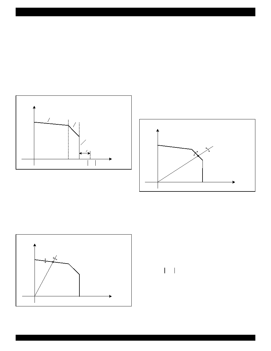
DC Feeding Zones ............................................................................................................................................................................ 17
Figure - 3
Constant Current Zone...................................................................................................................................................................... 17
Figure - 4
Resistive Zone................................................................................................................................................................................... 17
Figure - 5
Constant Voltage Zone...................................................................................................................................................................... 18
Figure - 6
DC Feeding Characteristics Configuration ........................................................................................................................................ 18
Figure - 7
DC Feeding Configuration Example for Short Loop Applications...................................................................................................... 18
Figure - 8
Signal Paths for AC Transmission..................................................................................................................................................... 20
Figure - 9
Voice Signal Path of the CODEC...................................................................................................................................................... 20
Figure - 10
Nyquist Diagram................................................................................................................................................................................ 21
Figure - 11
Internal Balanced Ringing ................................................................................................................................................................. 23
Figure - 12
External Ringing Synchronization ..................................................................................................................................................... 25
Figure - 13
Hysteresis for Off-Hook Detection..................................................................................................................................................... 27
Figure - 14
Debounce Filter for Off-hook/Ground-key Detection ......................................................................................................................... 28
Figure - 15
FSK Signal Transmission Sequence................................................................................................................................................. 31
Figure - 16
Recommended Programming Flow Chart for FSK Generation ......................................................................................................... 33
Figure - 17
UTD Functional Diagram................................................................................................................................................................... 34
Figure - 18
Example of UTD Recognition Timing ................................................................................................................................................ 35
Figure - 19
Example of UTD Tone End Detection Timing ................................................................................................................................... 35
Figure - 20
Conference Block Diagram ............................................................................................................................................................... 37
Figure - 21
Level Meter Block Diagram ............................................................................................................................................................... 41
Figure - 22
Continuous Measurement Sequence (AC & DC Level Meter) .......................................................................................................... 42
Figure - 23
Single Measurement Sequence (AC & DC Level Meter) .................................................................................................................. 42
Figure - 24
Example for Resistance Measurement ............................................................................................................................................. 46
Figure - 25
Differential Resistance Measurement ............................................................................................................................................... 46
Figure - 26
Capacitance Measurement ............................................................................................................................................................... 47
Figure - 27
External Voltage Measurement Principle .......................................................................................................................................... 48
Figure - 28
MPI Read Operation Timing.............................................................................................................................................................. 50
Figure - 29
MPI Write Operation Timing .............................................................................................................................................................. 50
Figure - 30
PCM Clock Slope Select Waveform.................................................................................................................................................. 51
Figure - 31
Compressed GCI Frame Structure.................................................................................................................................................... 53
Figure - 32
Linear GCI Frame Structure .............................................................................................................................................................. 54
Figure - 33
Monitor Channel Operation ............................................................................................................................................................... 56
Figure - 34
State Diagram of the Monitor Transmitter ......................................................................................................................................... 57
Figure - 35
State Diagram of the Monitor Receiver ............................................................................................................................................. 58
Figure - 36
Waveform of Programming Example: Writing to Local Registers ..................................................................................................... 83
Figure - 37
Waveform of Programming Example: Reading Local Registers ....................................................................................................... 83
Figure - 38
RSLIC Mode Control Signaling ......................................................................................................................................................... 87
Figure - 39
RSLIC Control Timing Diagram......................................................................................................................................................... 88
Figure - 40
RSLIC Internal Test Circuit................................................................................................................................................................ 89
Figure - 41
IO Debounce Filter ............................................................................................................................................................................ 90
Figure - 42
AC/DC Signal Path and Test Loopbacks .......................................................................................................................................... 92
Figure - 43
Clock Timing...................................................................................................................................................................................... 99
Figure - 44
MPI Input Timing ............................................................................................................................................................................. 100
Figure - 45
MPI Output Timing .......................................................................................................................................................................... 100
Figure - 46
PCM Interface Timing (Single Clock Mode) .................................................................................................................................... 101
Figure - 47
PCM Interface Timing (Double Clock Mode)................................................................................................................................... 102
Figure - 48
GCI Interface Timing ....................................................................................................................................................................... 103
Figure - 49
Application Circuit for the Internal Ringing Mode ............................................................................................................................ 104
Figure - 50
Application Circuit for the External Ringing Mode ........................................................................................................................... 105

8
RSLIC (IDT82V1671) & CODEC (IDT82V1074) CHIPSET INDUSTRIAL TEMPERATURE RANGE
LIST OF TABLES
Table - 1
Registers and Coe-RAM Locations Used for DC Feeding Configuration...........................................................................................19
Table - 2
Registers and Coe-RAM Locations Used for Internal Ringing Mode .................................................................................................24
Table - 3
Registers and Coe-RAM Locations Used for External Ringing Mode ................................................................................................26
Table - 4
Off-hook Detection in Different Modes ...............................................................................................................................................27
Table - 5
Registers and Coe-RAM Locations Used for Off-hook Detection ......................................................................................................28
Table - 6
Registers Used for Ground-key Detection..........................................................................................................................................29
Table - 7
Registers and Coe-RAM Locations Used for Tone Generation .........................................................................................................30
Table - 8
FSK Modulation Characteristics.........................................................................................................................................................31
Table - 9
Registers and FSK-RAM Used for the FSK Generator ......................................................................................................................32
Table - 10
Registers and Coe-RAM Locations Used for UTD .............................................................................................................................36
Table - 11
Conference Mode...............................................................................................................................................................................38
Table - 12
Active PCM Channel Configuration Bits.............................................................................................................................................38
Table - 13
Level Meter Source Selection ............................................................................................................................................................40
Table - 14
Level Meter Result Value Range........................................................................................................................................................43
Table - 15
Shift Factor Selection .........................................................................................................................................................................43
Table - 16
Level Meter Threshold Setting ...........................................................................................................................................................43
Table - 17
Registers and Coe-RAM Locations Used for the Level Meter............................................................................................................44
Table - 18
Registers and Coe-RAM Locations Used for Ramp Generator..........................................................................................................48
Table - 19
Time Slot Selection For Compressed GCI .........................................................................................................................................53
Table - 20
Time Slot Selection For Linear GCI....................................................................................................................................................54
Table - 21
Local Register Addressing in MPI Mode ............................................................................................................................................60
Table - 22
Local Register Addressing in GCI Mode ............................................................................................................................................60
Table - 23
Coefficient RAM Mapping...................................................................................................................................................................62
Table - 24
Global Registers Mapping ..................................................................................................................................................................63
Table - 25
Local Registers Mapping....................................................................................................................................................................64
Table - 26
RSLIC Operating Mode......................................................................................................................................................................89
Table - 27
Interrupt Source and Interrupt Mask...................................................................................................................................................91
Table - 28
External Components in Application Circuits ...................................................................................................................................105
9
RSLIC (IDT82V1671) & CODEC (IDT82V1074) CHIPSET INDUSTRIAL TEMPERATURE RANGE
1
PIN CONFIGURATIONS
1.1
RSLIC PIN CONFIGURATION
IDT82V1671
IDT82V1671
VBH
VBL
TIP
RI
NG
1
28
27
26
2
3
4
RI
S
BG
ND
TIS
19
20
21
22
23
24
25
18
17
16
15
14
13
12
5
6
7
8
9
10
11
M2
M1
CS
RT
RSN
RSP
VCMB
M3
CB
VL
VTDC
CA
VTAC
DCP
VDD
AGND
CF
VCM
ACN
ACP
DCN
10
RSLIC (IDT82V1671) & CODEC (IDT82V1074) CHIPSET INDUSTRIAL TEMPERATURE RANGE
1.2
CODEC PIN CONFIGURATION
VDDA4
IO1_3
IO4_3
IO3_3
IO2_3
IOGND
IO4_4
IO3_4
IO2_4
IO1_4
76
77
78
79
80
81
82
83
84
85
86
87
88
89
90
91
92
93
94
95
96
97
98
99
100
1
2
3
4
5
6
7
8
9
10
11
12
13
14
15
16
17
18
19
20
21
22
23
24
25
26
27
28
29
30
31
32
33
34
35
36
37
38
39
40
41
42
43
44
45
46
47
48
49
50
51
52
53
54
55
56
57
58
59
60
61
62
63
64
65
66
67
68
69
70
71
72
73
74
75
ACN1
VTDC1
DCN1
VL1
VTAC1
AGND
DCP1
CA1_1
CA2_1
ACP1
IO4_2
IO3_2
IO2_2
IO1_2
IOGND
IO4_1
IO3_1
IO2_1
IO1_1
RTIN1
AC
N4
AC
P
3
AGN
D
AC
N3
AGN
D
C
A
1_3
C
A
2_3
DC
N3
DC
P
3
VTA
C
3
VTD
C
3
VL3
RTI
N
3
VD
D
A
3
CN
F
AGN
D
VTA
C
2
VTD
C
2
VL2
VD
D
A
2
VC
M
C
A
1_2
DC
P
2
RTI
N
2
VD
D
B
DR
2
DX
1/
D
U
FSC
VD
D
D
TSX
2
DX
2
DR
1/
D
D
TSX
1
R
ESE
T
MC
LK
DG
ND
DG
ND
RS
Y
N
C
MPI
/G
C
I
CI
/
S
1
M2
M3
TES
T
M1
CC
L
K
/
S
0
CS
2
CS
1
C0
VD
D
D
CS
AGND
DCP4
CA1_4
VL4
VTDC4
VTAC4
RTIN4
ACP4
CA2_4
DCN4
IDT82V1074
VD
D
A
1
DC
N2
AC
P
2
AC
N2
C
A
2_2
CS
3
DC
L
/
BCL
K
IN
T
/I
N
T
VD
D
I
O
CS
4
11
RSLIC (IDT82V1671) & CODEC (IDT82V1074) CHIPSET INDUSTRIAL TEMPERATURE RANGE
2
PIN DESCRIPTIONS
2.1
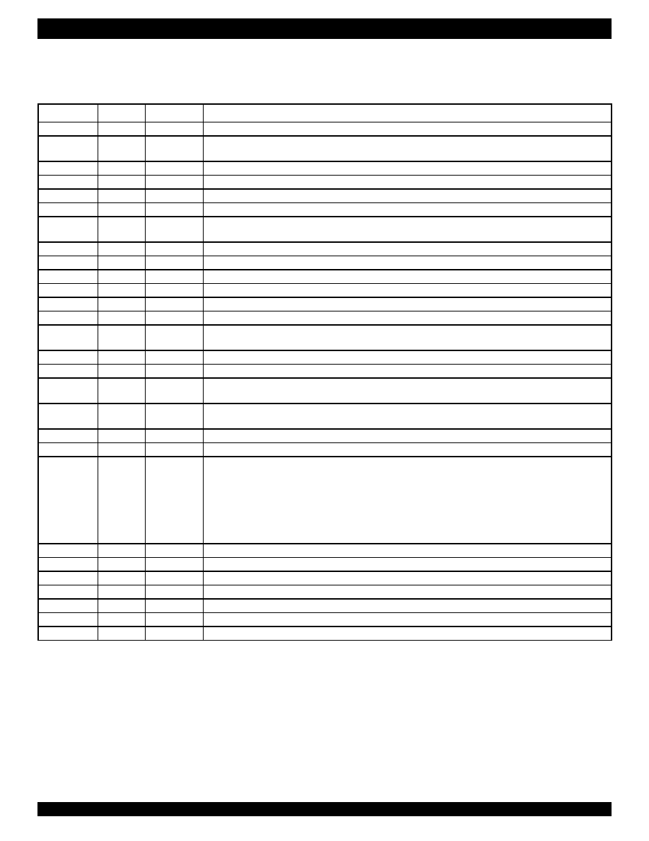
RSLIC PIN DESCRIPTION
Name
Type
Pin Number
Description
VBH
Power
1
Negative battery supply (
-70 V VBH -52 V)
RIS
-
2
Ring sense, connected to the RING pin through an external resistor R
S
. Refer to
"8 Application Circuits" on page 104
for details.
BGND
Power
3
Battery ground. This pin should be externally connected to AGND.
TIS
-
4
Tip sense, connected to the TIP pin through an external resistor R
S
.
VDD
Power
5
+3.3 V power supply.
AGND
Power
6
Analog ground. This pin should be externally connected to BGND.
CF
7
Output voltage of VBAT/2 (VBAT represents the selected battery voltage VBH or VBL). An external capacitor is
connected between this pin and the ground for filtering.
VCM
I
8
Reference voltage input, typical 1.5 V.
ACN
I
9
Differential AC voltage, negative.
ACP
I
10
Differential AC voltage, positive.
DCN
I
11
Differential DC voltage, negative.
DCP
I
12
Differential DC voltage, positive.
VTAC
O
13
Sense transversal AC voltage.
CA
-
14
External capacitor connection. An external capacitor is connected between this pin and the CB pin to separate the DC
component from the sense transversal voltage.
VTDC
O
15
Sense transversal DC voltage.
VL
O
16
Sense longitudinal voltage.
CB
-
17
External capacitor connection. An external capacitor is connected between this pin and the CA pin to separate the DC
component from the sense transversal voltage.
M3
I/O
18
Mode control input 3 or temperature information output.
The logic level of the CS pin determines the direction of the M3 pin. See the description of the CS pin for details.
M2
I
19
Mode control input 2. This is a binary logic pin, together with M1 and M3, controlling the operating mode of the RSLIC.
M1
I
20
Mode control input 1. This is a binary logic pin, together with M2 and M3, controlling the operating mode of the RSLIC.
CS
I
21
Chip select input. It is a ternary logic pin.
When the CS pin is logic
0 (0 V< CS < 0.8 V)
, the RSLIC receives the mode control data from the CODEC through
the M1 to M3 pins.
When the CS pin is logic 1
(2.2 V< CS < 3.3 V)
, the RSLIC sends the temperature information of itself to the
CODEC through the M3 pin.
When the CS pin is 1.5 V (with
±0.5 V tolerance
), the RSLIC neither receives the data from the CODEC nor sends
temperature information to it.
RT
O
22
Ring trip operational amplifier output.
RSN
I
23
Negative ring trip operational amplifier input.
RSP
I
24
Positive ring trip operational amplifier input.
VCMB
O
25
VCM buffer output, 1.5 V, used for external ringing mode.
RING
I/O
26
Subscriber loop connection Ring.
TIP
I/O
27
Subscriber loop connection Tip.
VBL
Power
28
Negative battery supply (
-52 V VBL -20 V).

12
RSLIC (IDT82V1671) & CODEC (IDT82V1074) CHIPSET INDUSTRIAL TEMPERATURE RANGE
2.2
CODEC PIN DESCRIPTION
Name
Type
Pin Number
Description
VTDC1
I
33
DC component of the transversal voltage (Channel 1).
VTAC1
I
34
AC component of transversal voltage (Channel 1).
VL1
I
32
Longitudinal voltage (Channel 1).
RTIN1
I
31
Analog voltage that can be used for external ring trip detection (channel 1).
ACP1
O
40
Differential AC voltage, positive (Channel 1).
ACN1
O
41
Differential AC voltage, negative (Channel 1).
DCP1
O
36
Differential DC voltage, positive (Channel 1).
DCN1
O
39
Differential DC voltage, negative (Channel 1).
CS1
O
52
Ternary logic output 1, controlling the operating mode of the RSLIC1 (Channel 1).
When the CS1 pin is logic 0
(0 V< CS1 < 0.8 V)
, the CODEC sends mode control data to the RSLIC1 through the M1 to M3
pins.
When the CS1 pin is logic 1
(2.2 V< CS1 < 3.3 V)
, the CODEC receives the temperature information of the RSLIC1 through
the M3 pin.
When the CS1 pin is 1.5 V (with
±0.5 V tolerance
), no mode control data or temperature information is transferred between
the CODEC and the RSLIC1.
IO1_1
I/O
50
Programmable IO pin with relay-driving capability (Channel 1). In external ringing mode, the IO1_1 pin can be used to control
the external ring relay.
IO2_1
I/O
49
Programmable IO pin with relay-driving capability (Channel 1).
IO3_1
I/O
48
Programmable IO pin with analog input functionality (Channel 1).
IO4_1
I/O
47
Programmable IO pin with analog input functionality (Channel 1).
CA1_1
I/O
37
External capacitor connection. An external capacitor is connected between this pin and the DCP1 pin for filtering (Channel 1).
CA2_1
I/O
38
External capacitor connection. An external capacitor is connected between this pin and the DCN1 pin for filtering (Channel 1).
VTDC2
I
21
DC component of the transversal voltage (Channel 2).
VTAC2
I
22
AC component of the transversal voltage (Channel 2).
VL2
I
20
Longitudinal voltage (Channel 2).
RTIN2
I
19
Analog voltage that can be used for external ring trip detection (channel 2).
ACP2
O
28
Differential AC voltage, positive (Channel 2).
ACN2
O
29
Differential AC voltage, negative (Channel 2).
DCP2
O
24
Differential DC voltage, positive (Channel 2).
DCN2
O
27
Differential DC voltage, negative (Channel 2).
CS2
O
51
Ternary logic output 2, controlling the operating mode of the RSLIC2 (Channel 2).
When the CS2 pin is logic 0
(0 V< CS2 < 0.8 V)
, the CODEC sends mode control data to the RSLIC2 through the M1 to M3
pins.
When the CS2 pin is logic 1
(2.2 V< CS2 < 3.3 V)
, the CODEC receives the temperature information of the RSLIC2 through
the M3 pin.
When the CS2 pin is 1.5 V (with
±0.5 V tolerance
), no mode control data or temperature information is transferred between
the CODEC and the RSLIC2.
IO1_2
I/O
45
Programmable IO pin with relay-driving capability (Channel 2). In external ringing mode, the IO1_2 pin can be used to control
the external ring relay.
IO2_2
I/O
44
Programmable IO pin with relay-driving capability (Channel 2).
IO3_2
I/O
43
Programmable IO pin with analog input functionality (Channel 2).
IO4_2
I/O
42
Programmable IO pin with analog input functionality (Channel 2).
CA1_2
I/O
25
External capacitor connection. An external capacitor is connected between this pin and the DCP2 pin for filtering (Channel 2).
CA2_2
I/O
26
External capacitor connection. An external capacitor is connected between this pin and the DCN2 pin for filtering (Channel 2).

13
RSLIC (IDT82V1671) & CODEC (IDT82V1074) CHIPSET INDUSTRIAL TEMPERATURE RANGE
VTDC3
I
5
DC component of the transversal voltage (Channel 3).
VTAC3
I
6
AC component of the transversal voltage (Channel 3).
VL3
I
4
Longitudinal voltage (Channel 3).
RTIN3
I
3
Analog voltage that can be used for external ring trip (channel 3).
ACP3
O
12
Differential AC voltage, positive (Channel 3).
ACN3
O
13
Differential AC voltage, negative (Channel 3).
DCP3
O
8
Differential DC voltage, positive (Channel 3).
DCN3
O
11
Differential DC voltage, negative (Channel 3).
CS3
O
80
Ternary logic output 3, controlling the operating mode of the RSLIC3 (Channel 3).
When the CS3 pin is logic 0
(0 V< CS3 < 0.8 V)
, the CODEC sends mode control data to the RSLIC3 through the M1 to M3
pins.
When the CS3 pin is logic 1
(2.2 V< CS3 < 3.3 V)
, the CODEC receives the temperature information of the RSLIC3 through
the M3 pin.
When the CS3 pin is 1.5 V (with
±0.5 V tolerance
), no mode control data or temperature information is transferred between
the CODEC and the RSLIC3.
IO1_3
I/O
86
Programmable IO pin with relay-driving capability (Channel 3). In external ringing mode, the IO1_3 pin can be used to control
the external ring relay.
IO2_3
I/O
87
Programmable IO pin with relay-driving capability (Channel 3).
IO3_3
I/O
88
Programmable IO pin with analog input functionality (Channel 3).
IO4_3
I/O
89
Programmable IO pin with analog input functionality (Channel 3).
CA1_3
I/O
9
External capacitor connection. An external capacitor is connected between this pin and the DCP3 pin for filtering (Channel 3).
CA2_3
I/O
10
External capacitor connection. An external capacitor is connected between this pin and the DCN3 pin for filtering (Channel 3).
VTDC4
I
93
DC component of the transversal voltage (Channel 4).
VTAC4
I
94
AC component of the transversal voltage (Channel 4).
VL4
I
92
Longitudinal voltage (Channel 4).
RTIN4
I
91
Analog voltage that can be used for external ring trip (Channel 4).
ACP4
O
100
Differential AC voltage, positive (Channel 4).
ACN4
O
1
Differential AC voltage, negative (Channel 4).
DCP4
O
96
Differential DC voltage, positive (Channel 4).
DCN4
O
99
Differential DC voltage, negative (Channel 4).
CS4
O
79
Ternary logic output 4, controlling the operating mode of the RSLIC4 (Channel 4).
When the CS4 pin is logic 0
(0 V< CS4 < 0.8 V)
, the CODEC sends mode control data to the RSLIC4 through the M1 to M3
pins.
When the CS4 pin is logic 1
(2.2 V< CS4 < 3.3 V)
, the CODEC receives the temperature information of the RSLIC4 through
the M3 pin.
When the CS4 pin is 1.5 V (with
±0.5 V tolerance
), no mode control data or temperature information is transferred between
the CODEC and the RSLIC4.
IO1_4
I/O
81
Programmable IO pin with relay-driving capability (Channel 4). In external ringing mode, the IO1_4 pin can be used to control
the external ring relay.
IO2_4
I/O
82
Programmable IO pin with relay-driving capability (Channel 4).
IO3_4
I/O
83
Programmable IO pin with analog input functionality (Channel 4).
IO4_4
I/O
84
Programmable IO pin with analog input functionality (Channel 4).
CA1_4
I/O
97
External capacitor connection. An external capacitor is connected between this pin and the DCP4 pin for filtering (Channel 4).
CA2_4
I/O
98
External capacitor connection. An external capacitor is connected between this pin and the DCN4 pin for filtering (Channel 4).
Name
Type
Pin Number
Description
14
RSLIC (IDT82V1671) & CODEC (IDT82V1074) CHIPSET INDUSTRIAL TEMPERATURE RANGE
M1
O
54
RSLIC operating mode control output 1. The M1to M3 pins together with the CSn pin (n = 1 to 4 for Channel 1 to 4 respectively)
determine the operating mode of the RSLIC connected to Channel n of the CODEC. Refer to the description of the CSn pin for
details.
M2
O
55
RSLIC operating mode control output 2. See the description of the M1 pin for details.
M3
I/O
56
RSLIC operating mode control output 3 or RSLIC temperature information input. The direction of this pin is determined by the
logic level of the CSn pin (n = 1 to 4 for Channel 1 to 4 respectively):
CSn = 0: M3 is an output pin. It, together with M1 and M2, carries the mode control data to RSLICn;
CSn = 1: M3 is an input pin, carrying the temperature information of RSLICn to the CODEC.
MPI/GCI
I
60
Interface mode selection. Logic 0 selects MPI mode and logic 1 selects GCI mode.
FSC
I
75
Frame Synchronization Clock for PCM or GCI interface. The FSC signal is 8 kHz, identifying the beginning of the PCM frame
(MPI mode) or indicating the beginning of Time Slot 0 in GCI frame (GCI mode).
DCL/BCLK
I
76
PCM Bit Clock (BCLK) for MPI mode or Data Clock (DCL) for GCI mode.
In MPI mode, the PCM data is transferred between the CODEC and the PCM highway, following the BCLK. The BCLK is
required to be synchronous to the FSC. The frequency of the BCLK can be from 256 kHz to 8.192 MHz in steps of 64 kHz.
In GCI mode, the DCL is either 2.048 MHz or 4.096 MHz. The internal circuit of the CODEC automatically monitors this input to
determine which frequency is being used.
DX1/DU
O
69
Data Transmit PCM highway one (for MPI mode) or Data Upstream (for GCI mode).
In MPI mode, the PCM data is transmitted to the PCM highway one (DX1) or two (DX2), following the BCLK.
In GCI mode, the GCI data of all four channels is transmitted via the DU pin to the master device.
DR1/DD
I
70
Data Receive PCM highway one (for MPI mode) or Data Downstream (for GCI mode).
In MPI mode, the PCM Data is received from PCM highway one (DR1) or two (DR2), following the BCLK.
In GCI mode, the GCI data is received from the master device via the DD pin.
TSX1
O
68
Transmit Indicator for PCM highway one, open drain. This pin becomes low when the data is transmitted via DX1.
TSX2
O
72
Transmit Indicator for PCM highway two, open drain. This pin becomes low when the data is transmitted via DX2.
DX2
O
73
Data Transmit PCM highway two (for MPI mode). Refer to the description of the DX1 pin for details.
DR2
I
74
Data Receive PCM highway two (for MPI mode). Refer to the description of the DR1 pin for details.
CCLK/S0
I
62
Control Clock (CCLK) for MPI mode or Time Slot Selection 0 (S0) for GCI mode.
In MPI mode, the CCLK pin provides clock for the serial control interface. The frequency of the CCLK can be up to 8.192 MHz.
In GCI mode, the S0 together with Time Slot Selection 1 (S1) determines which time slot is used to transmit the voice or control
data.
CO
O
64
Control Data Output (CO) for MPI mode.
CI/S1
I
63
Control Data Input (CI) for MPI mode or Time Slot Selection 1 (S1) for GCI mode.Refer to the description of the S0 pin for
details.
CS
I
61
CODEC Chip Selection signal for MPI mode, active low.
MCLK
I
66
Master Clock input. The MCLK pin provides the clock for the DSP of the CODEC. The frequency of the MCLK can be 1.536
MHz, 1.544 MHz, 2.048 MHz, 3.072 MHz, 3.088 MHz, 4.096 MHz, 6.144 MHz, 6.176 MHz or 8.192 MHz.
INT/INT
O
77
Interrupt output pin for MPI mode. The active level of this pin is programmable. If any of the active interrupts occurs, this pin will
be set to active level, high or low. It is active low by default.
VCM
O
17
Reference voltage output. Typical 1.5 V.
RESET
I
67
Reset signal input. Active low.
RSYNC
I
59
External Ringing Synchronization signal. In external ringing mode, the synchronization signal provided by the external ringer is
applied to the CODEC via this pin. The external relay can be switched on or off by the IO1 pin synchronously following the
RSYNC.
TEST
I
57
Input pin for internal test purpose. This pin must be connected to the ground.
CNF
-
15
External capacitor connection. An external capacitor is connected between this pin and the AGND for noise filtering.
VDDA1
VDDA2
VDDA3
VDDA4
Power
30
18
2
90
+3.3 V analog power supply.
VDDD
Power
71, 53
+3.3 V digital power supply.
VDDB
Power
16
+3.3 V bias power supply.
Name
Type
Pin Number
Description

15
RSLIC (IDT82V1671) & CODEC (IDT82V1074) CHIPSET INDUSTRIAL TEMPERATURE RANGE
VDDIO
Power
78
Power supply for IO pins.
AGND
Power
7, 14, 23,
35, 95
Analog ground.
DGND
Power
58, 65
Digital ground.
IOGND
Power
46, 85
Ground for IO pins.
Name
Type
Pin Number
Description
16
RSLIC (IDT82V1671) & CODEC (IDT82V1074) CHIPSET INDUSTRIAL TEMPERATURE RANGE
3
FUNCTIONAL DESCRIPTION
3.1
FUNCTIONS OVERVIEW
3.1.1
BASIC FUNCTIONS
All BORSCHT functions are integrated in the RSLIC-CODEC
chipset:
∑ Battery feeding
The chipset provides programmable DC feeding characteristics.
∑ Over voltage protection
Over voltage protection is realized by the RSLIC and additional
protection circuits.
∑ Ringing
The chipset supports both internal and external ringing modes.
∑ Supervision (signaling)
The chipset supports off-hook and ground-key detection, DC and
AC ring trip detection.
∑ Coding
Supports A/µ-law compressed code and linear code.
∑ Hybrid
Provides hybrid for 2/4-wire conversion.
∑ Testing
Supports integrated test and diagnostic functions (ITDF).
3.1.2
ADDITIONAL FUNCTIONS
Besides full BORSCHT functions, the following additional functions
are also integrated in the RSLIC-CODEC chipset:
∑ Tone generators
The CODEC provides two tone generators (TG1 & TG2) per
channel. The tone generators can be used to generate DTMF
signals, test tones, dial tones etc.
∑ FSK generator
The chipset provides a built-in FSK generator for sending Caller
ID information.
∑ Universal Tone Detection (UTD)
The chipset provides a built-in UTD unit per channel to detect
special tones in the receive or transmit path (fax and modem
tones, for example)
∑ Line polarity reversal
The chipset supports teletax metering by reversing the polarity of
the Tip/Ring voltage.
3.1.3
PROGRAMMABLE FUNCTIONS
The RSLIC-CODEC chipset provides a highly flexible programmable
solution for line card designs. By programming the corresponding
registers or coefficient RAM in the CODEC, users can design one line
card to meet different requirements worldwide. That means, adjusting
the receive/transmit gain and the transhybrid balance can be realized by
software with a single hardware design.
The chipset provides many programmable functions including:
∑ DC feeding characteristics
∑ Impedance matching
∑ Transhybrid balance
∑ Frequency response correction in transmit and receive paths
∑ Gain in transmit and receive paths
∑ Off-hook and ground-key detect threshold and debounce interval
∑ AC and DC ring trip thresholds
∑ Internal ringing frequency, amplitude and DC ringing offset voltage
∑ Analog and digital test loopbacks
These functions are described in detail in the following chapters.
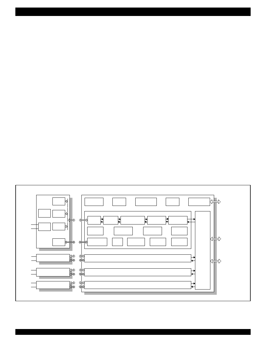
Figure - 1 Line Circuit Functions Included in the RSLIC-CODEC Chipset
Battery
Switch
Line
Driver
Filter
ADC
DAC
Programmable
Filters and Gain
PCM
Compander
Timeslot
Assignment
Off-hook
Detector
Ground Key
Detector
Ring
Generator
Ring Trip
Detector
Polarity
Reverse
ITDF
UTD
FSK
Generator
Tone
Generators
Ramp
Generator
PCM/GCI
Interface
Serial Control
Interface
SLIC Control
Interface
General
Control Logic
DSP
Core
Channel 1
Channel 2
RSLIC 2
#
CODEC
RSLIC 1
#
RSLIC 3
#
RSLIC 4
#
MPI Interface
PCM Interface
GCI Interface
Ring
Tip
Ring
Tip
Ring
Tip
Ring
Tip
Input
Stage
Logic
Control
Ring
Trip
Current
Sensor
Channel 3
Channel 4
Channel 2
17
RSLIC (IDT82V1671) & CODEC (IDT82V1074) CHIPSET INDUSTRIAL TEMPERATURE RANGE
3.2
DC FEEDING
3.2.1
DC FEEDING CHARACTERISTIC ZONES
Analog telephones require a DC current in the off-hook state with AC
voice signals in the transmit and receive directions superimposed. Thus,
once the telephone has gone off-hook, the SLIC must supply a DC
current to the subscriber line. The RSLIC-CODEC chipset provides a
fully programmable DC feeding characteristic to meet the requirements
of different applications.
The DC feeding characteristic has three different zones: the constant
current zone, the resistive zone and the constant voltage zone (see
Figure - 2
). A voltage reserve V
RES
is provided to avoid clipping the high
level AC signal.
3.2.2
CONSTANT CURRENT ZONE
In applications of short local loops, the DC feeding can be considered
as an ideal current source with an infinite internal resistance (R
I
), see
Figure - 3.
When the loop is in the off-hook state, the feeding current
usually must be kept at a constant level independent of the load. The
RSLIC senses the DC current and provides this information to CODEC
via the VTDC pin. The CODEC compares this value with the
programmed value and adjusts the RSLIC drivers as required.
Depending on the load, the operating point is determined by the
voltage V
Tip/Ring
between the Tip and Ring lines as follows:
V
Tip/Ring
= R
L
I
Tip/Ring
Where, R
L
represents the equivalent loop resistance. The lower the
load resistance R
L
, the lower the voltage V
Tip/Ring
.
When the DC feeding is operating in the constant current zone, the
indication bit FEED_I in register LREG21 will be set to 1, otherwise it is
set to 0.
3.2.3
RESISTIVE ZONE
The resistive zone is flexible in a wide range of applications,
especially applicable to medium line loops where the battery is unable to
feed a constant current to the line. In this zone, the DC feeding is
considered as a voltage source with a programmable internal resistance
(R
LIN
).
The operating point crosses from the constant current zone to the
resistive zone, as shown in
Figure - 4
.
When the DC feeding is operating in the resistive zone, the indication
bit FEED_R in register LREG21 will be set to 1, otherwise it is set to 0.
3.2.4
CONSTANT VOLTAGE ZONE
In very high impedance loops (long loops), the DC feeding can be
considered as a voltage source with zero internal resistance (R
V
).
In this zone, the voltage V
Tip/Ring
is constant and the current I
Tip/Ring
depends on the load between the Tip and Ring lines. See
Figure - 5
.
To avoid clipping the high level AC speech signals, a voltage reserve
V
RES
should be provided:
Where, V
BAT
is the selected battery voltage, V
LIM
is the open circuit
voltage.
Normally, V
RES
= 2 V.
When the DC feeding is operating at the constant voltage zone, the
indication bit FEED_V in register LREG21 will be set to 1, otherwise it is
set to 0.
Figure - 2 DC Feeding Zones
Figure - 3 Constant Current Zone
Resistive zone
Constant current zone
Constant voltage zone
V
TIP-RING
I
TIP-RING
Necessary Voltage Reserve V
RES
V
BAT
V
TIP-RING
I
TIP-RING
R
I
R
L
Figure - 4 Resistive Zone
V
TIP-RING
I
TIP-RING
R
LIN
R
L
V
RES
V
BAT
V
LIM
≠
=

18
RSLIC (IDT82V1671) & CODEC (IDT82V1074) CHIPSET INDUSTRIAL TEMPERATURE RANGE
3.2.5
DC FEEDING CHARACTERISTICS CONFIGURATION
The DC feeding characteristic is programmable. When the
DC_FEED bit in register LREG5 is set to 1, the default DC feeding
characteristic will be selected (see
Figure - 6
). The default configuration
is typically for -24 V battery voltage application. When the DC_FEED bit
is set to 0, the DC feeding characteristic is determined by the
coefficients written in the Coe-RAM.
IDT provides a software (Cal74) that can calculate the coefficients for
DC feeding. When users input the desired values for I
Max,
I
K1,
V
K1,
I
K2,
V
K2
and V
LIM,
Cal74 will automatically calculate the DC feeding
coefficients. When these coefficients are loaded to the Coe-RAM, the
DC feeding characteristic will meet the requirements.
To reduce power consumption and make the DC loop stable, it is
recommended to reduce I
MAX
and keep the output resistance (R
I
) less
than 5 k
when the loop is operated in the constant current zone.
Here is an example for short loop applications (see
Figure - 7
):
Loop resistance < 600
;
I
MAX
= 25 mA;
V
K1
= 20 V;
I
K1
= 20 mA (loop current requirement)
R
I
= |(V
K1
≠ 0)/(I
K1
≠ I
MAX
)| = |(20 ≠ 0)/(20 ≠ 25)| = 4 k
Figure - 5 Constant Voltage Zone
V
TIP-RING
I
TIP-RING
R
L
R
V
Figure - 6 DC Feeding Characteristics Configuration
Figure - 7 DC Feeding Configuration Example for Short Loop
Applications
V
TIP-RING
I
TIP-RING
I
Max
V
LIM
I
K1
I
K2
R
LIN
R
V
V
K2
V
K1
(25 mA)
(18 V, 23 mA)
(19.5 V, 16 mA)
(22 V)
V
TIP-RING
I
TIP-RING
14mA
40 48
36
I
MAX
(25 mA)
I
K1
(20 mA)
V
K1
(20 V)
R
I

19
RSLIC (IDT82V1671) & CODEC (IDT82V1074) CHIPSET INDUSTRIAL TEMPERATURE RANGE
Table - 1
lists the registers and the Coe-RAM locations used for DC
feeding configuration. For more information about the Coe-RAM, please
refer to
"5.2.5 Addressing the Coe-RAM" on page 61
and
Table - 23 on
page 62
.
Table - 1 Registers and Coe-RAM Locations Used for DC Feeding Configuration
Parameter
Register Bits/Coe-RAM Words
Notes
DC Feeding Coefficients Selection
Bit DC_FEED in LREG5
DC_FEED = 0: The DC feeding coefficient in the Coe-RAM is selected.
DC_FEED = 1: The DC feeding coefficient in the ROM is selected (default);
Constant current zone indication
Bit FEED_I in LREG21
When the DC feeding is operating at the constant current zone, the FEED_I bit is set to
1, otherwise it is set to 0.
Resistive zone indication
Bit FEED_R in LREG21
When the DC feeding is operating at the resistive zone, the FEED_R bit is set to 1,
otherwise it is set to 0.
Constant voltage zone indication
Bit FEED_V in LREG21
When the DC feeding is operating at the constant voltage zone, the FEED_V bit is set to
1, otherwise it is set to 0.
I
Max
DC Feeding Coefficients in the
Coe-RAM
Programmable via the Coe-RAM. Programmable range: 0 to 50 mA with
±
7% tolerance.
Default value (in the ROM): 25 mA.
I
K1
Programmable via the Coe-RAM. Programmable range: 0 to 50 mA with
±
7% tolerance.
Default value (in the ROM): 23 mA.
V
K1
Programmable via the Coe-RAM. Programmable range: 0 to 48 V with
±
7% tolerance.
The default value (in the ROM): 18 V.
I
K2
Programmable via the Coe-RAM. Programmable range: 0 to 50 mA with
±
7% tolerance.
Default value (in the ROM): 16 mA.
V
K2
Programmable via the Coe-RAM. Programmable range: 0 to 48 V with
±
7% tolerance.
Default value (in the ROM): 19.5 V.
V
LIM
Programmable via the Coe-RAM. Programmable range: 0 to 48 V with
±
7% tolerance.
Default value (in the ROM): 22 V.

20
RSLIC (IDT82V1671) & CODEC (IDT82V1074) CHIPSET INDUSTRIAL TEMPERATURE RANGE
3.3
SPEECH PROCESSING
3.3.1
AC TRANSMISSION
The signal paths for AC transmission between the RSLIC and the
CODEC is shown in
Figure - 8
. In the transmit direction, the transversal
and longitudinal currents on the subscriber line are sensed by the RSLIC
and the corresponding voltages are fed to the CODEC via VTAC and VL
pins. The voltage signals are further processed within the CODEC and
finally transmitted to the PCM highway. In the receive direction, the
CODEC processes data received from the PCM highway and outputs a
differential analog signal to the RSLIC via the ACP and ACN pins. The
RSLIC then amplifies this signal and applies it to the subscriber line.
3.3.1.1
Transmit Path
The voice signal path within the CODEC for one channel is shown in
Figure - 9
.
Figure - 8 Signal Paths for AC Transmission
VTAC
VL
ACP
ACN
RSLIC
#1
VTAC1
VL1
ACP1
ACN1
CODEC
PCM out
(Data Upstream)
PCM in
(Data Downstream)
Transmit
Receive
TIP
RING
VTAC
VL
ACP
ACN
RSLIC
#2
VTAC2
VL2
ACP2
ACN2
TIP
RING
VTAC
VL
ACP
ACN
RSLIC
#3
VTAC3
VL3
ACP3
ACN3
TIP
RING
VTAC
VL
ACP
ACN
RSLIC
#4
VTAC4
VL4
ACP4
ACN4
TIP
RING
MPI or GCI Interface
Transmit Path
Receive Path
Figure - 9 Voice Signal Path of the CODEC
Anti-Alias
Filter (AAF)
Sigma-Delta
Modulator
(SDM)
Digital Gain
Transmit
(GTX)
Low-Pass
Filter
Transmit
2nd
Decimation
Filter
Frequency Response
Correction Transmit
(FRX)
High-Pass
Filter Transmit
(HPF)
2nd
Interpolation
Filter
Digital Gain
Receive
(GRX)
3rd
Interpolation
Filter
Impedance
Matching
Filter (IMF)
Transhbrid
Balance Filter
(ECF)
1st
Interpolation
Filter
DX1/DX2
VTAC
ACP
ACN
1st
Decimation
Filter
PCM
Encoder
Frequency Response
Correction Receive
(FRR)
Low-Pass
Filter
Receive
Sigma-Delta
Demodulator
(D-SDM)
Smoothing
Filter & SCF
Gain for
Impedance
Scaling (GIS)
Analog Gain for
Impedance
Scaling (AGIS)
Programmable Filter
Fixed Filter
Receive Path
Transmit Path
Time Slot
Assignment
Time Slot
Assignment
DR1/DR2
PCM
Decoder
Analog Gain
Receive

21
RSLIC (IDT82V1671) & CODEC (IDT82V1074) CHIPSET INDUSTRIAL TEMPERATURE RANGE
In the transmit path, the analog voltage from the RSLIC is first filtered
by an anti-aliasing filter (AAF) and then is converted to a digital signal by
a 1-bit sigma-delta modulator (SDM). The digital signal is down-sampled
to an intermediate sample frequency to feed to the digital impedance
matching filter (IMF). Simultaneously, the down-sampled signal is
summed up with the output of the transhybrid balance filter (ECF). The
sum signal is transmitted through the transmit gain filter (GTX) and
further down-sampled to the baseband. A lowpass filter removes the
unwanted signals to meet ITU-T requirements and a frequency
response correction filter (FRX) follows to compensate for the
attenuation brought up by the impedance matching loop. The final stage
is a highpass filter (HPF) before the data is sent to the PCM encoder,
where data is A-law or µ-law compressed. At last, the data is assigned
to the selected time slot and transmitted to the PCM highway.
3.3.1.2
Receive Path
In the receive path, the signal received from the PCM highway is first
passed through the time slot assignment stage before being expanded
to a linear code at the baseband frequency of 8 kHz by the PCM
decoder. The expanded data is then up-sampled to a higher frequency
before passing through the frequency response correction filter (FRR)
that compensates for the attenuation brought up by the impedance
matching loop. The compensated signal is filtered by a lowpass filter and
further up-sampled to the intermediate frequency. The signal is then sent
to the receive gain filter (GRX). The output of the GRX goes in two ways:
one feeds to the transhybrid balance filter (ECF) and the other sums up
with the output of the digital impedance matching filter (IMF). This sum is
then up-sampled and processed by a digital sigma-delta demodulator
(D-SDM). An analog filter smooths the signal and outputs it to the RSLIC
via the ACP and ACN pins.
3.3.2
PROGRAMMABLE FILTERS
A comprehensive multi-rate signal process scheme with fixed/
programmable filters is applied to the AC loop of the RSLIC-CODEC
chipset to optimize the performance of the line card. In addition to fully
complying with the ITU-T G.712 specifications, the chipset also provides
additional programmable analog/digital filters to match impedance,
balance transhybrid, correct frequency response and adjust gains. All of
the coefficients of the digital filters can be calculated automatically by a
software (Cal74) provided by IDT. When these coefficients are written to
coefficient RAM, the final AC transmission characteristics of the line card
will meet ITU-T specifications.
Figure - 9
shows the programmable filters in the transmit and receive
paths.
3.3.2.1
Impedance Matching
For the RSLIC-CODEC chipset, impedance matching is realized with
three feedback loops in each channel: one analog loopback, the AGIS
(Analog Gain for Impedance Scaling) stage, and two digital loopbacks in
the programmable filters stage GIS (Gain for Impedance Scaling) and
IMF (Impedance Matching Filter). See
Figure - 9
for details. The analog
loopback realizes the real part value (Re Z
L
) of the impedance, while the
digital loopbacks realize the imaginary part value (Im Z
L
) of the
impedance. The GIS and IMF filter loops operate at 2 MHz and 64 kHz
rate respectively.
By programming the filters AGIS, GIS and IMF, the AC impedance of
the chipset can be set to any value inside the shadowed area in
Figure -
10
.
Figure - 10 Nyquist Diagram
0
300
-400
-600
600
900
1200
-200
Re Z
L
Im Z
L
Possible impedance values

22
RSLIC (IDT82V1671) & CODEC (IDT82V1074) CHIPSET INDUSTRIAL TEMPERATURE RANGE
The analog gain for impedance scaling (AGIS) can be 600
or 900
, as selected by the IM_629 bit in register LREG7. The option of
AGIS=600
is only applicable to loops with 600 equivalent
impedance, while the option of AGIS=900
is applicable to all loops
including those with 600
equivalent impedance. The AGIS value is set
to 600
by default.
The coefficient for the GIS filter is programmed by Gain for
Impedance Scaling in the Coe-RAM. It is programmable from
-128 to
+127 at increment of 1. The default value is 0.
If the IMF bit in LREG4 is set to 1, the IMF filter is disabled. If the IMF
bit is set to 0, the Impedance Matching Filter Coefficient in the Coe-RAM
is used by the IMF filter. Refer to
Table - 23 on page 62
for the
Coefficient RAM Mapping.
3.3.2.2
Transhybrid Balance
The RSLIC-CODEC chipset provides a traditional transhybrid
balance filter (ECF) for each channel to improve 4-wire return loss
performance. The ECF coefficient is programmable. If the ECF bit in
register LREG4 is set to 1, the ECF filter is disabled. If the ECF bit is set
to 0, the Transhybrid Balance Filter Coefficient in the Coe-RAM is used.
3.3.2.3
Frequency Response Correction
The frequency response correction filters are used to compensate for
the frequency distortion caused by the impedance matching filter. The
chipset provides two frequency response correction filters per channel:
one is in the transmit path (FRX), the other is in the receive path (FRR).
The FRX bit in LREG4 determines whether the FRX filter is disabled
or programmed by the Coe-RAM. If the FRX bit is set to 1, the FRX filter
is disabled. If the FRX bit is set to 0, the Coefficient for Frequency
Response Correction in the Transmit Path in the Coe-RAM is used.
The FRR bit in LREG4 determines whether the FRR filter is disabled
or programmed by the Coe-RAM. If the FRR bit is set to 1, the FRR filter
is disabled. If the FRR bit is set to 0, the Coefficient for Frequency
Response Correction in the Receive Path in the Coe-RAM is used.
3.3.2.4
Gain Adjustment
For each channel, the gain in the transmit path is adjusted by
programming the digital filter GTX. The transmit gain can be up to +12
dB in minimum steps of 0.05 dB. If the GTX bit in LREG4 is set to 1, the
default transmit gain of 0 dB is selected. If the GTX bit is set to 0, the
transmit gain is programmed via the Coe-RAM.
For each channel, the gain in the receive path consists of analog
gain and digital gain (GRX). The analog gain is fixed at 0 dB. The digital
gain is programmable from
-12 dB to +3 dB in minimum steps of 0.05
dB. If the GRX bit in LREG4 is set to 1, the digital gain in the receive
path will be 0 dB (default value), otherwise, it is programmed via the
Coe-RAM.
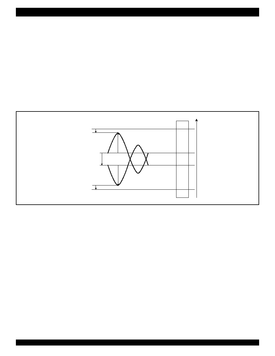
23
RSLIC (IDT82V1671) & CODEC (IDT82V1074) CHIPSET INDUSTRIAL TEMPERATURE RANGE
3.4
RING AND RING TRIP
The RSLIC-CODEC chipset supports both internal and external
ringing modes to meet different requirements.
3.4.1
INTERNAL RINGING MODE
3.4.1.1
Internal Ringing Generation
The chipset provides a built-in ring generator per channel that can
generate balanced sinusoidal ringing signal without external
components. The frequency, amplitude and DC offset of the ringing
signal are programmable. In addition, the ring trip detection can be
performed internally by programming the ring trip threshold.
If internal ringing mode is selected, the RSLIC will be automatically
switched to the higher battery (VBH) for ringing generation. The ringing
signal generated by the CODEC is sent to the RSLIC via the DCP and
DCN pins and further fed to the subscriber line by the RSLIC. Refer to
Figure - 49 on page 104
for an application circuit using internal ringing.
To generate a ringing signal, users should first set the operating
mode to Internal Ringing (the CODEC is set to the RING mode and the
RSLIC is set to Internal Ringing mode, refer to
Table - 3
for details).
Next, calculate the coefficients of the ringing frequency, amplitude and
DC offset and load the coefficients to the Coe-RAM (the calculation is
performed by a software (Cal74) provided by IDT. When users input the
frequency, amplitude and offset values, Cal74 will calculate the
coefficients automatically). Then, the ringing generation will be
controlled by the RING_EN bit in LREG7. In order to reduce noise and
crosstalk on adjacent lines, the ringing signal will automatically start at a
zero-crossing after the RING_EN bit is set to 1 and stop at zero-crossing
after the RING_EN bit is set to 0.
Figure - 11
shows a balanced ringing signal generated by the
chipset.
3.4.1.2
Ring Trip Detection In Internal Ringing Mode
Once the subscriber has switched from on-hook state to off-hook
state during ringing, the ringing signal must be removed from the
subscriber line before normal speech begins. The recognition of an off-
hook state during ringing, together with the removal of the ringing signal,
is commonly referred to as ring trip. Depending on the application
requirements, the RSLIC-CODEC chipset offers two different ring trip
methods for internal ringing mode, they are DC ring trip detection and
AC ring trip detection, as selected by the RT_SEL bit in LREG7.
∑ DC Ring Trip Detection
Most applications use DC ring trip detection. By applying a DC offset
voltage together with the ringing signal, a transversal DC loop current
starts to flow when the subscriber goes off-hook. The RSLIC senses the
DC current and supplies the corresponding sensed voltage to the
CODEC via the VTAC pin. The CODEC continuously integrates this
voltage over one ringing period without rectifying. The result represents
the DC component of the ring current. If the DC component exceeds the
programmed DC ring trip threshold, the corresponding HK[n] bit (n = 0 to
3 are for Channel 1 to 4 respectively) in register GREG26 will be set to 1
to indicate that the loop has been off-hook. An interrupt will be generated
simultaneously if the corresponding mask bit HK_M[n] is set to 0.
Most of the applications use DC ring trip detection because it is very
reliable. Even with very long and noisy lines the off-hook condition can
reliably be detected within two ringing period by the DC ring trip. The DC
ring trip method is selected by setting the RT_SEL bit in LREG7 to 1.
The DC offset voltage is programmed by the RingOffset in the coefficient
RAM. See
Table - 2
for detailed information.
In DC ring trip mode, when an off-hook event is detected, the ringing
signal will stop immediately at zero-crossing. But the RING_EN bit will
not be cleared to 0 automatically; it should eventually be cleared by
software. This automatic ring trip function speeds up the response to off-
hook for time critical applications.
∑ AC Ring Trip Detection
For short loop applications, the DC offset can be removed from the
ringing signal to increase the achievable voltage amplitude for a given
supply voltage. The AC ring trip detection without DC offset is realized
by rectifying sensed ring current signal, integrating it over one ringing
signal period and comparing the result with the programmed AC ring trip
threshold. If the threshold is exceeded, the corresponding bit HK[n] (n =
0 to 3 are for Channel 1 to 4 respectively) in register GREG26 will be set
Figure - 11 Internal Balanced Ringing
V
DROP.T
V
DC.RING
V
DROP.R
V
Tp
V
Rp
V
T
V
R
V
RING.PP
= V
Tp
- V
Rp
BGND
VBH
RSLIC
Tip Line
Ring Line
24
RSLIC (IDT82V1671) & CODEC (IDT82V1074) CHIPSET INDUSTRIAL TEMPERATURE RANGE
to 1 to indicate off-hook detected. An interrupt will be generated if the
HK[n] bit is not masked.
Note that during a ring pause period, the off-hook condition can not
be detected by the AC ring trip. When the off-hook condition is detected
during a ring burst period, the ringing signal will be removed
automatically at zero-crossing. As the RING_EN bit remains unchanged,
users should clear it to 0 by software.
If several telephones are in parallel with each other between the Tip
and Ring lines, the on-hook AC current will increase. If the AC load is
too large, the on-hook current of short loop will be larger than the off-
hook current of long loop - this will possibly cause a false indication of
the off-hook condition. Consequently, the AC ring trip detection method
should only be used in short loops (loop impedance < 1 k
) and low-
power applications.
Table - 2
lists the programmable parameters used for internal ringing
generation and ring trip detection.
3.4.2
EXTERNAL RINGING MODE
The chipset can generate internal ringing signals of up to 70 Vp. In
applications of requiring higher ring amplitudes, external ringing signals
can be used.
Figure - 50 on page 105
shows an application circuit that
use an external ringing signal.
If the RSLIC is set to External Ringing mode (see
Table - 3
for
details), the ringing signal from an external ring generator will be
switched to the Tip/Ring lines through an external relay during ring burst
period, and will be removed during ring pause period.
The CODEC provides two programmable IO pins (IO1 and IO2) with
relay-driving capability for each channel. They can be used to control the
external ring relay without additional components. The external ringing
can be switched on/off in two different modes as described below:
∑ Synchronous mode (this mode is available when the IO1 pin is
selected to control the external ring relay). In this mode, the external
ringer provides a synchronous signal for the CODEC via the RSYNC pin
to ensure switching the ringing signal at zero-crossing. This
synchronous mode is enabled by setting the SYNC_EN bit in LREG19 to
1. When the IO1 pin of the CODEC is configured as an output (LREG20:
IO_C[0] = 1), the external ringing signal will be switched on the RSYNC
edge (rising or falling) next to the change of the IO1 pin, as illustrated in
Figure - 12
.
The logic level of the IO1 pin is set by the IO[0] bit in
LREG20:
IO[0] = 0: IO1 pin is set to logic low;
IO[0] = 1: IO1 pin is set logic high.
In synchronous mode, the CODEC provides a hardware ring trip
function to speed up the response of off-hook event. For example, if a
logic low on the IO1 pin starts the ringing while a logic high on this pin
stops the ringing, once an off-hook event is detected during ring burst
period, the IO1 pin will be set to logic high automatically to remove the
ringing signal although the IO[0] bit remains 0. Users should set the
IO[0] bit to 1 by software.
∑ Asynchronous mode. If no synchronous signal is applied to the
RSYNC pin of the CODEC, or some applications need to switch the
ringing signal without any delay caused by zero-crossing
synchronization, the SYNC_EN bit in LREG19 should be set to 0. In this
case, the external ringing signal will be switched immediately after the
corresponding IO pin control bit (IO[0] for the IO1 pin and IO[1] for the
Table - 2 Registers and Coe-RAM Locations Used for Internal Ringing Mode
Parameter
Register Bits/Coe-RAM Words
Notes
Internal Ringing Mode Selection
MPI mode: bit RING in LREG7, bits
SCAN_EN and SM[2:0] in LREG6;
GCI mode: bit RING in LREG7, bits
SCAN_EN and SM[2:0] in downstream C/I
channel byte.
RING = 1: the CODEC is set to Ring mode
SCAN_EN = 1 and SM[2:0] = 010: the RLSIC is set to Internal Ringing mode.
Internal Ringing Enable
Bit RING_EN in LREG7
RING_EN = 0: ring pause;
RING_EN = 1: ring burst.
Internal Ringing Parameters
Selection
Bit RG in LREG5
RG = 0: ringing parameters in the Coe-RAM are selected.
RG = 1: ringing parameters (frequency, amplitude and offset) in the ROM are
selected (default);
Internal Ringing Frequency
Word RingFreq in the Coe-RAM
Programmable via the Coe-RAM. Programmable range: 20 to 200 Hz with
±
3%
tolerance. Default value (in the ROM): 30 Hz.
Internal Ringing Amplitude
Word RingAmp in the Coe-RAM
Programmable via the Coe-RAM. Programmable range: 0 to 70 Vp with
±
1%
tolerance. Default value (in the ROM): 40 Vp.
Internal Ringing Offset Voltage
Word RingOffset in the Coe-RAM
Programmable via the Coe-RAM. Programmable range: 0 to 20 V with
±
1%
tolerance. Default value (in the ROM): 7 V.
Ring Trip Method Selection
Bit RT_SEL in LREG7
RT_SEL = 0: AC ring trip is selected;
RT_SEL = 1: DC ring trip is selected.
Ring Trip Threshold Selection
Bit Signaling in LREG5
Signaling = 0: The AC and DC ring trip thresholds in the Coe-RAM are selected;
Signaling = 1: The AC and DC ring trip thresholds in the ROM are selected (default);
AC Ring Trip Threshold
Word RTthld_AC in the Coe-RAM
Programmable via the Coe-RAM. Programmable range: 0 to 20 mA with
±
5%
tolerance. Default value (in the ROM): 5 mA.
DC Ring Trip Threshold
Word RTthld_DC in the Coe-RAM
Programmable via the Coe-RAM. Programmable range: 0 to 20 mA with
±
5%
tolerance. Default value (in the ROM): 5 mA.
Ring Trip Detection Result
Indication
Bits HK[n] in GREG26
Indicating the ring trip detection result, `0' means Channel n+1 is on-hook while `1'
means Channel n+1 is off-hook (n = 0 to 3)

25
RSLIC (IDT82V1671) & CODEC (IDT82V1074) CHIPSET INDUSTRIAL TEMPERATURE RANGE
IO2 pin) in LREG20 is changed, irrespective of whether the ringing
signal is at a zero-crossing or not. In this mode, even if the IO1 pin is
used to control the ring relay, it will act as a normal IO pin. In other
words, the hardware ring trip function is no longer available and the IO1
pin is controlled completely by software through the CODEC.
3.4.2.1
Ring Trip Detection In External Ringing Mode
In external ringing mode, the sensed ring current signal is processed
by an operational amplifier in the RSLIC and supplied to the CODEC via
the RTIN pin for ring trip detection. In external ringing mode, the level
meter will be involved when detecting the ring trip. For detailed
information about the level meter, please refer to
"3.9.4 Level Meter" on
page 40
.
To detect ring trip, the steps below should be followed:
1. Select the RTIN as the input source to the DC path (LREG9:
LM_SEL[3:0] = 1100);
2. Write the external ring trip threshold to HKthld in the Coe-RAM;
3. Set the CODEC to ACTIVE mode and set the RSLIC to External
Ringing mode (the chipset operating mode control bits are
different in MPI interface and GCI interface, refer to
Table - 3
for
details);
4. The CODEC processes the RTIN signal and compares the result
with the external ring trip threshold written in HKthld in the Coe-
RAM. If the threshold is exceeded, the corresponding HK[n] bit in
GREG26 (n = 0 to 3 corresponds to Channel 1 to 4) will be set to
1, indicating that off-hook is detected.
When detecting a ring trip, an offset voltage (about 10 to 30 mV) may
be introduced by the operational amplifier mentioned above. This offset
can be measured by the DC level meter and compensated by writing the
corresponding compensation value to DC Offset in the Coe-RAM.
Before measuring this offset voltage, make sure that no external
ringing signal is applied to the Tip/Ring lines. The measuring procedure
is as follows (to understand the following descriptions, users should
understand the level meter first):
1. Set the CODEC to ACTIVE mode and set the RSLIC to External
Ringing mode (see
Table - 3
for details);
2. Select the RTIN as the input to the DC path of the CODEC
(LREG9: LM_SEL[3:0] = 1100);
3. In LREG8, set DC_SRC = 1 and LM_SRC = 0;
4. Select the channel to be measured by setting the LM_CS[1:0] bits
in GREG16 accordingly;
5. Set the integrating time to 001H (GREG15 & GREG16:
LM_CN[10:0] = 001H);
6. Set the shift factor (K[3:0] in LREG9);
Figure - 12 External Ringing Synchronization
External Ringing Voltage
V
RSYNC
V
IO 1
V
RING
t
t
t
t
IO [0] bit in LREG 20
t
Suppose a logic low on the
IO 1 pin starts the ringing.

26
RSLIC (IDT82V1671) & CODEC (IDT82V1074) CHIPSET INDUSTRIAL TEMPERATURE RANGE
7. Disable the rectifier (LREG10: LM_RECT = 0);
8. Set the gain factor as required (LREG10: LM_GF);
9. Set the level meter measurement mode to ONCE and start the
measurement (GREG16: LM_ONCE = 1, LM_EN = 1);
10.Read the measurement result from GREG17 & GREG18 (16-bit);
11. Right shift the 16-bit result for two bits, then the result is the offset
value in the form of a 14-bit two's complement;
12.Invert each bit of the offset value and add 1 to it, write this result to
DC Offset in the Coe-RAM.
13.Select this offset compensation value to be used (LREG4:
DC_OFT = 0);
14.Restore the modified registers with original contents;
Then, the four steps mentioned above follow and off-hook event will
be more reliably detected.
Table - 3
shows the registers and Coe-RAM locations used for
external ringing mode.
Table - 3 Registers and Coe-RAM Locations Used for External Ringing Mode
Parameter
Register Bits
Notes
CODEC and RSLIC Operating Mode
Configuration
MPI mode: bits ACTIVE, SCAN_EN and SM[2:0]
in LREG6;
GCI mode: bit ACTIVE in LREG6, bits SCAN_EN
and SM[2:0] in downstream C/I channel byte.
ACTIVE = 1: the CODEC is set to Active mode
SCAN_EN = 1 and SM[2:0] = 001: the RLSIC is set to External Ringing
mode.
External Ring Relay Control
(recommended)
Bit IO_C[0] in LREG20
Bit IO[0] in LREG20
IO_C[0] = 1: the IO1 pin is configured as an output
IO[0] = 0: the IO1 pin is set to logic low
IO[0] = 1: the IO1 pin is set to logic high
Synchronous Mode Enable Bit
Bit SYNC_EN in LREG19
SYNC_EN = 0: asynchronous mode is selected
SYNC_EN = 1: synchronous mode is selected
External Ring Trip Detection Source Bit LM_SEL[3:0] in LREG9
LM_SEL[3:0] = 1100: RTIN is selected to the DC path for ring trip detection
External Ring Trip Threshold
Word HKthld in the Coe-RAM
If the Signaling bit in LREG5 is set to 1, the external ring trip threshold in
the ROM is selected, otherwise the threshold written in HKthld in the Coe-
RAM is selected.
The HKthld in the Coe-RAM is programmable from 0 to 20 mA with
±
5%
tolerance. The default value (in the ROM) is 7 mA.
Note that both the off-hook detection threshold in active mode and the
external ring trip threshold are written in HKthld in the Coe-RAM. Users
should change the threshold according to different conditions.
External Ring Trip Detection Result
Indication
Bits HK[n] in GREG26
Indicating the ring trip detection result, `0' means Channel n+1 is on-hook
while `1' means Channel n+1 is off-hook (n = 0 to 3).
Level Meter Configuration and Result
Registers
LREG8: LM_SRC, DC_SRC
LREG9: K[3:0]
LREG10: LM_GF, LM_RECT
GREG15 & GREG16
GREG17 & GREG18
Refer to
Table - 17 on page 44
for details.
DC Offset Compensation
Bit DC_OFT in LREG4
Word DC Offset in the Coe-RAM
DC_OFT = 0: compensation value in word DC Offset in the Coe-RAM is
selected;
DC_OFT = 1: compensation value (which is 0) in the ROM is selected
(default).

27
RSLIC (IDT82V1671) & CODEC (IDT82V1074) CHIPSET INDUSTRIAL TEMPERATURE RANGE
3.5
SUPERVISION
Supervision is performed internally by the RSLIC-CODEC chipset.
The RSLIC senses the longitudinal and transversal line currents on the
Ring and Tip lines, and feeds the corresponding voltages to the CODEC
via the VL, VTAC and VTDC pins for further process. In this way, the
signaling in the subscriber loop is monitored.
3.5.1
OFF-HOOK DETECTION
Loop start signaling is the most common type of signaling. The
subscriber loop is closed by the hook switch inside the subscriber
equipment. For the RSLIC-CODEC chipset, the off-hook detection can
be operated in two different modes as shown in
Table - 4
.
∑ Active mode
In this mode, both the RSLIC and the CODEC are active. The RSLIC
senses the transversal current on the Ring and Tip lines, and feeds the
corresponding voltage to the CODEC via VTDC pin. Inside the CODEC,
this voltage is A-to-D converted and filtered. The result is compared with
the programmed off-hook threshold (word HKthld in the Coe-RAM). If
the result exceeds the threshold, the bit HK[n] (n = 0, 1, 2 or 3) in
register GREG26 will be set to 1, indicating that Channel n+1 is off-hook.
An interrupt will be generated at the same time if the off-hook mask bit
HK_M in register LREG18 is disabled (`0').
In active mode, to detect the loop transition from off-hook to on-hook,
the on-hook threshold should be used. The off-hook threshold minus a
programmable hysteresis value is the on-hook threshold (as shown in
Figure - 13
). The hysteresis value is programmed by HKHyst in the Coe-
RAM. The default value is 2 mA.
∑ Sleep mode
In this mode, both the CODEC and the RSLIC are in standby mode.
All of the function blocks except off-hook detection stop working. The
transversal current on the Ring and Tip lines is sensed by a simple
sense circuit and the corresponding sensed voltage is fed to an analog
comparator in the CODEC via the VTAC pin. By comparing this sensed
voltage with a fixed off-hook threshold of 2 mA, the off-hook event can
be detected. Once the loop goes off-hook, the whole chipset should be
set to active mode by the master processor.
The CODEC integrates a programmable debounce filter in the off-
hook detection circuit to eliminate disturbance. The transversal DC
signal (which is taken as the off-hook criterion) will be filtered by this
debounce filter. The DC signal with duration less than the debounce time
will be ignored. As shown in
Figure - 14
, a four-bit debounce counter
allows the debounce interval programmable from 0.125 ms to 2 ms. A
16-state up/down counter follows, resulting in the minimal debounce
time ranging from 2 ms to 32 ms. The debounce interval is programmed
by the DB[3:0] bits in LREG11.
(Note: When the RSLIC operating mode is switching from other
mode to the active mode, there might be a narrow pulse of about 15 ms
occurring on VTDC, resulting in a false off-hook interrupt to be
generated. If this happens, please set the debounce time for off-hook
detection to 15 ms or above (i.e., DB[3:0]
0111B) to filter the noise
pulse.)
Table - 5
shows the registers and Coe-RAM locations used for off-
hook detection.
Table - 4 Off-hook Detection in Different Modes
Chipset Mode
CODEC Mode
RSLIC Mode
Mode Control Register Setting
Active
Active
Active
MPI mode: LREG6: ACTIVE = 1, SCAN_EN = 1, SM[2:0] = 000
GCI mode: LREG6: ACTIVE = 1; downstream C/I channel byte: SCAN_EN = 1, SM[2:0] = 000
Sleep
Standby
Standby
MPI mode: LREG6: STANDBY = 1, SCAN_EN = 1, SM[2:0] = 110
GCI mode: LREG6: STANDBY = 1; downstream C/I channel byte: SCAN_EN = 1, SM[2:0] = 110
Note: The operating mode of the CODEC is set by register LREG6. The operating mode of the RSLIC is set by register LREG6 (for MPI mode) or downstream C/I
channel byte. Refer to
"6.1 Operating Modes" on page 87
for further details.
Figure - 13 Hysteresis for Off-Hook Detection
I
Hook State
Indication
Off-hook
Threshold
On-hook
Threshold
Hysteresis
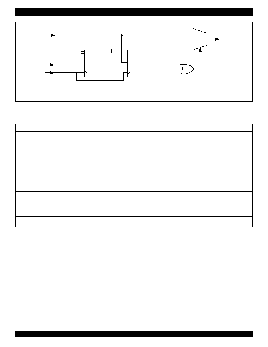
28
RSLIC (IDT82V1671) & CODEC (IDT82V1074) CHIPSET INDUSTRIAL TEMPERATURE RANGE
Figure - 14 Debounce Filter for Off-hook/Ground-key Detection
Table - 5 Registers and Coe-RAM Locations Used for Off-hook Detection
Parameter
Register Bits/Coe-RAM Words
Notes
Off-hook Indication
Bits HK[3:0] in GREG26
HK[n] = 0: Channel n+1 is on-hook (n = 0 to 3);
HK[n] = 1: Channel n+1 is off-hook.
Mask bit for HK[3:0] bits
Bit HK_M in LREG18
HK_M = 0: each change of HK[3:0] bits generates an interrupt;
HK_M = 1: changes of HK[3:0] bits do not generate interrupts.
Off-hook Threshold Selection
Bit Signaling in LREG5
Signaling = 0: the off-hook threshold in the Coe-RAM is selected.
Signaling = 1: the off-hook threshold in the ROM is selected (default).
Off-hook Threshold for Active Mode
Word HKthld in the Coe-RAM
If the Signaling bit in LREG5 is set to 0, the off-hook threshold for active mode is
programmed by word HKthld in the Coe-RAM. It is programmable from 0 to 20 mA with
±
5% tolerance.
If the Signaling bit in LREG5 is set to 1, the default value of 7 mA (stored in the ROM) is
selected.
Hysteresis for Off-hook Detection
Word HKHyst in the Coe-RAM
If the Signaling bit in LREG5 is set to 0, the hysteresis for off-hook detection is
programmed by word HKhyst in the Coe-RAM. It is programmable from 0 to 20 mA with
±
5% tolerance.
If the Signaling bit in LREG5 is set to 1, the default value of 2 mA (stored in the ROM) is
selected.
Debounce Interval Selection
Bits DB[3:0] in LREG11
The interval is programmable from 0.125 ms to 2 ms in steps of 0.125 ms. The default
value of DB[3:0] is `0000', corresponding to the minimum debounce interval of 0.125 ms.
Q
DB[3:0]
Debounce Interval
(0.125 ms
- 2 ms)
Up/down
Q
16 states
Up/down Counter
4 bit Debounce
Counter
0
1
Off-hook/
Ground-key
D
En
FS
MCLK
En
MUX
DB[0]
DB[1]
DB[2]
DB[3]
Debounced
Off-hook/
Ground-key
29
RSLIC (IDT82V1671) & CODEC (IDT82V1074) CHIPSET INDUSTRIAL TEMPERATURE RANGE
3.5.2
GROUND-KEY DETECTION
In applications of using ground-key signaling, the longitudinal current
of the loop is used as ground-key criterion. The RSLIC senses the
longitudinal current and transfers the scaled longitudinal voltage
information to the CODEC via VL pin. An analog comparator for ground-
key detection compares this voltage with a fixed threshold (11.8 mA). If
the threshold is exceeded, the bit GK[n] (n = 0, 1, 2 or 3) in register
GREG26 will be set to 1 to indicate that ground-key is detected in
Channel n+1. An interrupt will occur if any bit of GK[3:0] changing from 0
to 1. The GK[3:0] bits can be masked by the GK_M bit in register
LREG18.
The polarity of the longitudinal current is indicated by the GK_POL bit
in register LREG21. Each change of the GK_POL bit generates an
interrupt. The GK_POL bit can be masked by the GKP_M bit in register
LREG18.
An application example is shown in the following:
∑ Tip open or Ring open mode
In this case, the Tip line or the Ring line is switched to high
impedance, the longitudinal current on the Ring or Tip line is sensed by
the RSLIC and fed to the CODEC through the VL pin for testing.
The longitudinal DC signal (which is taken as the ground-key
criterion) is also filtered by the programmable debounce filter used in off-
hook detection. The DC signal with duration less than the denounce time
will be ignored. The debounce interval is programmable by the DB[3:0]
bits in register LREG11. Refer to
Figure - 14
for details.
Table - 6
shows the registers used for ground-key detection.
3.6
METERING BY POLARITY REVERSAL
The RSLIC-CODEC supports metering by reversing the polarity of
the voltage on the Tip and Ring lines. The actual polarity of this voltage
is reversed by setting the REV_POL bit in register LREG19 to 1.
The voltage polarity is reversed in a smooth way to avoid generating
non-required ringing. Users can control the transition time (time from
start to end of polarity reversal) by programming the built-in ramp
generator. Refer to
"Ramp Generator" on page 47
for further details.
Table - 6 Registers Used for Ground-key Detection
Parameter
Register Bits
Notes
Ground-key Indication
Bits GK[3:0] in GREG26
GK[n] = 0: no longitudinal current detected in Channel n+1 (n = 0 to 3);
GK[n] = 1: longitudinal current detected in Channel n+1.
Mask bit for GK[3:0] bits
Bit GK_M in LREG18
GK_M = 0: each change of the GK[3:0] bits generates an interrupt;
GK_M = 1: changes of the GK[3:0] bit do not generate interrupts.
Ground-key Polarity
Bit GK_P in LREG21
GK_P = 0: negative ground-key threshold level active;
GK_P = 1: positive ground-key threshold level active.
Mask bit for GK_P bit
Bit GKP_M in LREG18
GKP_M = 0: each change of the GK_P bit generates an interrupt;
GKP_M = 1: changes of the GK_P bit do not generate interrupt.
Debounce Interval Selection
Bits DB[3:0] in LREG11
The interval is programmable from 0.125 ms to 2 ms in steps of 0.125 ms.

30
RSLIC (IDT82V1671) & CODEC (IDT82V1074) CHIPSET INDUSTRIAL TEMPERATURE RANGE
3.7
ENHANCED SIGNAL PROCESSING
Besides the fundamental BORSCHT functions, the RSLIC-CODEC
chipset also provides several additional functions such as Tone
Generation, FSK generation for Caller-ID and Universal Tone Detection.
These additional functions can be individually enabled or disabled
according to the requirements of applications.
3.7.1
TONE GENERATOR
The CODEC provides two tone generators for each channel: Tone
Generator 1 (TG1) and Tone Generator 2 (TG2). They can be used to
generate signals such as a test tone, DTMF, dial tone, busy tone,
congestion tone and Caller-ID alerting tone etc., and output them to the
RSLIC via the ACP and ACN pins.
The TG1 and TG2 of each channel can be enabled by setting bits
TG1_EN and TG2_EN in register LREG7 to 1, respectively.
If the TG bit in register LREG4 is set to 1, the default frequency and
amplitude values in the ROM are selected for tone generators (default:
TG1Amp = 0.94 V, TG1Freq = 852 Hz, TG2Amp = 0.94 V, TG2Freq =
1447 Hz). Otherwise, the frequency and amplitude values of TG1 and
TG2 are programmed by the Coe-RAM. The frequency and amplitude
coefficients can be calculated, respectively, by the following formulas:
f<2000 Hz, Frequency coefficient = 8191
cos(f/80002)
f>2000 Hz, Frequency coefficient = 16384 - 8191
cos(f/80002)
Amplitude coefficient = A
8191sin(f/80002)
Herein, 'f' is the desired frequency of the tone. 'A' is the scaling
parameter for the tone amplitude. The range of 'A' is from 0 to 1.
A = 1, corresponding to the maximum amplitude, 1.57 (V);
A = 0, corresponding to minimum amplitude, 0 (V).
It is a linear relationship between 'A' and the amplitude, which means
if A =
(0< < 1), the amplitude will be 1.57 (V).
The frequency is programmable from 25 Hz to 3400 Hz. The
tolerance is as follows
:
f < 200 Hz, tolerance <
± 3%;
f > 200 Hz, tolerance <
± 1.5%.
The amplitude and frequency coefficients of the tone signal can be
calculated by the Cal74 software automatically. Refer to
Table - 7
for
more information about registers and Coe-RAM used for tone
generators.
Note that when using the dual tone generators, users must write
2000H (high byte: 20H; low byte: 00H) to block2 word4 of the Coe-
RAM to ensure proper operation.
3.7.1.1
DTMF Generation
Dual Tone Multi-Frequency (DTMF) is a signaling scheme using
voice frequency tones to signal dialing information. A DTMF signal is the
sum of two tones, one from the low frequency group (697 - 941 Hz) and
one from the high frequency group (1209 - 1633 Hz), with each group
containing four individual tones. This scheme allows 16 unique
combinations. Ten of these codes represent the numbers from zero
through nine on the telephone keypad, the rest six codes (
, #, A, B, C,
D) are reserved for special signaling. The buttons are arranged in a
matrix, with the rows determining the low group tones, and the columns
determining the high group tone for each button.
Based on the scheme described in the preceding paragraph, a
DTMF signal can be generated by the two tone generators. By
programming the amplitude and frequency of the tone generators
through MPI or GCI interface, the 16 standard DTMF pairs can be
generated independently in each channel. The generated DTMF tone
signals meet the frequency variation tolerances specified in the ITU-T
Q.23 recommendation.
3.7.2
FSK GENERATION FOR CALLER ID
The RSLIC-CODEC chipset provides an optimized FSK generator for
sending Caller ID information. Different countries use different standards
to send Caller ID information by FSK codes. The FSK modulation of the
RSLIC-CODEC chipset is compatible with the most common standards:
BELL 202 and ITU-T V.23.
Table - 8
shows the modulation
characteristics of these two standards.
Table - 7 Registers and Coe-RAM Locations Used for Tone Generation
Parameter
Register Bits/Coe-RAM Words
Notes
TG Frequency and Amplitude
Coefficients Selection
Bit TG in LREG4
TG = 0: The frequency and amplitude coefficients in the Coe-RAM are selected for the tone
generators;
TG = 1: The frequency and amplitude coefficients in the ROM are selected for the tone
generators (default);
TG1 Enable/Disable Bit
Bit TG1_EN in LREG7
TG1_EN = 0: TG1 is disabled.
TG1_EN = 1: TG1 is enabled.
TG1 Amplitude Coefficient
Word TG1Amp in the Coe-RAM
The amplitude is programmable from 0 V to 1.57 V with
±
1% tolerance. The default amplitude
(in the ROM) is 0.94 V.
TG1 Frequency Coefficient
Word TG1Freq in the Coe-RAM
The frequency is programmable from 25 to 3400 Hz. The tolerance is
±
3% (f<200 Hz) or
±
1.5% (f>200 Hz). The default frequency (in the ROM) is 852 Hz.
TG2 Enable/Disable Bit
Bit TG2_EN in LREG7
TG2_EN = 0: TG2 is disabled
TG2_EN = 1: TG2 is enabled
TG2 Amplitude Coefficient
Word TG2Amp in the Coe-RAM
The amplitude is programmable from 0 V to 1.57 V with
±
1% tolerance. The default amplitude
(in the ROM) is 0.94 V.
TG2 Frequency Coefficient
Word TG2Freq in the Coe-RAM
The frequency is programmable from 25 to 3400 Hz. The tolerance is
±
3% (f<200 Hz) or
±
1.5% (f>200 Hz). The default frequency (in the ROM) is 1447 Hz.
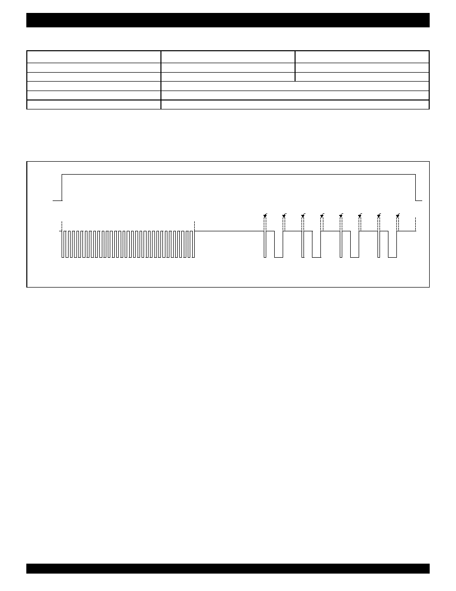
31
RSLIC (IDT82V1671) & CODEC (IDT82V1074) CHIPSET INDUSTRIAL TEMPERATURE RANGE
Generally, the transmission of the FSK signal starts with a Seizure
Signal, which is a string of '01' pairs. Then a Mark Signal which is a
string of `1' follows. The Caller ID information comes after the Mark
Signal. Between two bytes of the Caller ID information, a Flag Signal
which is a string of '1' is inserted so that the receiver can have enough
time to process the received bytes. The transmission sequence of the
FSK signal is shown in
Figure - 15
.
The lengths of the Seizure Signal, Mark Signal, Flag Signal and
Caller ID data are programmable by register GREG21, GREG22,
GREG19 and GREG20, respectively.
The CODEC provides total 64 bytes RAM (called FSK-RAM) to store
the Caller ID information. If the length of the information is less than 64
bytes, all information bytes can be written to the FSK-RAM at one time.
If the length of the information is longer than 64 bytes, the information
should be divided into two or more segments according to its actual
length (each segment
64 bytes). Write one segment to the FSK-RAM
at one time. When this segment has been sent out, the FSK-RAM can
be updated with the next segment. Repeat the same operation until all
segments have been sent out. Refer to
"5.2.4 Addressing the FSK-
RAM" on page 60
for further details on accessing the FSK-RAM via MPI
or GCI interface.
The FSK generator is controlled by register GREG23, as described
in the following:
- Bit FSK_EN. This bit is used to enable or disable the FSK
generator. The FSK_EN bit must be set to 1 to enable the FSK
generator before FSK transmission starts. When the transmission is
finished, the FSK_EN bit should be set to 0 to disable the FSK
generator.
- Bits FSK_CS[1:0]. These two bits are used to select a channel to
send FSK signal (the FSK generator is shared by four channels).
- Bit FSK_BS. This bit is used to select one of the two FSK
modulation standards BELL 202 and ITU-T V.23.
- Bit FSK_TS. This bit is used to start the FSK transmission. Once
the FSK_TS bit is set to 1, the FSK generator begins to send the data
written in the FSK-RAM automatically, following the procedure shown
below:
Step 1: Start, send Seizure Signal;
Step 2: Send Mark Signal;
Step 3: Send one start bit (0), one byte of data in the FSK-RAM,
one stop bit (1), then send Flag Signal;
Step 4: Check whether all data in the FSK-RAM has been sent out.
If it has, set the FSK_TS bit to 0 and stop, otherwise return
to step 3.
- Bit FSK_MAS. This bit determines whether the FSK generator will
output a mark-after-send signal (a string of `1') after the data in the FSK-
RAM has been sent out. If total Caller ID information is longer than 64
bytes, the FSK_MAS bit should be set to 1. After sending out one
segment, the FSK generator will keep sending out a mark-after-send
signal to hold the established communication channel for sending the
remaining segment(s). After all segments have been sent out, the
FSK_MAS bit should be set to 0 so that the output of the FSK generator
will be muted. Once the FSK_MAS bit is 0, changing it from 0 to 1 will
not make the mark-after-send signal active until a new transmission
starts (FSK_TS = 1).
If total Caller ID information is less than 64 bytes, the FSK_MAS bit
should be set to 0 so that the output will be muted after all information
has been sent out.
Note that the Caller ID information is read from or written to the FSK-
RAM via MPI or GCI interface with MSB first; but the FSK codes are
sent out by the FSK generator through the selected channel with LSB
first.
Table - 8 FSK Modulation Characteristics
Characteristic
ITU-T V.23
BELL 202
Mark (Logic 1)
1300
± 3 Hz
1200
± 3 Hz
Space (Logic 0)
2100
± 3 Hz
2200
± 3 Hz
Modulation
FSK
Transmission Rate
1200
± 6 baud
Data Format
Serial binary asynchronous
Figure - 15 FSK Signal Transmission Sequence
Seizure Signal
Mark Signal
Data
Byte
Flag
Signal
FSK_TS
Transmit
Signal
In this example, Seizure Length = 32(d) (FSK_SL[7:0] = 16(d)); Mark Length = 32(d) (FSK_ML[7:0] = 32(d));
Flag Length = 8(d) (FSK_FL[7:0] = 8(d)); Data Length = 4(d) (FSK_DL[7:0] = 4(d)).
Start Bit
Stop Bit
Data
Byte
Flag
Signal
Start Bit
Stop Bit
Data
Byte
Flag
Signal
Start Bit
Stop Bit
Data
Byte
Flag
Signal
Start Bit
Stop Bit

32
RSLIC (IDT82V1671) & CODEC (IDT82V1074) CHIPSET INDUSTRIAL TEMPERATURE RANGE
Table - 9
shows the configuration and control registers used for the
FSK generator. Refer to
Figure - 16 on page 33
for a recommended
programming flow chart for FSK generation.
Table - 9 Registers and FSK-RAM Used for the FSK Generator
Parameter
Register Bits/FSK-RAM
Notes
Flag Length
Bits FSK_FL[7:0] (GREG19)
The length of the Flag Signal is programmable from 0 to 255 (bits).
Data Length
Bits FSK_DL[7:0] (GREG20)
Data Length is the number of the Caller ID data bytes written in the FSK-RAM. The valid data
length is 0 to 64 (bytes).
Seizure Length
Bits FSK_SL[7:0] (GREG21)
Seizure Length is the number of `01' pairs that represent the seizure signal. The length of the
Seizure Signal is two times of the value specified in GREG21. That means, Seizure Length can
be up to 510 pairs.
Mark Length
Bits FSK_ML[7:0] (GREG22)
The length of the Mark Signal is programmable from 0 to 255 (bits).
Transmit Start
Bit FSK_TS in GREG23
FSK_TS = 1: FSK transmit start. The FSK_TS bit will be cleared to 0 automatically after the
data in the FSK-RAM is completely sent out.
Mark After Send
Bit FSK_MAS in GREG23
After the data in the FSK-RAM is sent out, if FSK_MAS = 1, the FSK generator sends out a
mark-after-send signal (a string of `1'), otherwise, the output of the FSK generator is muted.
FSK Modulation Standard
Selection
Bit FSK_BS in GREG23
FSK_BS = 0: BELL 202 is selected;
FSK_BS = 1: ITU-T V.23 is selected.
FSK Generator Enable
Bit FSK_EN in GREG23
FSK_EN = 0: FSK generator is disabled;
FSK_EN = 1: FSK generator is enabled.
FSK Channel Selection
Bits FSK_CS[1:0] in GREG23
Select one of the four channels to send the Caller ID data.
FSK Data RAM
FSK-RAM
Total 64 bytes
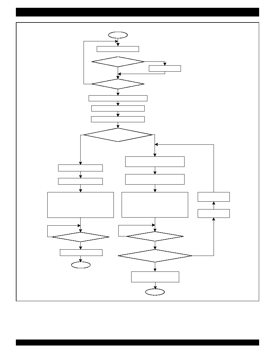
33
RSLIC (IDT82V1671) & CODEC (IDT82V1074) CHIPSET INDUSTRIAL TEMPERATURE RANGE
Figure - 16 Recommended Programming Flow Chart for FSK Generation
Read GREG23
FSK_EN = 1 ?
FSK_TS = 0 ?
FSK_EN = 1
Set Seizure Length (GREG21)
Set Mark Length (GREG22)
Set Flag Length (GREG19)
Total Caller ID data =< 64 bytes ?
Set Data Length (GREG20)
Write CID data into FSK-RAM
In GREG23:
- Select a channel by setting bits FSK_CS[1:0];
- Select a standard by setting bit FSK_BS;
- FSK_MAS = 0;
- FSK_TS = 1
Set the length of the Caller ID data to be
sent at this time (GREG20)
Write the Caller ID data to be sent at this
time to the FSK-RAM
Finish sending all Caller ID data ?
FSK_MAS = 0
FSK_EN = 0
End
Seizure Length = 0
Mark Length = 0
End
Start
N
Y
FSK_TS = 0 ?
FSK_EN = 0
Y
N
Y
N
Y
N
Y
N
FSK_TS = 0 ?
Y
N
In GREG23:
- Select a channel by setting bits FSK_CS[1:0];
- Select a standard by setting bit FSK_BS;
- FSK_MAS = 1;
- FSK_TS = 1

34
RSLIC (IDT82V1671) & CODEC (IDT82V1074) CHIPSET INDUSTRIAL TEMPERATURE RANGE
3.7.3
UNIVERSAL TONE DETECTION (UTD)
3.7.3.1
Introduction
The RSLIC-CODEC chipset provides optimized solution not only for
voice transmission, but for modem data transmission. The performance
of the latter is becoming a key performance for the increasing internet
access and other data applications. The chipset's universal tone (fax/
modem tone) detection allows the use of modem-optimized filter for V.34
and V.90 connections.
The CODEC provides an integrated Universal Tone Detection (UTD)
unit per channel to detect fax and modem tones from the transmit or
receive path. The UTD unit can detect tone signals whose frequencies
are between 1500 Hz and 2600 Hz.
If a fax or modem tone is detected, which means that a modem
connection is about to be established
, the lowpass filter (see
Figure - 9
on page 20
) characteristic is changed to a modem-optimized one. If the
modem data transmission is completed, the lowpass filter characteristic
will be switched back to the voice-optimized one for voice data
transmission. With this mechanism implemented in the chipset, the
optimum modem transmission rate can always be achieved.
The characteristic of the lowpass filter can be changed by software. If
the V90 bit in register LREG5 is set to 1, this filter will be configured for
V90 connections (modem-optimized), otherwise it will be configured for
V34 connections (voice-optimized).
3.7.3.2
UTD Principle
As shown in
Figure - 17
(UTD Functional Block Diagram), the input
signal from transmit or receive path is first filtered by a programmable
bandpass filter and a programmable bandstop filter separately. The in-
band (upper path) and out-of-band (lower path) signals are then
separated from each other and the corresponding absolute values are
calculated. The two calculated results are sent to two integrators,
respectively. Finally, the evaluation logic block determines whether a
tone is detected by comparing the in-band level with the out-of-band
level.
If a tone has been detected in the receive or transmit path, the
UTD_OK bit in LREG21 will be set to 1 and an interrupt will be
generated.
The UTD_OK bit will be set to 1 if all the following conditions hold for
a time span of at least a Recognition Time (RTime, programmable by
LREG14) without occurring breaks longer than a Recognition Break
Time (RBRKTime, programmable by LREG15):
∑ The in-band signal level is higher than out-band signal level.
∑ The in-band signal level is higher than the floor threshold
(programmable by word UTDthld_Floor in the Coe-RAM).
∑ The in-band signal level is lower than the ceiling threshold
(programmable by word UTDthld_Ceiling in the Coe-RAM).
Figure - 18
shows an example of UTD recognition timing.
The UTD_OK bit will be reset to 0 if one of the preceding conditions
is violated for at least a time span of an End Detection Time (ETime,
programmable by LREG16) during which the violation does not cease
for at least an End Detection Break Time (EBRKTime, programmable by
LREG17). Refer to
Figure - 19
for an example of UTD tone end
detection timing.
Figure - 17 UTD Functional Diagram
|X|
|X|
Integrator
Evaluation Logic
Signal In
Programmable Bandpass Filter
Programmable Bandstop Filter
Integrator
Detection Result
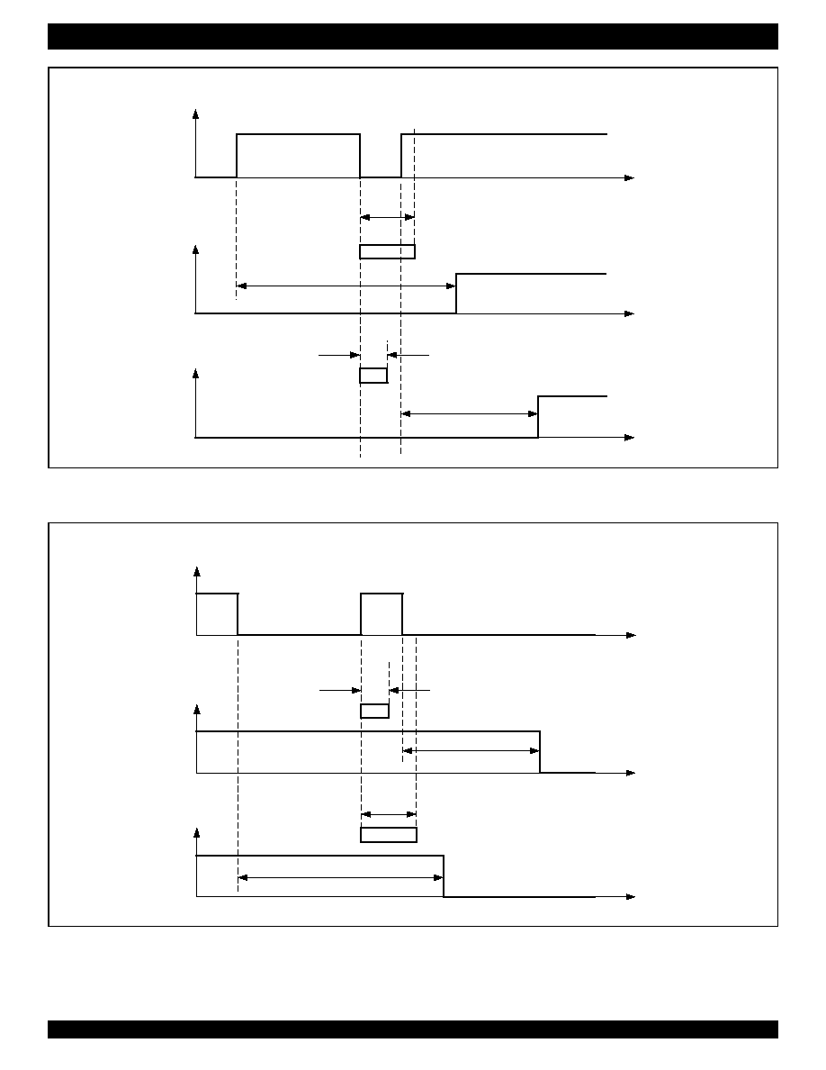
35
RSLIC (IDT82V1671) & CODEC (IDT82V1074) CHIPSET INDUSTRIAL TEMPERATURE RANGE
Figure - 18 Example of UTD Recognition Timing
Figure - 19 Example of UTD Tone End Detection Timing
RBRKTime
RTime
RBRKTime
Tone
UTD-OK
RTime
UTD-OK
t
t
t
EBRKTime
ETime
EBRKTime
ETime
UTD-OK
Tone
UTD-OK
t
t
t

36
RSLIC (IDT82V1671) & CODEC (IDT82V1074) CHIPSET INDUSTRIAL TEMPERATURE RANGE
3.7.3.3
UTD Programming
Table - 10
shows the registers and Coe-RAM locations used for the
UTD unit.
The UTD unit can be enabled or disabled individually for each
channel by the UTD_EN in register LREG8. The UTD_SRC bit in
LREG8 determines whether the signal from transmit or receive path is
detected. The RTime, RBRKTime, ETime and EBRKTime of the UTD
are programmed by LREG14, LREG15, LREG16 and LREG17,
respectively.
If the UTD bit in LREG5 is set to 0, the coefficients of the bandpass
and the bandstop filters and the thresholds of the signal are
programmable via the Coe-RAM. The center frequencies of the two
filters should be the same. The center frequency can be programmed
from 1500 Hz to 2600 Hz. The bandwidths of the two filters are also
programmable. The ceiling and floor thresholds of the signal can be
programmed from
-30 dBm to 0 dBm in minimum steps of 0.2 dBm.
IDT provides a software (Cal74) to calculate the filter and threshold
coefficients. When users input the desired center frequency, bandwidth
for the two filters and ceiling threshold, floor threshold for the signal, the
software will automatically calculate all the coefficients for the UTD unit.
After loading these coefficients to the Coe-RAM, the performance of the
UTD unit will meet the users' requirements. Refer to
Table - 23 on page
62
for the Coe-RAM mapping.
If the UTD bit is set to 1, the filter coefficients and the thresholds in
the ROM are used. These values are used by default. See
Table - 10 for
details.
Table - 10 Registers and Coe-RAM Locations Used for UTD
Parameter
Register Bits/Coe-RAM Words
Notes
UTD Unit Enable
Bit UTD_EN in LREG8
UTD_EN = 0: the UTD unit is disabled;
UTD_EN = 1: the UTD unit is enabled.
UTD Source Selection
Bit UTD_SRC in LREG8
UTD_SRC = 0: signal from receive path is detected;
UTD_SRC = 1: signal from transmit path is detected.
UTD Result Indication
Bit UTD_OK in LREG21
UTD_OK = 0: no fax/modem tone has been detected;
UTD_OK = 1: fax/modem tone has been detected.
UTD RTime
Bits UTD_RT[7:0] (LREG14)
Recognition time, programmable from 0 to 4000 ms. The default value is
304 ms.
UTD RBRKTime
Bits UTD_RBK[7:0] (LREG15)
Recognition break time, programmable from 0 to 1000 ms. The default
value is 100 ms.
UTD ETime
Bits UTD_ET[7:0] (LREG16)
End detection time, programmable from 0 to 1000 ms. The default value is
256 ms.
UTD EBRKTime
Bits UTD_EBRK[7:0] (LREG17)
End detection break time, programmable from 0 to 255 ms. The default
value is 100 ms.
UTD Filter Coefficients and Signal
Thresholds Selection
Bit UTD in LREG5
UTD = 0: The signal thresholds and filter coefficients written in the Coe-
RAM are selected.
UTD = 1: The signal thresholds and filter coefficients in the ROM are
selected (default);
UTD Bandpass Filter Coefficient
UTD Bandpass Filter Coefficient in the Coe-RAM
The center frequency is programmable from 1500 Hz to 2600 Hz. The
default center frequency and bandwidth (in the ROM) are 2100 Hz and 60
Hz respectively.
UTD Bandstop Filter Coefficient
UTD Bandstop Filter Coefficient in the Coe-RAM
The center frequency is programmable from 1500 Hz to 2600 Hz. The
default center frequency and bandwidth (in the ROM) are 2100 Hz and
230 Hz respectively.
UTD Signal Ceiling Threshold
UTDthld_Ceiling in the Coe-RAM
Programmable from
-30 dBm to 0 dBm in minimum steps of 0.2 dBm. The
default value (in the ROM) is
-6 dBm.
UTD Signal Floor Threshold
UTDthld_Floor in the Coe-RAM
Programmable from
-30 dBm to 0 dBm in minimum steps of 0.2 dBm. The
default value (in the ROM) is
-18 dBm.

37
RSLIC (IDT82V1671) & CODEC (IDT82V1074) CHIPSET INDUSTRIAL TEMPERATURE RANGE
3.8
THREE-PARTY CONFERENCE
3.8.1
INTRODUCTION
The RSLIC-CODEC chipset provides a three-party conference
facility on the PCM interface in MPI mode only. With this facility, either an
external three-party conference or an internal three-party conference
can be held without additional hardware.
Figure - 20
shows the conference block diagram. When an external
conference mode is selected (GREG7: CONFX_EN=1), the chipset acts
as a server for three external calling partners (B, C and D) to hold a
conference with each other. When an internal conference mode is
selected (GREG7: CONF_EN=1), a conference can be held between an
internal calling partner (S) and two external calling partners (B and C).
The internal calling partner is a subscriber connected to one of the four
channels of the local CODEC. The external calling partners do not need
any conference facility, for the chipset performs all the functions required
by a conference for them.
The three-party conference facility consists of adders, gain stages,
PCM configuration registers and a conference control register. The voice
data in the receive time slots of any two partners is added by the adder
and sent to the transmit time slot of the third partner. The registers
GREG9, GREG11 and GREG13 are used to select transmit PCM
highway and time slot for the three partners. The registers GREG10,
GREG12 and GREG14 are used to select receive PCM highway and
time slot for the three partners. To avoid overflow of the sum signals, a
programmable gain stage (G) is used. The gain is programmed by
GREG8. The CONF_EN and CONFX_EN bits in GREG7 are used to
select the internal and external conferences respectively. If internal
conference is selected, the CONF_CS[1:0] bits in GREG7 are used to
select one of the four channels of the local CODEC to attend the
conference.
Both A/µ-law compressed (8-bit) and linear (16-bit 2's complement)
voice data can be transferred in a three-party conference. If compressed
data format is selected, at least 7 time slots are needed in the transmit/
receive PCM highway to perform a three-party conference and use the
four local channels at the same time (three time slots for partners B, C
and D, four time slots for local Channel 1 to 4). So the lowest BCLK
frequency should be 512 kHz, corresponding to 8 time slots available.
3.8.2
PCM INTERFACE CONFIGURATION
The PCM interface can be configured to work in different mode as
shown in
Table - 11
. The P_DOWN bit in LREG6 is used to power down
the specify channel of the CODEC. When all four channels of the
chipset are powered down, no data is transferred via the PCM highways.
The P_DOWN bit together with the CONF_EN and CONFX_EN bits
control the conference behavior and the PCM line drivers.
Figure - 20 Conference Block Diagram
R3
R2
R4
X3
X4
X2
D
C
B
D
C
B
+
G
0
1
CONF_EN=0
G
+
+
G
0
1
CONF_EN=0
-
-
-
+
+
+
A
A
Subscriber S
PCM Highway1
PCM Highway2
G: Gain Stage (Gain Factor) programmed by GREG8
X1 - X4: 4 time slots in transmit PCM highway
R1 - R4: 4 time slots in receive PCM highway
A, B, C, D:
External calling partners
S:
Internal calling partner, which is connected to one of the four channels of the local CODEC.
R1
X1

38
RSLIC (IDT82V1671) & CODEC (IDT82V1074) CHIPSET INDUSTRIAL TEMPERATURE RANGE
∑ PCM Off
When the chipset is just reset, or in the power down state, no data is
transferred via the PCM highways. Also when selecting new time slots,
it's recommended to switch off the PCM line drivers by setting the
corresponding P_DOWN bit to 1, CONF_EN bit and CONFX_EN bit to
0.
∑ PCM Active
This is the normal operating mode without conference. Only time
slots R1 and X1 are used. Voice data is transferred from an external
subscriber A to an internal subscriber S.
∑ External Conference
In this mode the chipset acts as a conferencing server for
subscribers B, C and D. These three partners may be controlled by any
device connected to the PCM highways. To reduce the power
consumption, the channels of the local CODEC can be powered down if
they are not being used.
∑ External Conference + PCM Active
As in the external conference mode, any external three-party
conference is supported in this mode. At the same time, if the channels
of the local CODEC are powered on (active), the subscribers connected
to the corresponding channels can make normal phones calls.
∑ Internal Conference
If the subscriber S is one of the conference partners, the internal
conference mode should be selected. Then, A three-party conference
can be held between the internal partner S and the external partners B
and C. In this mode, the CODEC channel which the partner S is
connected must be powered on.
3.8.3
CONTROL THE ACTIVE PCM CHANNELS
Table - 12
shows the register configuration for the transmit PCM
channels. For details refer to
"4.1.2 PCM Interface" on page 51
.
Table - 11 Conference Mode
Configuration Bits
Receive Time Slots
Transmit Time Slots
Mode
P_DOWN
(LREG6)
CONF_EN
(GREG7)
CONFX_EN
(GREG7)
R1
R2
R3
R4
X1
X2
X3
X4
Subscriber S
PCM Off
1
0
0
-
-
-
-
Off
Off
Off
Off
Off
PCM Active
0
0
0
A
-
-
-
S
Off
Off
Off
A
External Conference
1
0
1
-
B
C
D
Off
G(C+D)
G(B+D)
G(B+C)
Off
External Conference
+ PCM Active
0
0
1
A
B
C
D
S
G(C+D)
G(B+D)
G(B+C)
A
Internal Conference
0
1
0
-
B
C
-
Off
G(C+S)
G(B+S)
Off
G(B+C)
Table - 12 Active PCM Channel Configuration Bits
Control Bits
Transmit PCM Time Slot
P_DOWN
(LREG6)
CONF_EN
(GREG7)
CONFX_EN
(GREG7)
L_CODE
(GREG3)
X1
X2
X3
X4
1
0
0
-
-
-
-
-
0
0
0
0
PCM
-
-
-
0
0
0
1
HB LB
-
-
-
0
1
0
0
-
PCM
PCM
-
0
1
0
1
-
HB LB
HB LB
-
0
1
0
0
PCM
PCM
PCM
-
0
1
0
1
HB LB
HB LB
HB LB
-
1
0
1
0
-
PCM
PCM
PCM
1
0
1
1
-
HB LB
HB LB
HB LB
0
0
1
0
PCM
PCM
PCM
PCM
0
0
1
1
HB LB
HB LB
HB LB
HB LB
1
1
1
0
-
PCM
PCM
PCM
1
1
1
1
-
HB LB
HB LB
HB LB
0
1
1
0
PCM
PCM
PCM
PCM
0
1
1
1
HB LB
HB LB
HB LB
HB LB

39
RSLIC (IDT82V1671) & CODEC (IDT82V1074) CHIPSET INDUSTRIAL TEMPERATURE RANGE
NOTES:
In
Table - 11
and
Table - 12
:
1. The `P_DOWN' bit (in register LREG6) is used to power down the corresponding channel of the CODEC: P_DOWN = 1, power down; P_DOWN = 0, power on.
2. The `L_CODE' bit (in register GREG3) is used to select the PCM data format: L_CODE = 1, linear code; L_CODE = 0, A/µ-law compressed code.
3. 'PCM' means PCM compressed data (A-law/µ-law).
4. HB and LB represent the high byte and low byte of the linear data respectively.
5. Modes in rows with gray background are for testing purpose only.

40
RSLIC (IDT82V1671) & CODEC (IDT82V1074) CHIPSET INDUSTRIAL TEMPERATURE RANGE
3.9
ITDF
3.9.1
INTRODUCTION
Subscriber lines are often affected by many types of failures, e.g.,
short circuits, broken lines, leakage currents, noise etc. Service
providers must be able to perform line tests and respond quickly if there
are any failures.
Traditional line cards solutions usually need external relays and test
equipment to accomplish line tests. The RSLIC-CODEC chipset
provides integrated test and diagnosis functions (ITDF) that can monitor
and diagnose line faults and line card device failures without test relays
or test equipment. With the ITDF implemented, the chipset increases the
test possibilities, reduces the testing time and cost and provides more
flexibility for system manufacturers and service providers over traditional
solutions.
3.9.2
DIAGNOSIS AND TEST FUNCTIONS
A set of signal generators and features are implemented in the
chipset to accomplish various diagnosis functions. The CODEC
generates an appropriate test signal, applies it to the loop, measures the
resulting voltage or current signal level and reports the result to a master
microprocessor. All the tests can be initiated by the microprocessor and
results can be read back very easily. By monitoring the subscriber loop,
the ITDF might prevent any problems caused by the subscriber line or
line equipment from affecting the service.
The chipset can accomplish the following test and measurement
functions:
∑ Loop resistance
∑ Leakage current Tip/Ring
∑ Leakage current Tip/GND
∑ Leakage current Ring/GND
∑ Ringer capacitance
∑ Line capacitance
∑ Line capacitance Tip/GND
∑ Line capacitance Ring/GND
∑ External voltage measurement Tip/GND
∑ External voltage measurement Ring/GND
∑ External voltage measurement Tip/Ring
∑ Measurement of ringing voltage
∑ Measurement of line feed current
∑ Measurement of supply voltage VDD of the CODEC
∑ Measurement of transversal and longitudinal currents
3.9.3
INTEGRATED SIGNAL GENERATORS
The signal generators available on the chipset are as follows:
∑ Constant DC voltage generation (programmable ringing DC offset
voltages);
∑ Two independent tone generators (TG1 and TG2) per channel
(used to generate DTMF signal and various test tones. Please
refer to
"3.7.1 Tone Generator" on page 30
for details);
∑ Ramp generator (used for capacitance measurement, refer to
page 47
for details);
∑ Ring generator (used to generate an internal balanced ringing
signal. Refer to
"3.4.1.1 Internal Ringing Generation" on page 23
for details).
3.9.4
LEVEL METER
An on-chip level meter together with the signal generators mentioned
accomplishes all test and diagnosis functions.
Figure - 21
on the
following page shows the entire level meter block diagram.
3.9.4.1
Level Meter Source Selection
The level meter is shared by all four channels. The LM_CS[1:0] bits
in register GREG16 select one of the channels for level metering. For
each channel, there are one AC signal source and ten DC signal
sources to be selected. The LM_SRC and DC_SRC bits in register
LREG8 and the LM_SEL[3:0] bits in register LREG9 make the selection.
See
Table - 13
for details.
Attention: The VTDC is selected as the level meter source by
default. When the CODEC works in active mode, it automatically adjusts
the DC feeding according to the DC voltage on the VTDC pin. So,
selecting inputs VL, IO3, IO4, IO3-IO4, DCN-DCP or VDD/2 as the level
meter source may disturb the DC feeding regulation and cause
problems in the DC loop. To avoid this, users can freeze the output of
the DC loop before selecting these inputs as the sources by setting the
ACTIVE bit in LREG6 to 0.
∑ AC Level Meter
If the LM_SRC bit in register LREG8 is set to 1, the AC signal in the
transmit path (VTAC) is selected for level metering.
The AC level meter can measure the voice signal at 8 kHz while the
active voice signal is being processed (see
Figure - 21
). After being pre-
filtered, A/D converted and decimated, the signal can be filtered by a
programmable filter. The LM_FILT bit LREG8 determines whether the
filter is enabled. If the filter is enabled, the LM_NOTCH bit in LREG8
determines which filter characteristic (notch or bandpass) is selected.
LM_FILT = 0:
the filter is disabled (normal operation);
LM_FILT = 1:
the filter is enabled;
LM_NOTCH = 0: notch filter characteristic is selected;
LM_NOTCH = 1: bandpass filter characteristic is selected.
The filter coefficients can be from the Coe-RAM or from the ROM, as
selected by the LM_N and LM_B bits in LREG5.
LM_N = 0:
the coefficient in the Coe-RAM is used for the
notch filter;
Table - 13 Level Meter Source Selection
LM_SRC
DC_SRC
LM_SEL[3:0]
Level Meter Source
1
x
xxxx
AC signal in transmit path (VTAC)
0
0
xxxx
Digital DC signal
0
1
0000
DC voltage on VTDC (default)
0
1
0100
DC output voltage on DCN-DCP
0
1
1001
DC voltage on VL
0
1
1010
Voltage on IO3
0
1
1011
Voltage 0n IO4
0
1
1100
Voltage on RTIN
0
1
1101
VDD/2
0
1
1110
Offset voltage (VCM is selected)
0
1
1111
Voltage on IO4-IO3
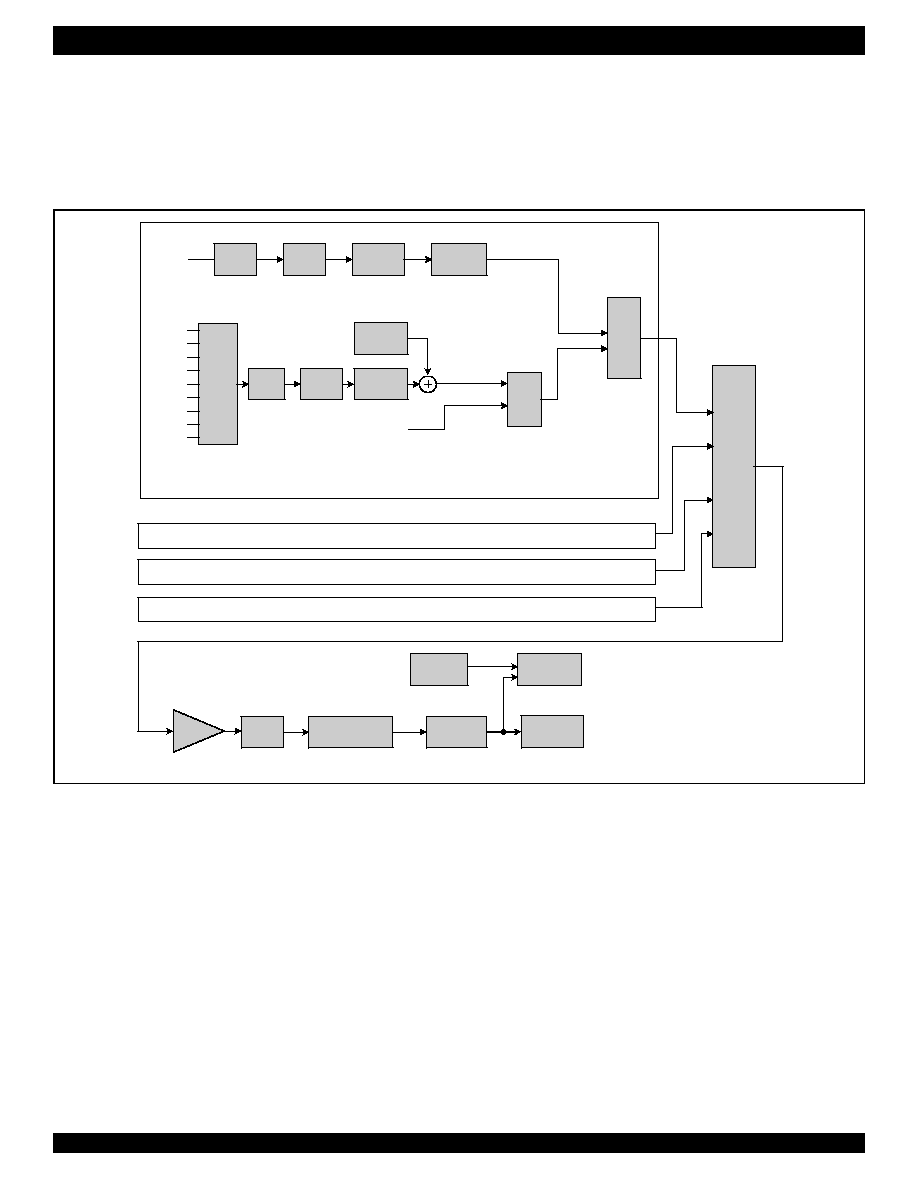
41
RSLIC (IDT82V1671) & CODEC (IDT82V1074) CHIPSET INDUSTRIAL TEMPERATURE RANGE
LM_N = 1:
the coefficient in the ROM is used for the notch
filter;
LM_B = 0:
the coefficient in the Coe-RAM is used for the
bandpass filter;
LM_B = 1:
the coefficient in the ROM is used for the
bandpass filter;
The center frequency of the notch/bandpass filter is programmable
from 300 Hz to 3400 Hz. The default center frequency is 1014 Hz. The
quality factor (Q) is fixed to 5. The filter coefficients are automatically
calculated by a software (Cal74) provided by IDT. When users input the
center frequency, this software will calculate the coefficient for the notch
or bandpass filter. By loading the coefficients to the Coe-RAM of the
CODEC, the filter characteristic can meet the requirements. Refer to
Table - 23 on page 62
for the Coe-RAM mapping.
∑ DC Level Meter
If the LM_SRC bit in register LREG8 is set to 0, the DC level meter is
selected to perform the measurement. The DC signal source can be
from transmit or receive path depending on the DC_SRC bit in register
LREG8:
DC_SRC = 0: DC signal (digital) from receive path is selected;
DC_SRC = 1: DC signal from transmit path is selected.
There are a total of nine DC signal sources in the transmit path. They
are specified by the LM_SEL[3:0] bits in register LREG9. Refer to
Table
- 13
for details.
As
Figure - 21
shows, the selected signal from DC transmit path is
filtered, A/D converted and decimated. The effective sampling rate after
the decimation stage is 8 kHz. The Offset Register here is used to
compensate for the current and voltage offset errors. See
"3.9.6.1 Offset
Current Measurement" on page 45
and
"3.9.6.7 Voltage Offset
Measurement" on page 49
for details.
3.9.4.2
Level Meter Gain Filter and Rectifier
The selected signal from the AC or DC path is further processed by a
programmable digital gain filter. The additional gain factor is either 1 or
16 depending on the LM_GF bit in register LREG10:
LM_GF = 0:
No additional gain factor;
LM_GF = 1:
Additional gain factor of 16.
The LM_GF bit should be set to 0 unless the tested signal is small
enough.
A rectifier follows to change the minus signal to plus signal. It can be
enabled or disabled by the LM_RECT bit in register LREG10:
LM_RECT = 1: rectifier enabled;
LM_RECT = 0: rectifier disabled.
Figure - 21 Level Meter Block Diagram
Filter
A/D
2 MHz
Decimation
Bandpass/
Notch Filter
Rectifier
Shift
Factor
Integrator
Result
Register
VTAC
MUX
A/D
1 MHz
Decimation
VTDC
VL
IO3
IO4
VDD/2
Filter
Offset
Register
IO4-IO3
MUX
VRDC
RTIN
MUX
Comparator
Threshold
Register
16/1
CHANNEL1
CHANNEL2
CHANNEL3
CHANNEL4
MUX
Bit DC_SRC in LREG8
Bits LM_FILT and LM_NOTCH in LREG8
Bits LM_B and LM_N in LREG5
LM bandpass filter coefficient
LM notch filter coefficient
VCM
Bits LM_SEL[3:0] in LREG9
Bit LM_SRC in LREG8
Bits LM_TH[2:0]
in LREG10
Bits K[3:0] in LREG9
Bits LM_EN and LM_ONCE in GREG16
Bits LM_CN[10:0] in GREG15 and GREG16
Bit LM_RECT in
LREG10
Bit LM_GF in
LREG10
Bit LM_OK in LREG21
Bits LM_CS[1:0]
in LREG10
DC Path
AC Path
Bit OTHRE in LREG10
From Transmit
From Receive
Bits LMRL[7:0] in GREG17
Bits LMRH[7:0] in GREG18
Bit DC_OFT in LREG4
Word DC Offset in the Coe-RAM
Digital DC signal
DCN-DCP

42
RSLIC (IDT82V1671) & CODEC (IDT82V1074) CHIPSET INDUSTRIAL TEMPERATURE RANGE
3.9.4.3
Level Meter Integrator
An integrator is used to accumulate and sum up the signal values
over a preset period. The accumulation period (count number) is
programmable from 0 to 255.875 ms in steps of 0.125 ms, by the bits
LM_CN[10:0] in registers GREG15 and GREG16. The integrator can be
configured to run once or continuously by the LM_ONCE bit in GREG16:
LM_ONCE = 0: integrator runs continuously;
LM_ONCE = 1: integrator runs once.
In continuous mode, the integrator starts to accumulate the samples
after the LM_EN bit in register GREG16 is set to 1. When the count
number is reached, which means that once integration is finished, the
LM_OK bit in LREG21 will be set to 1 and an interrupt will be generated.
The next integration starts right after the previous integration is finished,
and the LM_OK bit will be automatically reset after 125 µs. The
integrator runs continuously in this way and will not stop unless the
LM_EN bit is set to 0.
Figure - 22
shows the continuous measurement
sequence.
In single mode, the integrator works only once after each initiation
(LM_EN = 1). Once the integration is finished, the LM_OK bit will be set
to 1 and will not be reset until the LM_EN bit is set to 0. To start a new
integration, the LM_EN bit must be changed from 0 to 1. The single
measurement sequence is illustrated in
Figure - 23
.
Figure - 22 Continuous Measurement Sequence (AC & DC Level Meter)
GREG16: LM_EN
LREG21: LM_OK
125
µs
125
µs
125
µs
Int. Period
Int. Period
Int. Period
Int. Period
GREG16: LM_ONCE = 0
Read Result
GREG17 & GREG18
Read Result
GREG17 & GREG18
Read Result
GREG17 & GREG18
Figure - 23 Single Measurement Sequence (AC & DC Level Meter)
Int. Period
Int. Period
GREG16: LM_EN
GREG16: LM_ONCE = 1
Start New Measurement
LREG21: LM_OK
Read Result
(GREG17 & GREG18)

43
RSLIC (IDT82V1671) & CODEC (IDT82V1074) CHIPSET INDUSTRIAL TEMPERATURE RANGE
In both continuous and single modes, the level meter result LM
Value
is sent to registers GREG17 & GREG18 after every integration period.
To calculate the measured signal level, a factor LM
Result
is defined as:
The number of samples N
Samples
for the integrator is calculated by:
N
Samples
= LM_CN
Where, LM_CN is the level meter count number (set by bits
LM_CN[10:0] in registers GREG15 & GREG16).
Then the signal level can be calculated by the following formula:
Where, K
INT
is the selected shift factor. Refer to
"3.9.4.5 Level Meter
Shift Factor"
for details.
3.9.4.4
Level Meter Result Register
The level meter result is a 16-bit 2's complement. The low byte and
high byte of it are stored in registers GREG17 and GREG18
respectively.
Table - 14
shows the range of the result value.
3.9.4.5
Level Meter Shift Factor
As the level meter result is a 16-bit 2's complement while the
integration width is 27 bits, a shift factor is necessary to avoid generating
an overflow in result registers and make the results with maximum
accuracy. The shift factor K
INT
is programmed by register LREG9. See
Table - 15
for details.
3.9.4.6
Level Meter Threshold Setting
Once the level meter result is latched in the result registers, it will be
compared with a programmable threshold. If the absolute value of the
result exceeds the threshold, the OTHRE bit in register LREG10 will be
set to 1.
This threshold is a percentage value of the full scale (see
Table - 14
).
It is programmed by the LM_TH[2:0] bits in LREG10. Refer to
Table - 16
for details.
Table - 14 Level Meter Result Value Range
Negative Value Range
Positive Value Range
- Full scale
+ Full scale
0x8000
0xFFFF
0
0x7FFF
- 32768
- 1
0
+ 32768
LM
Result
LM
Value
32768
-----------------------
=
Udbm0
20
LM
Result
2 K
INT
N
Samples
◊
◊
-----------------------------------------------
◊
log
◊
3.14
+
=
Table - 15 Shift Factor Selection
K[3:0] bits in LREG9
Shift Factor
0000
K
INT
= 1
0001
K
INT
= 1/2
0010
K
INT
= 1/4
0011
K
INT
= 1/8
0100
K
INT
= 1/16
0101
K
INT
= 1/32
0110
K
INT
= 1/64
0111
K
INT
= 1/128
1000
K
INT
= 1/256
1001
K
INT
= 1/512
1010
K
INT
= 1/1024
1011 to 1111
K
INT
= 1/2048
Table - 16 Level Meter Threshold Setting
LM_TH[2:0] in LREG10
Threshold
LM_TH[2]
LM_TH[1]
LM_TH[0]
0
0
0
0%
0
0
1
12.5%
0
1
0
25.0%
0
1
1
37.5%
1
0
0
50.0%
1
0
1
62.5%
1
1
0
75.0%
1
1
1
87.5%

44
RSLIC (IDT82V1671) & CODEC (IDT82V1074) CHIPSET INDUSTRIAL TEMPERATURE RANGE
Table - 17
sums up the registers and Coe-RAM locations used for the
level meter.
Table - 17 Registers and Coe-RAM Locations Used for the Level Meter
Parameter
Register Bits/Coe-RAM Words
Notes
Level meter channel selection
LM_CS[1:0] bits in GREG16
The LM_CS[1:0] bits determine the signal from which channel to be level
metered.
Level meter source selection
LM_SRC and DC_SRC bits in LREG8
LM_SEL[3:0] bits in LREG9
Refer to
Table - 13
for details.
Level meter shift factor selection K[3:0] bits in LREG9
Refer to
Table - 15
for details.
Level meter count number
(integration time) selection
LM_CN[10:0] bits in GREG15 & GREG16
The LM_CN[10:0] bits is programmable from 0 to 7FFH, corresponding to the
integration time of 0.125 ms to 255.875 ms.
Level meter result
LMRL[7:0] bits in GREG17 (low byte)
LMRH[7:0] bits in GREG18 (high byte)
See
Table - 14
for details.
Level meter threshold
Threshold selection: LM_TH[2:0] bits in LREG10
Over threshold indication: OTHRE bit in LREG10
Refer to
Table - 16
for details on threshold selection. Once the selected threshold
is exceeded, the OTHRE bit will be set to 1.
Level meter bandpass/notch
filter configuration
LM_FILT and LM_NOTCH bits in LREG8
LM_FILT = 0: bandpass/notch filter is disabled;
LM_FILT = 1: bandpass/notch filter is enabled;
LM_NOTCH = 0: notch filter characteristic is selected;
LM_NOTCH = 1: bandpass filter characteristic is selected.
Level meter bandpass/notch
filter coefficient selection
LM_B and LM_N bits in LREG5
LM_B = 0: The coefficient in the Coe-RAM is selected for the bandpass filter;
LM_B = 1: The coefficient in the ROM is selected for the bandpass filter (default);
LM_N = 0: The coefficient in the Coe-RAM is selected for the notch filter;
LM_N = 1: The coefficient in the ROM is selected for the notch filter (default).
LM Bandpass Filter Coefficient LM Bandpass Filter Coefficient in the Coe-RAM When LM_B = 1, this coefficient will be selected for the bandpass filter.
LM Notch Filter Coefficient
LM Notch Filter Coefficient in the Coe-RAM
When LM_N = 1, this coefficient will be selected for the notch filter.
Level meter enable
LM_EN bit in GREG16
A logic high in this bit starts a level meter measurement while a logic low stops
the measurement.
Indication of Level meter
measurement completed
LM_OK bit in LREG21
Once the measurement is finished, the LM_OK bit will be set to 1.
Level meter gain filter
configuration
LM_GF bit in LREG10
This bit selects a gain factor of 1 or 16 for the level meter gain filter.
Level meter rectifier enable
LM_RECT bit in LREG10
This bit is used to enable or disable the level meter rectifier as required.
Level meter integrator work
mode
LM_ONCE bit in GREG16
This bit determines whether the integrator works once or continuously.
Offset Register in the level
meter
DC_OFT bit in LREG4
word DC Offset in the Coe-RAM
DC_OFT = 0: The compensation value in the Coe-RAM is selected for the Offset
Register;
DC_OFT = 1: The default compensation value of 0 is selected for the Offset
Register.

45
RSLIC (IDT82V1671) & CODEC (IDT82V1074) CHIPSET INDUSTRIAL TEMPERATURE RANGE
3.9.5
MEASUREMENT VIA AC LEVEL METER
3.9.5.1
Current Measurement via VTAC
In order to measure current via the VTAC pin, all feedback loops
(impedance matching filters and transhybrid balance filter) should be
disabled. To simplify the formulas, the programmable receive and
transmit gain (GTX, FRX, GRR and FRR) are disabled by corresponding
registers (refer to
"3.3.2 Programmable Filters" on page 21
for details).
Based on this a factor K
ADAC
(gain of analog to digital in AC loop) can be
defined:
The transversal current I
RMS
measured at the RSLIC:
LM
Result:
LM
Result
= LM
Value
/ 32768
N
Samples:
N
Samples
= LM_CN
K
INT:
Value of the shift factor
K
ITAC:
Value of the AC current to voltage converter for
transversal voltage (R
Sense
is the sense resistance)
3.9.5.2
AC Level Meter Operational State Flow
The operational state flow for the AC level meter is as the following:
1. The level meter is in the disable state (LM_EN = 0), the result
registers (GREG17 & GREG18) are cleared.
2. Set the level meter count number (LM_CN[10:0]) in registers
GREG15 and GREG16.
3. Enable the level meter (LM_EN =1) and it starts to accumulate
the samples. When the preset count number is reached, the
LM_OK bit is set and the accumulation result will be latched into
the result registers simultaneously. If the result exceeds the
preset threshold, the OTHRE bit in LREG10 will be set.
4. If the LM_ONCE bit is 0 (continuous mode), the level meter
continues to measure the next samples right after one
measurement is finished, the LM_OK bit is reset after 125 µs.
5. If the LM_ONCE bit is 1 (single mode), the level meter runs one
time after the it is initiated and the LM_OK bit will not be reset until
the LM_EN bit is set to 0.
3.9.6
MEASUREMENT VIA DC LEVEL METER
3.9.6.1
Offset Current Measurement
The current offset error is caused by the current sensor inside the
RSLIC. The current offset can be measured by the DC level meter. The
following settings are necessary to accomplish this measurement:
∑ The RSLIC is set to Normal Active mode (for MPI interface,
LREG6: SCAN_EN = 1, SM[2:0] = 000; for GCI interface,
downstream C/I channel: SCAN_EN = 1, SM[2:0] = 000) and the
loop is on-hook. In this condition, there should be no current
present, but the current sensor incorrectly indicates a current
flowing (current offset error).
∑ Select VTDC and VL to the DC level meter separately (by setting
bits LM_SEL[3:0] in LREG9 to `0000' and `1001' respectively).
∑ The value in the Offset Register must be set to 0 (by clearing the
word/DC Offset in the Coefficient RAM).
∑ Then the transversal and longitudinal offset currents (I
Tdc,Off-Err
and I
Ldc,Off-Err
) can be calculated.
K
ITDC:
Value of the DC current to voltage converter for
transversal current (R
Sense
is the sense resistance)
K
IL:
Value of the current to voltage for longitudinal current
K
INT:
Value of the shift factor
K
ADDC:
Gain of analog to digital conversion in the DC loop
3.9.6.2
Leakage Current Measurement
The leakage current Tip/Ring, leakage current Tip/GND and leakage
current Ring/GND can be measured by the DC level meter when the
RSLIC is in on-hook mode. The following settings are necessary to
accomplish the leakage current measurement:
∑ The RSLIC must be set to Normal Active mode when measuring
the leakage current Tip/Ring.
∑ The RSLIC must be set to Tip Open mode when measuring the
leakage current Ring/GND.
∑ The RSLIC must be set to Ring Open mode when measuring the
leakage current Tip/GND.
∑ Select VTDC to the DC level meter (LREG9: LM_SEL[3:0]= 0000);
∑ I
Leakage
can be calculated as shown below:
K
ADAC
1
=
I
RMS
LM
Result
◊
K
ADAC
K
INT
◊
N
Samples
◊
K
ITAC
◊
2
◊
2
◊
------------------------------------------------------------------------------------------------
=
K
ITAC
8 R
Sense
◊
=
V
Tdc Off
,
Err
≠
LM
Result
K
ADDC
K
INT
◊
N
Samples
◊
------------------------------------------------------------------
=
V
Ldc Off
,
Err
≠
LM
Result
K
ADDC
K
INT
◊
N
Samples
◊
------------------------------------------------------------------
=
I
Tdc Off
,
Err
≠
V
Tdc Off
,
Err
≠
K
ITDC
---------------------------------
=
I
Ldc Off
,
Err
≠
V
Ldc Off
,
Err
≠
K
IL
--------------------------
=
K
ITDC
2
5
--- R
Sense
◊
=
K
IL
R
Sense
=
K
ADDC
1
2
---
=
I
Leakage TipIEND
≠
LM
Result
2
◊
K
ADDC
K
INT
◊
N
Samples
◊
K
ITDC
◊
-----------------------------------------------------------------------------
I
Tdc Off
,
Err
≠
I
Ldc Off
,
Err
≠
≠
2
----------------------------------------------------------
≠
=
I
Leakage RingIEND
≠
LM
Result
2
◊
K
ADDC
K
INT
◊
N
Samples
◊
K
ITDC
◊
-----------------------------------------------------------------------------
I
Tdc Off
,
Err
≠
I
Ldc Off
,
Err
≠
+
2
----------------------------------------------------------
≠
=
I
Leakage TipIRing
≠
LM
Result
2
◊
K
ADDC
K
INT
◊
N
Samples
◊
K
ITDC
◊
----------------------------------------------------------------------------- I
Tdc Off
,
Err
≠
≠
=

46
RSLIC (IDT82V1671) & CODEC (IDT82V1074) CHIPSET INDUSTRIAL TEMPERATURE RANGE
3.9.6.3
Loop Resistance Measurement
The DC loop resistance can be determined by supplying a constant
DC voltage (V
TRDC
) to the Tip/Ring pair and measuring the DC loop
current via the VTDC pin. The following steps are necessary to
accomplish the loop resistance measurement:
∑ Program a certain ring offset voltage (Refer to
"3.4.1.1 Internal
Ringing Generation" on page 23
for details) and apply it to the
Tip/Ring pair;
∑ Set the RSLIC to Normal Active mode (for MPI interface, LREG6:
SCAN_EN = 1, SM[2:0] = 000; for GCI interface, downstream C/I
channel: SCAN_EN = 1, SM[2:0] = 000). Set the CODEC to Ring
Pause mode (for both MPI and GCI interfaces, LREG6: RING = 1,
RING_EN = 0).
∑ Select VTDC as the level meter source (LM_SRC = 0; DC_SRC =
1; LM_SEL[3:0] = 0000);
∑ The transversal current (I
Trans
) can be determined by reading the
level meter result registers (GREG17 and GREG18);
∑ Based on the known constant output voltage V
TRDC
and the mea-
sured I
Trans
current, the resistance can be calculated. It should be
noted that the calculated resistance also includes the on board
sense resistors.
Figure - 24
shows an example circuit for loop resistance
measurement.
In order to increase the accuracy of the result, either the current
offset can be compensated or the measurement can be done
differentially. The latter eliminates both the current and voltage offsets.
To measure the loop resistance R
Loop
differentially, follow the
sequence below:
∑ Program a certain ring offset voltage and apply it to the Tip/Ring
pair via the RSLIC;
∑ Set the RSLIC to Normal Active mode (for MPI interface, LREG6:
SCAN_EN = 1, SM[2:0] = 000; for GCI interface, downstream C/I
channel: SCAN_EN = 1, SM[2:0] = 000). Set the CODEC to Ring
Pause mode (for both MPI and GCI interfaces, LREG6: RING = 1,
RING_EN = 0).
∑ Select VTDC as the level meter source (LM_SRC = 0; DC_SRC =
1; LM_SEL[3:0] = 0000);
∑ Read level meter result registers GREG17 and GREG18.
∑ Reverse the voltage between Tip and Ring lines by setting the
REV_POL bit in LREG19 to 1.
∑ Read level meter result registers GREG17 and GREG18.
Figure - 25
describes the offset elimination by the differential
measurement method.
This differential measurement method eliminates both the current
offset caused by the RSLIC current sensor and the voltage offset
caused by the DC voltage output (ring offset voltage). The following
calculation shows the elimination of both offsets.
V
Offset:
offset voltage caused by the DC voltage output;
I
Offset:
offset current caused by the RSLIC current sensor;
3.9.6.4
Line Resistance Tip/GND and Ring/GND
The line resistance Tip/GND and Ring/GND can be measured by
setting the Ring and Tip lines to high impedance respectively. When one
line is set to high impedance, the other line is still active and is able to
supply a known voltage. By measuring the DC transversal current, the
line impedance can be determined.
Figure - 24 Example for Resistance Measurement
R
Loop
V
TRDC
I
Trans
-----------------
V
TRDC
LM
Result
K
ADDC
K
INT
◊
N
Samples
◊
K
ITDC
◊
--------------------------------------------------------------------------
/
=
=
RSLIC
CODEC
VTDC
DCP
DCN
V
TRDC
R
Sense
I
LINE
R
LINE
line sense signal to be measured
V
TRDC
: DC voltage programmed by the Coe-RAM (word RingOffset)
Line Card
VL
R
PROT
R
Sense
R
PROT
Figure - 25 Differential Resistance Measurement
I
Tip/Ring
V
Tip/Ring
dI
dU
I
offset
U
offset
Offsets
expected values
measured values
Normal Polarity
Reverse Polarity
I
Measure normal
(
)
V
TRDC
V
Offset
+
R
Loop
---------------------------------- I
Offset
+
=
I
Measure reverse
(
)
V
≠
TRDC
V
Offset
+
R
Loop
------------------------------------- I
Offset
+
=
I
Measure normal
(
)
I
Measure reverse
(
)
≠
2 V
◊
TRDC
R
Loop
-----------------------
=
R
Loop
2 V
◊
TRDC
I
Measure normal
(
)
I
Measure reverse
(
)
≠
------------------------------------------------------------------------
R
LINE
R
Sense
R
PROT
+
+
=
=

47
RSLIC (IDT82V1671) & CODEC (IDT82V1074) CHIPSET INDUSTRIAL TEMPERATURE RANGE
Because one line (Tip or Ring) is high impedance, there is only
current flowing through the other line. This causes the calculated current
to be half of the actual value. Therefore in either Ring Open or Tip Open
mode the calculated current must be multiplied by a factor of 2.
V
TGDC:
DC voltage applied to Tip/GND
V
RGDC:
DC voltage applied to Ring/GND.
3.9.6.5
Capacitance Measurement
∑ Ramp Generator
The RSLIC-CODEC chipset integrates a ramp generator to help to
measure the capacitance. The ramp generator can generate required
voltage ramps to feed to the Ring and Tip lines.
Figure - 26
shows the
voltage ramp and the voltage levels at the Ring and Tip lines.
The ramp generator is programmable by the Coe-RAM:
- Slope is programmable from 20 to 2000 V/s by word RampSlope;
- Start voltage is programmable from -70 to 70 V by word RingOffset;
- End voltage is programmable from -70 to 70 V by word RampEnd.
The following settings are necessary to generate a ramp signal:
1. Set the CODEC operating mode to RAMP (for both MPI and GCI
interfaces, LREG6: RAMP = 1).
2. Set the RSLIC operating mode to Internal Ring (for MPI interface,
LREG6: SCAN_EN = 1, SM[2:0] = 010; for GCI interface,
downstream C/I channel: SCAN_EN = 1, SM[2:0] = 010).
3. Select desired ramp start voltage, end voltage and slope
(LREG5: RG = 1, constant parameters for the ramp are selected;
LREG5: RG = 0, ramp parameters are programmed by the
Coefficient RAM, refer to
Table - 23 on page 62
for details).
R
Tip
I
GND
V
TGDC
LM
Result
2
◊
K
ADDC
K
INT
◊
N
Samples
◊
K
ITDC
◊
--------------------------------------------------------------------------
/
=
R
Ring
I
GND
V
RGDC
LM
Result
2
◊
K
ADDC
K
INT
◊
N
Samples
◊
K
ITDC
◊
--------------------------------------------------------------------------
/
=
Figure - 26 Capacitance Measurement
Ring
V
DC,START
Ring
Tip
V
DC,END
Programmable Voltage Slope
Line Current
GREG16: LM_EN
LREG21: LM_OK
LREG21: RAMP_OK
Int. Period
T
RING,DELAY
V
BAT
/ 2
V
BAT
GND
RSLIC
Tip
LREG8: RAMP_EN
48
RSLIC (IDT82V1671) & CODEC (IDT82V1074) CHIPSET INDUSTRIAL TEMPERATURE RANGE
4. Enable the ramp generator (LREG8: RAMP_EN = 1).
Once the RAMP_EN bit is set to 1, a ramp signal will start from the
start voltage and increases its voltage following the programmed slope.
When the voltage of the ramp signal finally reaches the programmed
end voltage, the RAMP_OK bit in LREG21 will be set to indicate that the
ramp generation is finished. An interrupt will be generated
simultaneously if the ramp mask bit RAMP_M in LREG18 is 0.
Table - 18
lists the registers and Coe-RAM locations used for ramp
generation.
∑ Capacitance Measurement
The sequence of capacitance measurement is as the following (also
refer to
Figure - 26
):
1. Configure the ramp generator (program the ramp slope, start
voltage and end voltage);
2. Select the VTDC voltage to the DC level meter;
3. Configure the level meter integrator (GREG16: LM_ONCE = 1);
4. Enable the ramp generator (LREG8: RAMP_EN = 1);
5. After the current has settled, enable the level meter (GREG16:
LM_EN = 1).
(Note: The ramp voltage starts at RingOffset and ramps up/down
until RampEnd is reached. When the integration is finished, the
result will be stored in registers GREG17 and GREG18).
6. Read the result in GREG17 and GREG18.
The actual current can be calculated as: i(t) = C
Measure
◊ dU/dt
Where, dU/dt is the ramp slope and i(t) is the current measured by
the level meter. The capacitance then can be calculated as:
To ensure measurement
accuracy, the level meter integrator must be
enabled after the current has settled to a constant value. The integration
time is programmed by the LM_CN[10:0] bits in GREG15 and GREG16.
3.9.6.6
Voltage Measurement
The DC level meter can measure the following voltages:
∑ External voltage Tip/GND (through IO4 pin)
∑ External voltage Ring/GND (through IO3 pin)
∑ External voltage Tip/Ring (through IO4 -IO3)
∑ Ringing voltage (through IO4 -IO3)
∑ Supply voltage VDD of the CODEC
The two programmable IO pins (IO3 and IO4) with analog input
functionality can be used to measure external voltages. If IO3 and IO4
pins are connected properly over a voltage divider to the Ring and Tip
lines, the external voltage supplied to the lines can be measured on
either IO3 or IO4 pin, or on IO4-IO3 (differential measurement). The
LM_SEL[3:0] bits in LREG9 select an external voltage to be measured.
Refer to
Table - 13 on page 40
for details.
Figure - 27
shows the connection and external resistors used for
external voltage measurements at the Ring and Tip lines.
The voltage measured on IO3, IO4 or IO4-IO3 is as follows (with a
reference to VCM):
Table - 18 Registers and Coe-RAM Locations Used for Ramp Generator
Parameter
Register Bits/Coe-RAM Words
Notes
Ramp Parameters Selection
Bit RG in LREG5
RG = 0: The ramp slope, start voltage and end voltage in the Coe-RAM are selected.
RG = 1: The ramp slope, start voltage and end voltage in the ROM are selected (default);
Ramp Start Voltage
Word RingOffset in the Coe-RAM Programmable from -70 V to 70 V with
±
1% tolerance. The default value in the ROM is 7 V.
Ramp Slope
Word RampSlope in the Coe-RAM
Programmable from 20 V/s to 2000 V/s with
±
1% tolerance. The default value in the ROM is 300
V/s.
Ramp End Voltage
Word RampEnd in the Coe-RAM
Programmable from -70 V to 70 V with
±
1% tolerance. The default value in the ROM is 20 V.
Ramp Mode Selection
Bit RAMP in LREG6
The ramp signal can only be generated in the RAMP mode (RAMP = 1).
Ramp Generator Enable
Bit RAMP_EN in LREG8
RAMP_EN = 0: The ramp generator is disabled;
RAMP_EN = 1: The ramp generator is enabled.
Ramp Over Indication
Bit RAMP_OK in LREG21
RAMP_OK = 0: The ramp generation is in progress;
RAMP_OK = 1: The ramp generation is finished.
Mask bit for RAMP_OK
Bit RAMP_M in LREG18
RAMP_M = 0: An interrupt will be generated when the RAMP_OK bit changes from 0 to 1;
RAMP_M = 1: Interrupts will not be generated when the RAMP_OK bit changes.
C
Measure
i t
( )
du
( ) dt
( )
/
-------------------------
LM
Result
K
ADDC
K
INT
◊
N
Samples
◊
K
ITDC
◊
-----------------------------------------------------------------------------
du
dt
------
/
=
=
Figure - 27 External Voltage Measurement Principle
RSLIC
CODEC
VTDC
DCP
DCN
R
Sense
R
Sense
Line Card
VL
AC
DC
R1
R2
R3
R4
VCM
VCM
IO4
IO3
External
Voltage Source
V
IO4
LM
Result
K
ADDC
K
INT
◊
N
Samples
◊
------------------------------------------------------- VCM
+
=

49
RSLIC (IDT82V1671) & CODEC (IDT82V1074) CHIPSET INDUSTRIAL TEMPERATURE RANGE
In
Figure - 27
, if R
1
= R
3
, R
2
= R
4
, the external voltage can be
calculated as:
When measuring the ringing voltage, the following steps are
necessary:
∑ Set the level meter integration time (LM_CN[10:0] bits in
GREG15 and GREG16) to be an integer multiple of the period of
measured ringing signal.
∑ Clear the Offset Register (word DC Offset in the Coe-RAM).
∑ Measure the DC content with the rectifier disabled.
∑ Read the result (LM
Value
) from the result registers and write the
following offset value to the Offset Register:
∑ Repeat the measurement above should result in LM
Value
to be
zero.
∑ Perform a new measurement with the rectifier enabled. The result
is the rectified mean value of the measured signal and can be
calculated as:
∑ From this result the peak value and the RMS value can be
calculated.
The power supply of the CODEC (VDD) can be measured by
selecting the VDD voltage to the DC level meter. When measuring the
VDD voltage, an internal gain stage (gain = 1/2) is used to divide the
VDD voltage and provide a limited voltage to the level meter. The VDD is
measured with a reference to VCM.
3.9.6.7
Voltage Offset Measurement
The filter, A/D conversion and decimation stages in the DC level
meter may cause a voltage offset error. When selecting the VCM voltage
as the source to the DC level meter, the voltage offset can be measured.
Once the offset value is determined, the offset error can be eliminated
by writing an appropriate compensation value to the Offset Register
(word DC Offset in the Coe-RAM).
3.9.6.8
Ring Trip Operational Amplifier Offset Measurement
In external ringing mode, the sensed ring current signal is fed to an
operational amplifier integrated in the RSLIC. The amplifier will output a
signal to the CODEC through the RTIN pin for ring trip detection. But this
amplifier may introduce an offset and affect the ring trip detection result.
The offset can be measured by selecting the RTIN as the source to the
DC level meter. Refer to
"3.4.2.1 Ring Trip Detection In External Ringing
Mode" on page 25
for details.
V
IO3
LM
Result
K
ADDC
K
INT
◊
N
Samples
◊
------------------------------------------------------- VCM
+
=
V
IO4 IO3
≠
LM
Result
K
ADDC
K
INT
◊
N
Samples
◊
-------------------------------------------------------
=
V
T
ip
I
GND
R
1
R
2
+
R
2
----------------
V
IO4
VCM
≠
(
)
◊
VCM
+
=
V
Ring
I
GND
R
1
R
2
+
R
2
----------------
V
IO3
VCM
≠
(
)
◊
VCM
+
=
V
T
ip
I
Ring
R
1
R
2
+
R
2
----------------
V
IO4
V
IO3
≠
(
)
◊
=
OFFSET
LM
Value
N
Samples
K
INT
◊
-----------------------------------
=
V
mean
LM
Result
K
ITDC
R
Sense
◊
◊
K
ADDC
K
INT
◊
N
Samples
◊
----------------------------------------------------------
=
V
Peak
V
mean
◊
2
--------------------------------
=
V
RMS
V
Peak
2
------------
LM
Result
K
ITDC
R
Sense
◊
◊
◊
K
ADDC
K
INT
◊
N
Samples
◊
2
2
◊
◊
------------------------------------------------------------------------------
=
=
VDD
LM
Result
K
ADDC
K
INT
◊
N
Samples
◊
------------------------------------------------------- VCM
+
2
◊
=
50
RSLIC (IDT82V1671) & CODEC (IDT82V1074) CHIPSET INDUSTRIAL TEMPERATURE RANGE
4
INTERFACE
The RSLIC-CODEC chipset provides two different types of digital
interfaces to connect the CODEC to the digital network. One is a PCM
interface combined with a serial Microprocessor Interface (PCM/MPI),
the other is a General Circuit Interface (GCI). The MPI/GCI pin of the
CODEC is used to select the interface.
MPI/GCI = 0: PCM/MPI interface is selected;
MPI/GCI = 1:
GCI interface is selected.
4.1
PCM/MPI INTERFACE
In PCM/MPI mode, the voice data and control data are separate and
transmitted via the PCM interface and MPI interface respectively.
4.1.1
MPI CONTROL INTERFACE
In PCM/MPI mode, all the control information including internal
registers configuring, coefficients programming and RSLIC controlling is
transferred through the MPI control interface. This interface consists of
four pins:
CCLK: Serial control interface clock, up to 8.192 MHz
CS:
Chip select pin. A low level on it enables the serial control
interface
CI:
Serial control data input pin, carrying the data from the
master microprocessor to the CODEC.
CO:
Serial control data output pin, carrying the data from the
CODEC to master microprocessor.
All the data transmitted and received through the MPI interface is
aligned in an 8-bit byte stream. The data transfer is synchronized to the
CCLK signal. The contents of CI is latched on the rising edges of CCLK,
while CO changes on the falling edge of CCLK. Before finish executing a
command followed by data bytes, the device will not accept any new
commands from CI. Setting the CS pin to high will terminate the data
transfer sequence.
Figure - 28
and
Figure - 29
show the read operation
timing and write operation timing of the MPI interface.
The CCLK is the only reference for the CI and CO pins. Its duty and
frequency may not necessarily be standard.
Figure - 28 MPI Read Operation Timing
CS
CCLK
CI
7
6
5
4
3
2
1
0
Command
High "Z"
CO
7
6
5
4
3
2
1
0
7
6
5
4
3
2
1
0
ID
Data Byte 1
High "Z"
Figure - 29 MPI Write Operation Timing
CS
CCLK
CI
7
6
5
4
3
2
1
0
Command
High "Z"
CO
7
6
5
4
3
2
1
0
7
6
5
4
3
2
1
0
Data Byte 1
Data Byte 1

51
RSLIC (IDT82V1671) & CODEC (IDT82V1074) CHIPSET INDUSTRIAL TEMPERATURE RANGE
4.1.2
PCM INTERFACE
In PCM/MPI mode, the PCM data (A/µ-law compressed code or
linear code) is transferred through the PCM interface. The CODEC
provides two transmit and two receive PCM highways for all four
channels. The PCM interface consists of eight pins as shown below:
FSC:
frame synchronization clock
BCLK:
PCM bit clock
DX1:
PCM transmit data highway 1
DR1:
PCM receive data highway 1
TSX1:
PCM data transmit indicator 1, active low
DX2:
PCM transmit data highway 2
DR2:
PCM receive data highway 2
TSX2:
PCM data transmit indicator 2, active low
4.1.2.1
PCM Clock Configuration
The PCM interface is flexible with the data rate, clock slope and
delay period programmable. The data rate can be the same as the
BCLK (single clock mode) or half of it (double clock mode). This is done
by setting the DBL_CLK bit in register GREG3 to 0 and 1 respectively.
The PCM data can be transmitted and received either on the rising edge
of the BCLK signal or on the falling edge of it. The PCM clock slope is
selected by the TR_SLOPE[1:0] bits in register GREG3. Refer to
Figure
- 30
for details. The time slots for transmitting and receiving data can be
offset from the FSC signal by 0 to 7 BCLK period(s). The PCM_OFT[2:0]
bits in GREG3 are used to set the offset period of the PCM timing.
Figure - 30 PCM Clock Slope Select Waveform
Bit 7
Time Slot 0
FSC
BCLK
BCLK
Transmit
Receive
(Single Clock Mode)
(Double Clock Mode)
DBL_CLK = 0
TR_SLOPE[1:0] = 00
DBL_CLK = 0
TR_SLOPE[1:0] = 01
DBL_CLK = 0
TR_SLOPE[1:0] = 10
DBL_CLK = 0
TR_SLOPE[1:0] = 11
DBL_CLK = 1
TR_SLOPE[1:0] = 00
DBL_CLK = 1
TR_SLOPE[1:0] = 01
DBL_CLK = 1
TR_SLOPE[1:0] = 10
DBL_CLK = 1
TR_SLOPE[1:0] = 11
Programmed by GREG3:

52
RSLIC (IDT82V1671) & CODEC (IDT82V1074) CHIPSET INDUSTRIAL TEMPERATURE RANGE
4.1.2.2
Time Slot Assignment
The PCM data of each channel can be assigned to any time slot of
the PCM highway. The number of the available time slots is determined
by the BCLK frequency. If the BCLK frequency is f kHz, the number of
the time slots that can be used is the result of f (kHz) divided by 64 kHz.
For example, if the frequency of BCLK is 512 kHz, then a total of eight
time slots are available. The CODEC accepts any BCLK signals ranging
from 256 kHz to 8.192 MHz at increment of 64 kHz.
If the PCM data is A-law or µ-law compressed (8-bit), the voice data
of one channel occupies one time slot. The TT[6:0] bits in LREG1 select
the transmit time slot, while the RT[6:0] bits in LREG2 select the receive
time slot. The THS bit in LREG1 selects the transmit highway (DX1 or
DX2). The RHS bit in LREG2 selects the receive highway (DR1 or DR2).
For linear PCM data, which is a 16-bit 2's complement (b13 to b0 are
data bits, while b15 and b14 are the same as the sign bit b13), one time
slot group consisting of two successive time slots are needed to contain
the voice data of one channel. The TT[6:0] bits in LREG1 select the
transmit time slot group. For example, if the TT[6:0] bits are set to
`0000000', it means that TS0 and TS1 are selected; if the TT[6:0] bits
are set to `0000001', it means that TS2 and TS3 are selected. The
RT[6:0] bits in LREG2 select the receive time slot group in the same
way.
4.1.2.3
PCM Highway Selection
The PCM data of each channel is sent out to the PCM highway on
the selected edges of the BCLK. The transmit highway (DX1 or DX2) is
selected by the THS bit in LREG1. The frame sync signal (FSC)
identifies the beginning (Time Slot 0) of a transmit frame. The PCM data
is transmitted serially to DX1 or DX2 with MSB first.
The PCM data from the master processor is received via the PCM
highway on the selected edges of the BCLK. The receive highway (DR1
or DR2) is selected by the RHS bit in LREG2. The PCM data is received
serially from DR1 or DR2 with MSB first. The frame sync signal (FSC)
identifies the beginning (Time Slot 0) of a receive frame.
4.2
GCI INTERFACE
The General Circuit Interface (GCI) defines an industry-standard
serial bus for interconnecting telecommunication ICs for a broad range
of applications
- typically ISDN-based applications. The GCI bus
provides a symmetrical full-duplex communication link containing data,
control/programming and status channels. Providing data, control and
status information via a serial channel simplifies the line card layout and
reduces the cost.
The GCI interface consists of two data lines and two clock lines as
follows:
DU: Data Upstream carries data from the CODEC to the master
processor
DD: Data Downstream carries data from the master processor to
the CODEC
FSC: Frame Synchronization signal (8 kHz) supplied to the CODEC
DCL: Data Clock signal (2.048 MHz or 4.096 MHz) supplied to the
CODEC
The CODEC sends upstream data to the DU pin and receives
downstream data via the DD pin. A complete GCI frame is sent
upstream and received downstream every 125 µs. The Frame Sync
signal (FSC) identifies the beginning of the transmit and receive frames
and all GCI time slots are referenced to it. The internal circuit of the
CODEC monitors the input DCL signal to determine which frequency
(2.048 MHz or 4.096 MHz) is being used. The internal timing will be
adjusted accordingly so that DU and DD operate at 2.048 MHz rate.
The CODEC allows both compressed and linear data format coding/
decoding. The L_CODE bit in GREG3 selects the data format:
L_CODE = 0: Compressed code (default)
L_CODE = 1: Linear code
4.2.1
COMPRESSED GCI MODE
In GCI compressed mode, one GCI frame consists of 8 GCI time
slots. In each GCI time slot, the data upstream interface transmits four
8-bit bytes. They are:
- Two voice data bytes from the A-law or µ-law compressor of two
different channels, named channel A and channel B. The compressed
voice data bytes for channel A and B are 8-bit wide:
- One monitor channel byte, containing the control data/coefficients
from/to the master device for channel A and B;
- One C/I channel byte, which contains a 6-bit C/I sub-byte together
with an MX bit and an MR bit. All real time signaling information is
carried on the C/I sub-byte. The MX (Monitor Transmit) bit and MR
(Monitor Receive) bit are used for handshaking functions for channel A
and B. Both MX and MR are active low.
The transmit logic controls the transmission of data onto the GCI bus.
The downstream data structure is the same as that of upstream. The
data downstream interface logic controls the reception of data bytes
from the GCI bus. The two compressed voice data bytes of the GCI time
slot are transferred to the A-law or µ-law expansion logic circuit. The
expanded data is passed through the receive path of the signal
processor. The Monitor Channel and C/I Channel bytes are transferred
to the GCI control logic for process.
Figure - 31
shows the structure of the overall compressed GCI frame.
In GCI compressed mode, two GCI time slots are required to access
all four channels of the CODEC. The GCI time slot assignment is
determined by S1 and S0 pins as shown in
Table - 19
.
4.2.2
LINEAR GCI MODE
In GCI linear mode, one GCI frame consists of eight GCI time slots
and each GCI time slot consists of four 8-bit bytes. Four of the eight GCI
time slots are used as the monitor channel and C/I channel. They have a
common data structure as follows:
- Two Don't Care bytes.
- One monitor channel byte, containing the control data/coefficients
from/to the master device for channel A and B.
- One C/I channel byte, which contains a 6-bit C/I sub-byte together
with an MX bit and an MR bit. All real time signaling information is
carried on the C/I sub-byte. The MX (Monitor Transmit) bit and MR
(Monitor Receive) bit are used for handshaking functions for channel A
and B. Both MX and MR bits are active low.
The other four GCI time slots are used to contain the linear voice
data (a 16-bit 2's complement number: b13 to b0 are data bits, while b15
and b14 are the same as the sign bit b13). Each GCI time slot consists
of four bytes: two bytes for the 16-bit linear voice data of channel A, the
other two bytes for the 16-bit linear data of channel B.
The GCI time slot assignment is determined by the S1 and S0 pins.
When S0 and S1 are both low, the linear GCI frame structure is as
shown in
Figure - 32 on page 54
.
In linear operation, for one chip of the four-channel CODEC occupies
53
RSLIC (IDT82V1671) & CODEC (IDT82V1074) CHIPSET INDUSTRIAL TEMPERATURE RANGE
four GCI time slots (two for voice data and two for C/I and monitor
channels), the remaining four GCI time slots can be used by another
chip if you were to tie their control busses together. Hence, for an 8-
timeslot GCI bus, there are four time slot locations for one CODEC to
select. See
Table - 20 on page 54
for details.
Figure - 31 Compressed GCI Frame Structure
Table - 19 Time Slot Selection For Compressed GCI
CODEC
Channel
S1 = 0, S0 = 0
S1 =0, S0 = 1
S1 = 1, S0 = 0
S1 = 1, S0 = 1
Time Slot
Voice
Channel
Time Slot
Voice
Channel
Time Slot
Voice
Channel
Time Slot
Voice
Channel
1
Time Slot 0
A
Time Slot 2
A
Time Slot 4
A
Time Slot 6
A
2
Time Slot 0
B
Time Slot 2
B
Time Slot 4
B
Time Slot 6
B
3
Time Slot 1
A
Time Slot 3
A
Time Slot 5
A
Time Slot 7
A
4
Time Slot 1
B
Time Slot 3
B
Time Slot 5
B
Time Slot 7
B
TS0
TS1
TS2
TS3
TS4
TS5
TS6
TS7
TS0
TS1
TS2
TS3
TS4
TS5
TS6
TS7
Detail
Voice Channel A
Voice Channel B
Monitor Channel C/I Channel
M
R
M
X
Voice Channel A
Voice Channel B
Monitor Channel C/I Channel
M
R
M
X
125 µs
FSC
DCL
DD
DU
DU
DD
Detail

54
RSLIC (IDT82V1671) & CODEC (IDT82V1074) CHIPSET INDUSTRIAL TEMPERATURE RANGE
Figure - 32 Linear GCI Frame Structure
Table - 20 Time Slot Selection For Linear GCI
CODEC
Channel
S1 = 0, S0 = 0
S1 =0, S0 = 1
Time Slot
Monitor and
C/I Channel
Time Slot
Voice
Channel
Time Slot
Monitor and
C/I Channel
Time Slot
Voice
Channel
1
Time Slot 0
A
Time Slot 2
A
Time Slot 2
A
Time Slot 4
A
2
Time Slot 0
B
Time Slot 2
B
Time Slot 2
B
Time Slot 4
B
3
Time Slot 1
A
Time Slot 3
A
Time Slot 3
A
Time Slot 5
A
4
Time Slot 1
B
Time Slot 3
B
Time Slot 3
B
Time Slot 5
B
CODEC
Channel
S1 = 1, S0 = 0
S1 = 1, S0 = 1
Time Slot
Monitor and
C/I Channel
Time Slot
Voice
Channel
Time Slot
Monitor and
C/I Channel
Time Slot
Voice
Channel
1
Time Slot 4
A
Time Slot 6
A
Time Slot 6
A
Time Slot 0
A
2
Time Slot 4
B
Time Slot 6
B
Time Slot 6
B
Time Slot 0
B
3
Time Slot 5
A
Time Slot 7
A
Time Slot 7
A
Time Slot 1
A
4
Time Slot 5
B
Time Slot 7
B
Time Slot 7
B
Time Slot 1
B
TS0
TS1
TS2
TS3
TS4
TS5
TS6
TS7
TS0
TS1
TS2
TS3
TS4
TS5
TS6
TS7
Detail A
Unused
Unused
Monitor Channel C/I Channel
M
R
M
X
Unused
Unused
Monitor Channel C/I Channel
M
R
M
X
125 µs
FSC
DCL
DD
DU
DU
DD
Detail A
Detail B
DU
DD
Detail B
16-bit Linear Voice Data for Channel A
16-bit Linear Voice Data for Channel B
16-bit Linear Voice Data for Channel A
16-bit Linear Voice Data for Channel B
TS0-1 for Monitor and C/I TS2-3 for Linear Voice Data

55
RSLIC (IDT82V1671) & CODEC (IDT82V1074) CHIPSET INDUSTRIAL TEMPERATURE RANGE
4.2.3
COMMAND/INDICATION (C/I) CHANNEL
The downstream and upstream command/indication (C/I) channels
are continuously (every frame) carrying I/O information to and from the
CODEC. Real-time signaling information for the two channels (A & B)
are transferred via the six C/I bits. The two least significant bits of the C/
I bytes (MR and MX) are handshaking bits for the monitor channel. The
CODEC transmits or receives the C/I channel data with the most
significant bit first.
4.2.3.1
Downstream C/I Channel Byte
The downstream C/I channel byte is used to control the operating
mode of the RSLIC. This byte is defined as:
This byte is shared by two channels (A & B) to transfer information.
The C
A
and C
B
bits indicate whether the current C/I byte is for Channel A
or Channel B respectively:
C
A
= 1: the control information carrying by the SCAN_EN and
SM[2:0] bits is for Channel A.
C
B
= 1: the control information carrying by the SCAN_EN and
SM[2:0] bits is for Channel B.
The SM[2:0] bits are used to configure the operating mode of the
respective RSLIC.
The SCAN_EN bit in this byte determines whether
the corresponding RSLIC will be accessed.
Refer to
"6.1.2 RSLIC
Operating Modes" on page 89
for detailed information. By properly
program the downstream C/I channel byte, users can configure the
operating mode of every channel as required.
4.2.3.2
Upstream C/I Channel Byte
The upstream C/I channel byte quickly transfers the most time-critical
information from the chipset to the master device. The definition of this
byte is as follows:
The six C/I bits in this byte is illustrated below:
HOOKA:
hook state of channel A
HOOKA = 0:
channel A is on-hook
HOOKA = 1:
channel A is off-hook
HOOKB:
hook state of channel B
HOOKB = 0:
channel B is on-hook
HOOKB = 1:
channel B is off-hook
GNDKA:
ground-key information of channel A
GNDKA = 0:
no longitudinal current is detected in channel A
GNDKA = 1:
longitudinal current is detected in channel A
GNDKB:
ground-key information of channel B
GNDKB = 0:
no longitudinal current is detected in channel B
GNDKB = 1:
longitudinal current is detected in channel B
INT_CHA:
interrupt information of channel A
INT_CHB:
interrupt information of channel B
The valid polarity of INT_CHA and INT_CHB depends on the
INT_POL bit in GREG24:
INT_POL = 0: active low (default)
INT_POL = 1: active high
Downstream C/I Channel Byte
MSB LSB
C
A
C
B
SCAN_EN SM[2]
SM[1]
SM[0]
MR
MX
Upstream C/I Channel Byte
MSB LSB
INT_CHA HOOKA GNDKA INT_CHB HOOKB GNDKB
MR
MX

56
RSLIC (IDT82V1671) & CODEC (IDT82V1074) CHIPSET INDUSTRIAL TEMPERATURE RANGE
4.2.4
GCI MONITOR TRANSFER PROTOCOL
4.2.4.1
Monitor Channel Operation
In GCI mode, upstream processors access the registers and RAM of
the chipset via the monitor channel. Using two monitor control bits MR
and MX per direction (the MR and MX bits are contained in the C/I
channel bytes), data is transferred between the upstream and
downstream devices in a complete handshake procedure.
Figure - 33
shows the monitor channel operating diagram.
The transmission of the monitor channel is operated on a pseudo-
asynchronous basis:
- Data transfer (bits) on the bus is synchronized to FSC;
- Data flow (bytes) are asynchronously controlled by the
handshake procedure.
For example: Data is placed onto the DD Monitor Channel by the
Monitor Transmitter of the master device (DD MX bit is activated and set
to 0). This data transfer will be repeated within each frame (125 µs rate)
until it is acknowledged by the CODEC Monitor Receiver by setting the
DU MR bit to 0. Because of the handshaking protocol required for
successful communication, the data transfer rate using the monitor
channel is less than 8 kbit/s.
4.2.4.2
Monitor Handshake Procedure
The monitor channel works in three states:
I. Idle state: Both the MR and MX bits are inactive (`1') during two or
more consecutive frames signals an idle state on the monitor channel or
an end of message (EOM);
II. Sending state: The MX bit is activated ('0') by the Monitor
Transmitter, together with a data byte (can be changed) on the monitor
channel;
III. Acknowledging: The MR bit is set to active state ('0') by the
Monitor Receiver, together with a data byte remaining in the monitor
channel.
A start of transmission is initiated by a monitor transmitter by sending
out an active MX bit (`0') together with the first byte of data to be
transmitted in the monitor channel. This state remains until the
addressed monitor receiver acknowledges the receipt of data by
sending out an active MR bit (`0'). The data transmission is repeated
each 125 µs frame (minimum is one repetition). During this time the
Monitor Transmitter keeps detecting the MR bit.
Flow control, means in the form of transmission delay, can only take
place when the transmitter's MX bit and the receiver's MR bit are in
active state.
On the receiver side, since the monitor data can be received at least
twice (in two consecutive frames), a last look function is able to check for
data errors. If two different bytes are received the receiver will wait for
the receipt of two identical successive bytes.
On the transmitter side, a collision resolution mechanism is
implemented to avoid two or more devices are trying to send data at the
same time. The mechanism is realized by looking for the inactive (`1')
phase of the MX bit and making a per bit collision check on the
transmitted monitor data (check whether transmitted `1's are on the DU/
DD line. The DU/DD line are open drain).
Any abort leads to a reset of the CODEC command stack, and the
device is ready to receive new commands.
To obtain a maximum speed data transfer, the transmitter anticipates
the falling edge of the receivers acknowledgment.
Due to the inherent programming structure, duplex operation is not
possible. It is not allowed to send any data to the CODEC while
transmission is active.
Note that each byte on the monitor channel must be sent twice at
least according to the GCI monitor handshake procedure.
Refer to
Figure - 34
and
Figure - 35
for details about monitor
handshake procedure.
Figure - 33 Monitor Channel Operation
Monitor
Transmitter
Monitor
Receiver
Monitor
Receiver
Monitor
Transmitter
Master Device
CODEC
MX
MX
MX
MX
MR
MR
MR
MR
DD
DU

57
RSLIC (IDT82V1671) & CODEC (IDT82V1074) CHIPSET INDUSTRIAL TEMPERATURE RANGE
Figure - 34 State Diagram of the Monitor Transmitter
Idle
MX = 1
Wait
MX = 1
Abort
MX = 1
1st Byte
MX = 0
EOM
MX = 1
nth Byte ACK
MX = 1
Wait for ACK
MX = 0
MR or MXR
MXR
MR and MXR
MR and MXR
MR and RQT
MR and RQT
MR
MR
MR and RQT
MR
MR and RQT
MR
MR and RQT
CLS/ABT
Any State
Initial
State
MR:
MR bit received on DD line
MX:
MX bit calculated and expected on DU line
MXR:
MX bit sampled on DU line
CLS:
Collision within the monitor data byte on DU line
RQT:
Request for transmission from internal source
ABT:
Abort request/indication

58
RSLIC (IDT82V1671) & CODEC (IDT82V1074) CHIPSET INDUSTRIAL TEMPERATURE RANGE
By implementing proper register/RAM commands through the GCI
monitor channel, users can flexibly control the RSLIC-CODEC chipset.
The format and the addressing method of the register/RAM in both GCI
mode and MPI mode are similar. Refer to
"5.2 Register/RAM
Commands" on page 59
for details.
4.3
ANALOG POTS INTERFACE
The interface between an analog Plain Old Telephone Service
(POTS) and a RSLIC is shown in
Figure - 49 on page 104
. The RSLIC
connects to the POTS interface through the TIP and RING pins. Over
voltage and over current protectors connect to the TIP and RING pins
directly. Only two external resistors are needed to connect TIS to TIP
and connect RIS to RING respectively, no other components are
required in the POTS interface.
4.4
RSLIC AND CODEC INTERFACE
As
Figure - 49
shows, the RSLIC can be connected directly to the
CODEC.
The RSLIC can work in different modes that are determined by the
CODEC through the SLIC mode control pins CSn and M1 to M3. Refer
to
"6 Operational Description" on page 87
for details.
Figure - 35 State Diagram of the Monitor Receiver
Idle
MR = 1
nth Byte REC
MR = 1
Wait for LL
MR = 0
1st Byte REC
MR = 0
Abort
MR = 1
Byte Valid
MR = 0
New Byte
MR = 1
MX
MX and LL
MX
MX
MX
MX and LL
MX
MX and LL
Wait for LL
MR = 0
Initial
State
MX
MX
MX and LL
MX and LL
MX and LL
MX
MX
Any
State
ABT
MR:
MR bit calculated and transmitted on DU line
MX:
MX bit received data downstream (DD line)
LL:
Last look of monitor byte received on DD line
ABT:
Abort indication to internal source
59
RSLIC (IDT82V1671) & CODEC (IDT82V1074) CHIPSET INDUSTRIAL TEMPERATURE RANGE
5
PROGRAMMING
5.1
OVERVIEW
Programming the chipset is realized via the serial microprocessor
interface (MPI mode) or GCI monitor channel (GCI mode). In MPI mode,
the command or data is transferred via the CI/CO pin. In GCI mode, the
command or data is transferred via the DD/DU pin.
5.1.1
MPI PROGRAMMING
5.1.1.1
Broadcast Mode for MPI Programming
A broadcast mode is provided for MPI write-operation (not allowed
for read-operation). Each channel has its own Channel Enable bit
(CH_EN[0] to CH_EN[3] in GREG4 for Channel 1 to Channel 4,
respectively) to allow individual channel programming. If two or more
CH_EN bits are set to 1 (enable), the corresponding channels are
enabled and can receive the programming information simultaneously.
Therefore, a broadcast mode can be implemented by simply enabling all
of the channels in the device. The broadcast mode is very useful when
initializing a large system, because the registers and RAM locations of
four channels can be configured by one operation.
5.1.1.2
Identification Code for MPI Programming
In MPI mode, an identification code is used to distinguish the
CODEC from other devices in the system. In read operations, before
outputting other data bytes, the CODEC will first output an identification
code of 81H indicating that the following data is from the CODEC.
5.1.2
GCI PROGRAMMING
5.1.2.1
Program Start Byte for GCI Programming
In GCI mode, the CODEC exchanges status and control information
with the master processor through the monitor channel. The messages
transferred in the monitor channel have different data structures. Since
one monitor channel is shared by two voice data channels (channel A
and channel B) to transfer status or control information, a Program Start
(PS) byte is necessary to indicate the source (upstream) channel or the
destination (downstream) channel during data transferring. For a
complete GCI command operation, messages transferred via the
monitor channel always start with a PS byte as follows:
Where, the A/B bit is used to identify the two channels:
A/B = 0: 81H. channel A is the source (upstream) or destination
(downstream).
A/B = 1: 91H. channel B is the source (upstream) or destination
(downstream).
The Program Start byte will be followed by a register command
(global/local register command) or a RAM command (FSK-RAM or Coe-
RAM command). For global register commands, the A/B bit in the PS
byte is ignored.
5.1.2.2
Identification Command for GCI Programming
In order to distinguish different devices unambiguously by software, a
two byte identification command of 8000H is defined for analog line GCI
devices:
Each device will respond with its specific identification code. For the
IDT82V1074, this two-byte identification code will be 8082H.
5.2
REGISTER/RAM COMMANDS
5.2.1
REGISTER/RAM COMMAND FORMAT
For both MPI and GCI modes, the command format is as the
following:
R/W:
Read/Write Command bit
b7 = 0:
Read Command
b7 = 1:
Write Command
CT:
Command Type
b6 b5 = 00: Local Register Command
b6 b5 = 01: Global Register Command
b6 b5 = 10: FSK-RAM Command (one word operation)
b6 b5 = 11: Coe-RAM Command (eight words operation)
Address: b[4:0] specify the register(s) or the location(s) of RAM to
be addressed.
5.2.2
ADDRESSING THE LOCAL REGISTERS
In both MPI and GCI modes, the local registers are used to configure
each individual channel. Up to 32 local registers are provided for each
channel. The local registers are accessed by corresponding local
commands.
∑ MPI Mode
In MPI mode, when addressing a local register, the Channel Enable
Register (GREG5) must be first set to specify one or more channels to
be addressed. For example, if the CH_EN[0] bit in GREG4 is set to 1,
the local register(s) of channel 1 will be addressed. The CH_EN[1] to
CH_EN[3] bits enable/disable the local registers of channel 2 to channel
4, respectively, in the same way.
In MPI mode, the CODEC provides an automatic countdown
mechanism for addressing the local registers. When executing a local
command, the CODEC will automatically count down from the address
specified in b[4:0] to the address of 0. For example, if b[4:0] = 00001, the
local register with the address of `00001' will be accessed first, then the
address will be counted down to `00000' automatically and the
corresponding local register will be accessed. Since the address is
b7
b6
b5
b4
b3
b2
b1
b0
1
0
0
A/B
0
0
0
1
1
0
0
0
0
0
0
0
0
0
0
0
0
0
0
0
1
0
0
0
0
0
0
0
1
0
0
0
0
0
1
0
b7
b6
b5
b4
b3
b2
b1
b0
R/W
CT
Address
60
RSLIC (IDT82V1671) & CODEC (IDT82V1074) CHIPSET INDUSTRIAL TEMPERATURE RANGE
'00000' now, the CODEC will stop counting down and the addressing
operation is finished.
The number of the local registers addressed by a local command is
b[4:0]+1. Hence, up to 32(d) local registers can be addressed by one
local command. To apply a write local command, total b[4:0]+1 bytes of
data should follow to ensure proper operation. See
Table - 21
for details.
In MPI mode, when the CS pin is pulled low, the CODEC treats the
first byte present on the CI pin as command and the following byte(s) as
data. To execute other commands, the CS pin must be changed from
low to high to finish the previous command and then be changed from
high to low to start the next command.
The automatic count-down procedure can be stopped by the CS pin
at any time. If the CS pin changes from low to high during a addressing
process, the operation for current local register and the rest local
registers will be aborted. But the operations accomplished before the CS
pin goes high will have already been executed.
To complete an automatic countdown procedure, the CS pin
must remain low for more than one data byte period after the last
data byte is transmitted.
Refer to
"5.4.1.1 Example of Programming the Local Registers via
MPI" on page 83
for more information.
∑ GCI Mode
In GCI mode, the b4 bit in the Program Start byte, together with the
location of the time slot (determined by the S0 and S1 pin), specifies the
local registers to be addressed.
In GCI mode, the CODEC provides a consecutive adjacent
addressing method for reading and writing local registers. According to
the value of b[1:0] specified in the local command, there will be one to
four adjacent local registers to be addressed automatically with the
highest order one first. For example, if the address bits b[4:0] are set to
'XXX11' in a local command, the CODEC will count down from the
address 'XXX11' to the address 'XXX00' automatically. The number of
local registers to be addressed by one local command is b[1:0]+1.
Therefore, up to four local registers can be addressed by one local
command in GCI mode. Refer to
Table - 22
for details.
In GCI mode, the procedure of the consecutive adjacent addressing
can not be stopped once a command is initiated. For a write operation,
the number of the data bytes that follow the command byte must be the
same as the number of the registers to be written.
Refer to
"5.4.2.1 Example of Programming the Local Registers via
GCI" on page 85
for details.
5.2.3
ADDRESSING THE GLOBAL REGISTERS
In both MPI and GCI modes, the global registers are used to
configure all four channels. The CODEC provides 32 global registers for
all channels. The global registers are accessed by the corresponding
global commands.
∑ MPI Mode
In MPI mode, the global registers are shared by all four channels,
and there is no need to specify a channel or channels before addressing
global registers. Except for this, the global registers are addressed in a
similar manner as the local registers. See
"5.4.1.2 Example of
Programming the Global Registers via MPI" on page 84
for details.
∑ GCI Mode
In GCI mode, the global command can be transferred during any of
the GCI time slots and all four channel will receive it. Except for this, the
global registers are addressed in a similar manner as the local registers.
See
"5.4.2.2 Example of Programming the Global Registers via GCI" on
page 85
for details.
5.2.4
ADDRESSING THE FSK-RAM
When sending a Caller ID message via FSK signal, the message
Table - 21 Local Register Addressing in MPI Mode
Address Specified in
a Local Command
In/Out Data Bytes
Address of the Local
Registers to be accessed
b[4:0] = 11111
32 bytes
from `11111' to `00000'
b[4:0] = 11110
31 bytes
from `11110' to `00000'
b[4:0] = 11101
30 bytes
from `11101' to `00000'
...
...
...
b[4:0] = 11000
25 bytes
from `11000' to `00000'
b[4:0] = 10111
24 bytes
from `10111' to `00000'
b[4:0] = 10110
23 bytes
from `10110' to `00000'
b[4:0] = 10101
22 bytes
from `10101' to `00000'
...
...
...
b[4:0] = 10000
17 bytes
from `10000' to `00000'
b[4:0] = 01111
16 bytes
from `01111' to `00000'
b[4:0] = 01110
15 bytes
from `01110' to `00000'
b[4:0] = 01101
14 bytes
from `01101' to `00000'
...
...
...
b[4:0] = 01000
9 bytes
from `01000' to `00000'
b[4:0] = 00111
8 bytes
from `00111' to `00000'
b[4:0] = 00110
7 bytes
from `00110' to `00000'
b[4:0] = 00101
6 bytes
from `00101' to `00000'
...
...
...
b[4:0] = 00000
1 byte
`00000'
Table - 22 Local Register Addressing in GCI Mode
Address Specified in
a Local Command
In/Out Data Bytes
Address of the Local
Registers to be accessed
b[4:0] = XXX11
byte 1
XXX11
byte 2
XXX10
byte 3
XXX01
byte 4
XXX00
b[4:0] = XXX10
byte 1
XXX10
byte 2
XXX01
byte 3
XXX00
b[4:0] = XXX01
byte 1
XXX01
byte 2
XXX00
b[4:0] = XXX00
byte 1
XXX00

61
RSLIC (IDT82V1671) & CODEC (IDT82V1074) CHIPSET INDUSTRIAL TEMPERATURE RANGE
data is stored in the FSK-RAM that is shared by all four channels. The
FSK-RAM consists of 32 words, 16 bits (two bytes) per word. They are
addressed by the FSK-RAM commands.
The b[4:0] bits in a FSK-RAM command specify a location in the
FSK-RAM to be accessed. In both MPI and GCI modes, when
addressing a FSK-RAM word, 16 bits will be written to or read out from
this word with MSB first.
∑ MPI Mode
In MPI mode, the FSK-RAM is addressed in a similar manner as the
local registers except the data is twice as long. When executing a FSK-
RAM command, the CODEC automatically counts down from the
address specified in the command (b[4:0]) to the address of '00000',
resulting in total b[4:0]+1 words of FSK-RAM being addressed. As the
data written to or read out from the FSK-RAM is 16-bit (two-byte) wide,
total (b[4:0]+1)
2 bytes of data will follow a FSK-RAM command. Refer
to
"5.4.1.4 Example of Programming the FSK-RAM via MPI" on page 84
for more information.
∑ GCI Mode
In GCI mode, the FSK-RAM is addressed in a similar manner as the
local registers except the data is twice as long (the data for the FSK-
RAM is 16-bit wide while the data for local registers is 8-bit wide). Refer
to
"5.4.2.4 Example of Programming the FSK-RAM via GCI" on page 86
for more information.
5.2.5
ADDRESSING THE COE-RAM
The Coe-RAM (Coefficient RAM) consists of 12 blocks per channel,
and each block consists of 8 words. So, there are total 96 words per
channel. The coefficient RAM mapping is shown in
Table - 23.
Each word in Coe-RAM is 14-bit wide. To write a Coe-RAM word, 16
bits (or two 8-bit bytes) are needed to fill one word with MSB first, but the
first two bits (MSB) will be ignored. When being read, each Coe-RAM
word will output 16 bits with MSB first, but the first two bits are
meaningless.
∑ MPI Mode
In MPI mode, the Coe-RAM commands always follow the Channel
Enable command that specifies which channel(s) to be accessed.
The address (b[4:0]) in the Coe-RAM commands indicates which
block of the Coe-RAM for the specified channel(s) will be addressed.
The CODEC automatically counts down from the highest address to the
lowest address of the specified block. So one block (consists of eight
words) can be addressed by one Coe-RAM Command.
In MPI mode, the procedure of reading/writing words from/to the
Coe-RAM can be stopped by the CS pin at any time. When the CS pin
changes from low to high, the operation on the current word and the next
adjacent words will be aborted. But the operations that are
accomplished before the CS pin goes high have been executed.
See
"5.4.1.3 Example of Programming the Coefficient-RAM via MPI"
on page 84
for detailed information.
∑ GCI Mode
In GCI mode, both the location of time slot (determined by S1 and S0
pin) and the b4 bit in Program Start byte specify a channel of which the
Coe-RAM will be addressed. The address (b[4:0]) in the Coe-RAM
Command locates a block of the Coe-RAM. When executing a Coe-
RAM Command, all eight words in the block will be read/written
automatically, with the highest order word first.
In GCI mode, the procedure of the consecutive adjacent addressing
can not be stopped once a Coe-RAM command is initiated.
See
"5.4.2.3 Example of Programming the Coefficient-RAM via GCI"
on page 85
for details.
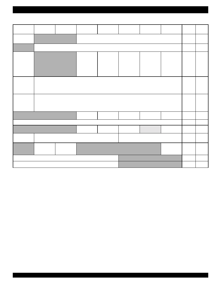
62
RSLIC (IDT82V1671) & CODEC (IDT82V1074) CHIPSET INDUSTRIAL TEMPERATURE RANGE
Table - 23 Coefficient RAM Mapping
Word 7
Word 6
Word 5
Word 4
Word 3
Word 2
Word 1
Word 0
Offset/
Address
Notes
DC Offset
(default value: 0)
Reserved
Impedance Matching Filter (IMF) Coefficient
(default: the IMF is disabled)
00H
Block 0
Reserved
Transhybrid Balance Filter (ECF) Coefficient
(default: the ECF is disabled)
01H
Block 1
Gain for
Impedance
Scaling (GIS)
(default value: 0)
Reserved
Should be
2000H when
using the dual
tone genera-
tors. (default:
0000H)
(1)
Notes:
1. The default value of this word is 0000H. When using the dual tone generators, users should write 2000H (i.e. high byte: 20H, low byte: 00H) to this word to ensure proper operation.
TG2Freq
(default: 1447
Hz)
TG2Amp
(default: 0.94 V)
TG1Freq
(default: 852 Hz)
TG1Amp
(default: 0.94 V)
02H
Block 2
Digital Gain in
Transmit Path
(GTX)
(default: 0 dB)
Coefficient for Frequency Response Correction in Transmit Path (FRX)
(default: the FRX is disabled)
03H
Block 3
Digital Gain in
Receive Path
(GRX)
(default: 0 dB)
Coefficient for Frequency Response Correction in Receive Path (FRR)
(default: the FRR is disabled)
04H
Block 4
Reserved
RampEnd
(default: 20 V)
RampSlope
(default:300V/S)
RingOffset
(default: 7 V)
RingFreq
(default: 30 Hz)
RingAmp
(default: 40 V)
05H
Block 5
DC Feeding Coefficient
06H
Block 6
Reserved
HKHyst
(default: 2 mA)
RTthld_AC
(default: 5 mA)
RTthld_DC
(default: 5 mA)
Reserved
HKthld
(default: 7 mA)
07H
Block 7
UTD Integrator
Coefficient
UTD Bandstop Filter Coefficient
(2)
2. When the gains in the transmit and receive paths are 0 dB, the default parameters of the UTD filters are as follows:
bandpass filter: center frequency is 2100 Hz and bandwidth is 60 Hz.
bandstop filter: center frequency is 2100 Hz and bandwidth is 230 Hz.
UTD Bandpass Filter Coefficient
(2)
08H
Block 8
Reserved
UTDthld_Floor
(default:
-18
dBm)
UTDthld_Ceiling
(default:
-6
dBm)
Reserved
UTD Integrator
Coefficient
09H
Block 9
LM Notch Filter Coefficient
(3)
3. When the gains in the transmit and receive paths are 0 dB, the default parameters of the level meter filter are as follows:
bandpass/notch filter: center frequency is 1014 Hz and quality factor (Q) is 5.
Reserved
0AH
Block 10
LM Bandpass Filter Coefficient
(3)
Reserved
0BH
Block 11

63
RSLIC (IDT82V1671) & CODEC (IDT82V1074) CHIPSET INDUSTRIAL TEMPERATURE RANGE
5.3
REGISTERS DESCRIPTION
5.3.1
REGISTERS OVERVIEW
Table - 24 Global Registers Mapping
Name
Function Description
Register Byte
Read
Command
Write
Command
Default
Value
b7
b6
b5
b4
b3
b2
b1
b0
GREG1
PLL power down
PLL_PD
Reserved
20H
A0H
00H
GREG2
Reserved for future use
Reserved
-
-
-
GREG3
PCM configuration
L_CODE
A/µ
DBL_CLK
TR_SLOPE[1:0]
PCM_OFT[2:0]
22H
A2H
40H
GREG4
MCLK selection and
channel enable
CH_EN[3:0]
MCLK_SEL[3:0]
23H
A3H
02H
GREG5
Hardware/software reset
and version information
HW_RST
Reserved
SW_RST
Reserved
RCH_SEL[3:0]
24H
A4H
00H
GREG6
Loopback control
Reserved
ALB_64K
ALB_8K
ALB_DI
Reserved
DLB_64K
DLB_8K
DLB_DI
25H
A5H
00H
GREG7
Three-party conference
control
Reserved
CONF_EN CONFX_EN
CONF_CS[1:0]
26H
A6H
00H
GREG8
Gain of three-party
conference
G_CONF[7:0]
27H
A7H
00H
GREG9
Transmit highway and time
slot selection for Part B
THS_B
TT_B[6:0]
28H
A8H
00H
GREG10
Receive highway and time
slot selection for Part B
RHS_B
RT_B[6:0]
29H
A9H
00H
GREG11
Transmit highway and time
slot selection for Part C
THS_C
TT_C[6:0]
2AH
AAH
00H
GREG12
Receive highway and time
slot selection for Part C
RHS_C
RT_C[6:0]
2BH
ABH
00H
GREG13
Transmit highway and time
slot selection for Part D
THS_D
TT_D[6:0]
2CH
ACH
00H
GREG14
Receive highway and time
slot selection for Part D
RHS_D
RT_D[6:0]
2DH
ADH
00H
GREG15
Level meter configuration 1
LM_CN[7:0]
2EH
AEH
00H
GREG16
Level meter configuration 2 LM_ONCE
LM_EN
LM_CS[1:0]
Reserved
LM_CN[10:8]
2FH
AFH
00H
GREG17
Level meter result (low)
LMRL[7:0]
30H
-
00H
GREG18
Level meter result (high)
LMRH[7:0]
31H
-
00H
GREG19
FSK flag length
FSK_FL[7:0]
32H
B2H
00H
GREG20
FSK data length
FSK_DL[7:0]
33H
B3H
00H
GREG21
FSK seizure length
FSK_SL[7:0]
34H
B4H
00H
GREG22
FSK mark length
FSK_ML[7:0]
35H
B5H
00H
GREG23
FSK control
Reserved
FSK_CS[1:0]
FSK_EN
FSK_BS
FSK_MAS
FSK_TS
36H
B6H
00H
GREG24
Interrupt polarity
Reserved
INT_POL
Reserved
37H
B7H
00H
GREG25
Reserved for future use
Reserved
-
-
-
GREG26
Off-hook, ground-key
status and interrupt clear
GK[3]
HK[3]
GK[2]
HK[2]
GK[1]
HK[1]
GK[0]
HK[0]
39H
B9H
00H
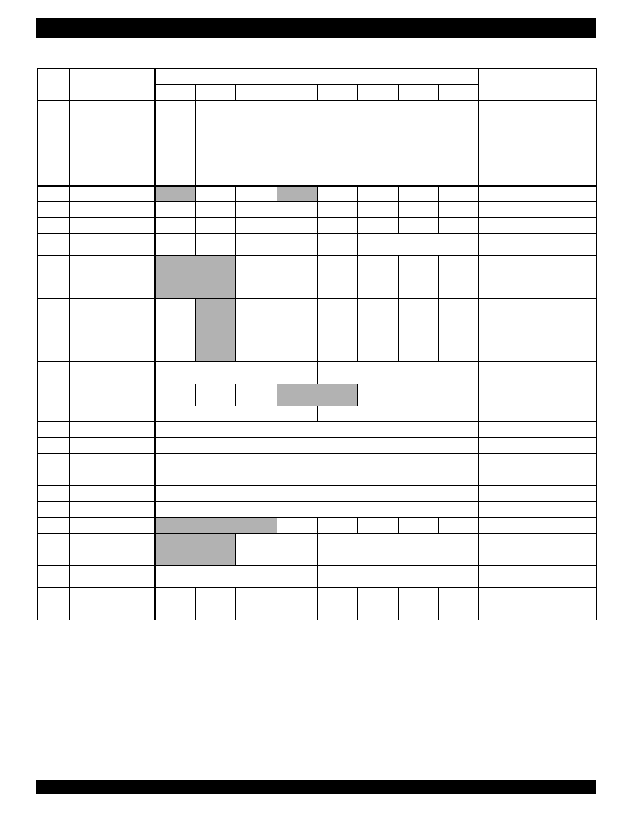
64
RSLIC (IDT82V1671) & CODEC (IDT82V1074) CHIPSET INDUSTRIAL TEMPERATURE RANGE
Table - 25 Local Registers Mapping
Name
Function Description
Register Byte
Read
Command
Write
Command
Default
Value
b7
b6
b5
b4
b3
b2
b1
b0
LREG1
Transmit highway and time
slot selection
THS
TT[6:0]
00H
80H
00H for CH1
01H for CH2
02H for CH3
03H for CH4
LREG2
Receive highway and time
slot selection
RHS
RT[6:0]
01H
81H
00H for CH1
01H for CH2
02H for CH3
03H for CH4
LREG3
Loopback control
Reserved
DLB_2M
DLB_PCM
Reserved ALB_1MDC ALB_2M
ALB_PCM
CUTOFF
02H
82H
00H
LREG4
Coefficient selection
FRR
GRX
FRX
GTX
TG
ECF
IMF
DC_OFT
03H
83H
FFH
LREG5
Coefficient selection
V90
HPF
LM_B
LM_N
UTD
Signaling
DC_FEED
RG
04H
84H
BFH
LREG6
CODEC and RSLIC mode
control
P_DOWN
STANDBY
ACTIVE
RAMP
SCAN_EN
SM[2:0]
05H
85H
80H
LREG7
Analog Gain Selection, AC/
DC Ring Trip Selection,
Ring Generator and Tone
Generators Enable
Reserved
IM_629
RING
RT_SEL
RING_EN
TG2_EN
TG1_EN
06H
86H
00H
LREG8
Ramp Generator Enable,
Level Meter Path Selection
and Notch/Bandpass Filter
Characteristic
Configuration, UTD Source
Selection and UTD Enable
RAMP_EN Reserved LM_NOTCH LM_FILT
LM_SRC
DC_SRC
UTD_SRC
UTD_EN
07H
87H
00H
LREG9
level meter source and
shift factor selection
K[3:0]
LM_SEL[3:0]
08H
88H
00H
LREG10
level meter threshold,
rectifier on/off, gain factor
OTHRE
LM_GF
LM_RECT
Reserved
LM_TH[2:0]
09H
89H
00H
LREG11
Debounce filter
DB[3:0]
DB_IO[3:0]
0AH
8AH
00H
LREG12
PCM data low byte
PCM[7:0]
0BH
-
00H
LREG13
PCM data high byte
PCM[15:8]
0CH
-
00H
LREG14
UTD RTIME
UTD_RT[7:0]
0DH
8DH
13H
LREG15
UTD RBKTime
UTD_RBK[7:0]
0EH
8EH
19H
LREG16
UTD ETIME
UTD_ET[7:0]
0FH
8FH
40H
LREG17
UTD EBRKTime
UTD_EBRK[7:0]
10H
90H
64H
LREG18
Interrupt mask
Reserved
GK_M
HK_M
OTMP_M
RAMP_M
GKP_M
11H
91H
1FH
LREG19
IO interrupt mask, polarity
reverse, external ringing
sync enable
Reserved
REV_POL SYNC_EN
IO_M[3:0]
12H
92H
0FH
LREG20
IO pin direction select and
IO data
IO_C[3:0]
IO[3:0]
13H
93H
00H
LREG21
Interrupt source and DC
feeding characteristic
indication
FEED_I
FEED_V
FEED_R
LM_OK
UTD_OK
OTMP
RAMP_OK
GK_POL
14H
-
01H
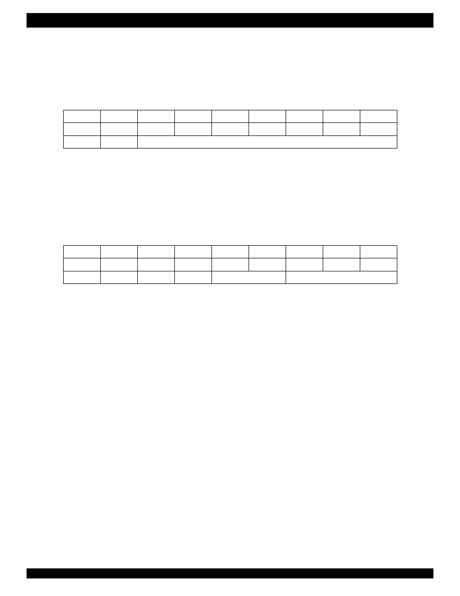
65
RSLIC (IDT82V1671) & CODEC (IDT82V1074) CHIPSET INDUSTRIAL TEMPERATURE RANGE
In the following global registers and local registers lists, it should be noted that:
1. R/W = 0, Read command. R/W = 1, Write command.
2. The reserved bit(s) in the register must be filled in `0' in write operation and will be ignored in read operation.
3. The global or local registers described below are available for both MPI and GCI modes except for those with special statement.
5.3.2
GLOBAL REGISTERS LIST
GREG1: PLL Power Down, Read/Write (20H/A0H)
PLL_PD
Power down the internal PLL block (refer to
"6.2 PLL Power Down" on page 90
for details).
PLL_PD = 0:
the internal PLL block is powered up (default);
PLL_PD = 1:
the internal PLL block is powered down.
Other bits in this register are reserved for future use.
GREG2: Reserved.
This register is reserved for future use.
GREG3: PCM Configuration, Read/Write (22H/A2H)
L_CODE
Voice data code (8-bit, A/µ-law compressed code or 16-bit linear code) selection
L_CODE = 0:
compressed code is selected (default);
L_CODE = 1:
linear code is selected.
A/µ
Select the PCM law
A/µ = 0:
µ-law is selected;
A/µ = 1:
A-law is selected (default).
DBL_CLK
Clock mode (single or double) selection. This bit is used for MPI mode only.
DBL_CLK = 0:
single clock is selected (default);
DBL_CLK = 1:
double clock is selected.
TR_SLOPE[1:0] Transmit and receive slope selection. The TR_SLOPE[1:0] bits are used for MPI mode only.
TR_SLOPE[1:0]=00: transmits data on the rising edges of BCLK, receives data on the falling edges of BCLK (default);
TR_SLOPE[1:0]=01: transmits data on the rising edges of BCLK, receives data on the rising edges of BCLK;
TR_SLOPE[1:0]=10: transmits data on the falling edges of BCLK, receives data on the falling edges of BCLK;
TR_SLOPE[1:0]=11: transmits data on the falling edges of BCLK, receives data on the rising edges of BCLK;
PCM_OFT[2:0]
PCM timing offset selection. The PCM transmit/receive time slot can be offset from FSC by 0 to 7 BCLK periods. The
PCM_OFT[2:0] bits are used for MPI mode only.
PCM_OFT[2:0]=000: offset from FSC by 0 BCLK period (default);
PCM_OFT[2:0]=001: offset from FSC by 1 BCLK period;
PCM_OFT[2:0]=010: offset from FSC by 2 BCLK periods;
PCM_OFT[2:0]=011: offset from FSC by 3 BCLK periods;
PCM_OFT[2:0]=100: offset from FSC by 4 BCLK periods;
PCM_OFT[2:0]=101: offset from FSC by 5 BCLK periods;
PCM_OFT[2:0]=110: offset from FSC by 6 BCLK periods;
PCM_OFT[2:0]=111: offset from FSC by 7 BCLK periods.
b7
b6
b5
b4
b3
b2
b1
b0
Command
R/W
0
1
0
0
0
0
0
I/O data
PLL_PD
Reserved
b7
b6
b5
b4
b3
b2
b1
b0
Command
R/W
0
1
0
0
0
1
0
I/O data
L_CODE
A/
µ
DBL_CLK
TR_SLOPE[1:0]
PCM_OFT[2:0]
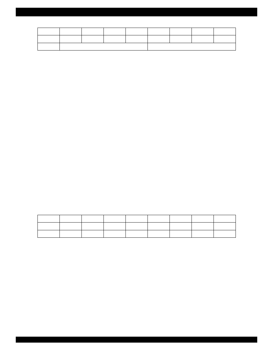
66
RSLIC (IDT82V1671) & CODEC (IDT82V1074) CHIPSET INDUSTRIAL TEMPERATURE RANGE
GREG4: Master Clock Selection and Channel Program Enable, Read/Write (23H/A3H)
CH_EN[3:0]
Channel programming enable. In MPI mode, the channel programming enable command is used to specify the
channel(s) to which the subsequent local command or Coe-RAM command will be applied. The CH_EN[3:0] bits
enable Channel 4 to Channel 1 for programming, respectively. The CH_EN[3:0] bits are used for MPI mode only.
CH_EN[3] = 0:
Disabled, Channel 4 can not receive Local Commands and Coe-RAM Commands (default);
CH_EN[3] = 1:
Enabled, Channel 4 can receive Local Commands and Coe-RAM Commands;
CH_EN[2] = 0:
Disabled, Channel 3 can not receive Local Commands and Coe-RAM Commands (default);
CH_EN[2] = 1:
Enabled, Channel 3 can receive Local Commands and Coe-RAM Commands;
CH_EN[1] = 0:
Disabled, Channel 2 can not receive Local Commands and Coe-RAM Commands (default);
CH_EN[1] = 1:
Enabled, Channel 2 can receive Local Commands and Coe-RAM Commands;
CH_EN[0] = 0:
Disabled, Channel 1 can not receive Local Commands and Coe-RAM Commands (default);
CH_EN[0] = 1:
Enabled, Channel 1 can receive Local Commands and Coe-RAM Commands;
MCLK_SEL[3:0] Select the frequency of the master clock. In MPI mode, there are nine frequencies can be selected as the master
clock. The MCLK_SEL[3:0] bits are used for MPI mode only.
(In GCI mode, the frequency of the master clock is either 2.048 MHz or 4.096 MHz, the same as the frequency of Data
Clock (DCL). The internal circuit of the CODEC monitors the DCL input to determine which frequency is being used.)
MCLK_SEL[3:0] = 0000:
8.192 MHz
MCLK_SEL[3:0] = 0001:
4.096 MHz
MCLK_SEL[3:0] = 0010:
2.048 MHz (default)
MCLK_SEL[3:0] = 0110:
1.536 MHz
MCLK_SEL[3:0] = 1110:
1.544 MHz
MCLK_SEL[3:0] = 0101:
3.072 MHz
MCLK_SEL[3:0] = 1101:
3.088 MHz
MCLK_SEL[3:0] = 0100:
6.144 MHz
MCLK_SEL[3:0] = 1100:
6.176 MHz
GREG5: Hardware and Software Reset, Write (A4H); Version Number, Read (24H)
When write this register, a hardware or a software reset will be applied as described below:
HW_RST
Hardware reset of the CODEC. The action of this hardware reset is equivalent to pulling the RESET pin of the CODEC
low.
HW_RST = 0:
No hardware reset signal will be generated (default);
HW_RST = 1:
A hardware reset signal will be generated.
SW_RST
Software reset of the CODEC. This software reset operation resets those local registers specified by the RCH_SEL[3:0]
bits, but the Coe-RAM is not affected.
SW_RST = 0:
No software reset signal will be generated (default);
SW_RST = 1:
A software reset signal will be generated. If the SW_RST bit is set to 1, those local registers specified
by the RCH_SEL[3:0] bits will be reset, but other local registers and all the global registers as well as
the Coe-RAM will not be affected.
RCH_SEL[3:0] Select channel(s) for software reset. The RCH_SEL[3:0] bits select the local registers of Channel 4 to Channel 1,
respectively, to be reset.
RCH_SEL[3] = 0: The local registers of Channel 4 will not be reset after executing a software reset command (default));
RCH_SEL[3] = 1: The local registers of Channel 4 will be reset after executing a software reset command;
b7
b6
b5
b4
b3
b2
b1
b0
Command
R/W
0
1
0
0
0
1
1
I/O data
CH_EN[3:0]
MCLK_SEL[3:0]
b7
b6
b5
b4
b3
b2
b1
b0
Command
R/W
0
1
0
0
1
0
0
I/O data
HW_RST
Reserved
SW_RST
Reserved
RCH_SEL[3] RCH_SEL[2] RCH_SEL[1] RCH_SEL[0]

67
RSLIC (IDT82V1671) & CODEC (IDT82V1074) CHIPSET INDUSTRIAL TEMPERATURE RANGE
RCH_SEL[2] = 0: The local registers of Channel 3 will not be reset after executing a software reset command (default));
RCH_SEL[2] = 1: The local registers of Channel 3 will be reset after executing a software reset command;
RCH_SEL[1] = 0: The local registers of Channel 2 will not be reset after executing a software reset command (default);
RCH_SEL[1] = 1: The local registers of Channel 2 will be reset after executing a software reset command;
RCH_SEL[0] = 0: The local registers of Channel 1 will not be reset after executing a software reset command (default);
RCH_SEL[0] = 1: The local registers of Channel 1 will be reset after executing a software reset command;
When read this register, the CODEC version number of 5AH will be read out.
GREG6: Test Loopback Control, Read/Write (25H/A5H)
This register is used to enable the analog and digital loopbacks for testing.
ALB_64K
Analog loopback via 64 KHz
ALB_64K = 0:
ALB_64K loopback is disabled (normal operation) (default);
ALB_64K = 1:
ALB_64K loopback is enabled.
ALB_8K
Analog loopback via 8 KHz
ALB_8K = 0:
ALB_8K loopback is disabled (normal operation) (default);
ALB_8K = 1:
ALB_8K loopback is enabled.
ALB_DI
Analog loopback via DX to DR (This loopback is available for MPI mode only)
ALB_DI = 0:
ALB_DI loopback is disabled (normal operation) (default);
ALB_DI = 1:
ALB_DI loopback is enabled.
DLB_64K
Digital loopback via 64 KHz
DLB_64K = 0:
DLB_64K loopback is disabled (normal operation) (default);
DLB_64K = 1:
DLB_64K loopback is enabled.
DLB_8K
Digital loopback via 8 KHz
DLB_8K = 0:
DLB_8K loopback is disabled (normal operation) (default);
DLB_8K = 1:
DLB_8K loopback is enabled.
DLB_DI
Digital loopback via DR to DX (This loopback is available for MPI mode only)
DLB_DI = 0:
DLB_DI loopback is disabled (normal operation) (default);
DLB_DI = 1:
DLB_DI loopback is enabled.
GREG7: Three-Party Conference Configuration, Read/Write (26H/A6H)
CONF_EN
Enable internal three-party conference
CONF_EN = 0:
Internal conference is disabled (default);
CONF_EN = 1:
Internal conference is enabled.
CONFX_EN
Enable external three-party conference
CONFX_EN = 0: External conference is disabled (default);
CONFX_EN = 1: External conference is enabled.
CONF_CS[1:0] Select a channel for three-party conference
CONF_CS[1:0] = 00: Channel 1 is selected (default);
b7
b6
b5
b4
b3
b2
b1
b0
Command
R/W
0
1
0
0
1
0
1
I/O data
Reserved
ALB_64K
ALB_8K
ALB_DI
Reserved
DLB_64K
DLB_8K
DLB_DI
b7
b6
b5
b4
b3
b2
b1
b0
Command
R/W
0
1
0
0
1
1
0
I/O data
Reserved
CONF_EN
CONFX_EN
CONF_CS[1:0]

68
RSLIC (IDT82V1671) & CODEC (IDT82V1074) CHIPSET INDUSTRIAL TEMPERATURE RANGE
CONF_CS[1:0] = 01: Channel 2 is selected;
CONF_CS[1:0] = 10: Channel 3 is selected;
CONF_CS[1:0] = 11: Channel 4 is selected.
GREG8: Three-Party Conference Gain Setting, Read/Write (27H/A7H)
G_CONF[7:0] Gain of three-party conference. The gain is calculated by the following formula:
Gain = G_CONF[7:0] / 256
The default value of G_CONG[7:0] bits is 0(d).
GREG9: Transmit Time Slot and Highway Selection for Part B in Three-Party Conference, Read/Write (28H/A8H)
THS_B
Transmit PCM highway selection for part B in three-party conference
THS_B = 0:
transmit PCM highway one (DX1) is selected (default);
THS_B = 1:
transmit PCM highway two (DX2) is selected.
TT_B[6:0]
Transmit time slot selection for part B in three-party conference.
The valid value of the TT_B[6:0] bits is from 0(d) to 127(d), corresponding to Time Slot 0 to Time Slot 127.
The default value of TT_B[6:0] is 0(d).
GREG10: Receive Time Slot and Highway Selection for Part B in Three Party Conference, Read/Write (29H/A9H)
RHS_B
Receive PCM highway selection for part B in three-party conference
RHS_B = 0:
receive PCM highway one (DR1) is selected (default);
RHS_B = 1:
receive PCM highway two (DR2) is selected.
RT_B[6:0]
Receive PCM time slot selection for part B in three-party conference.
The valid value of the RT_B[6:0] bits is from 0(d) to 127(d), corresponding to Time Slot 0 to Time Slot 127.
The default value of RT_B[6:0] is 0(d).
GREG11: Transmit Time Slot and Highway Selection for Part C in Three-Party Conference, Read/Write (2AH/AAH)
THS_C
Transmit PCM highway selection for part C in three-party conference
THS_C = 0:
transmit PCM highway one (DX1) is selected (default);
THS_C = 1:
transmit PCM highway two (DX2) is selected.
TT_C[6:0]
Transmit time slot selection for part C in three-party conference.
The valid value of the TT_C[6:0] bits is from 0(d) to 127(d), corresponding to Time Slot 0 to Time Slot 127.
The default value of TT_C[6:0] is 0(d).
b7
b6
b5
b4
b3
b2
b1
b0
Command
R/W
0
1
0
0
1
1
1
I/O data
G_CONF[7:0]
b7
b6
b5
b4
b3
b2
b1
b0
Command
R/W
0
1
0
1
0
0
0
I/O data
THS_B
TT_B[6:0]
b7
b6
b5
b4
b3
b2
b1
b0
Command
R/W
0
1
0
1
0
0
1
I/O data
RHS_B
RT_B[6:0]
b7
b6
b5
b4
b3
b2
b1
b0
Command
R/W
0
1
0
1
0
1
0
I/O data
THS_C
TT_C[6:0]

69
RSLIC (IDT82V1671) & CODEC (IDT82V1074) CHIPSET INDUSTRIAL TEMPERATURE RANGE
GREG12: Receive Time Slot and Highway Selection for Part C in Three-Party Conference, Read/Write (2BH/ABH)
RHS_C
Receive PCM highway selection for part C in three-party conference
RHS_C = 0:
receive PCM highway one (DR1) is selected (default);
RHS_C = 1:
receive PCM highway two (DR2) is selected.
RT_C[6:0]
Receive time slot selection for part C in three-party conference.
The valid value of the RT_C[6:0] bits is from 0(d) to 127(d), corresponding to Time Slot 0 to Time Slot 127.
The default value of RT_C[6:0] is 0(d).
GREG13: Transmit Time Slot and Highway Selection for Part D in Three-Party Conference, Read/Write (2CH/ACH)
THS_D
Transmit PCM highway selection for part D in three-party conference
THS_D = 0:
transmit PCM highway one (DX1) is selected (default);
THS_D = 1:
transmit PCM highway two (DX2) is selected.
TT_D[6:0]
Transmit time slot selection for part D in three-party conference.
The valid value of the TT_D[6:0] bits is from 0(d) to 127(d), corresponding to Time Slot 0 to Time Slot 127.
The default value of TT_D[6:0] is 0(d).
GREG14: Receive Time Slot and Highway Selection for Part D in Three-Party Conference, Read/Write (2DH/ADH)
RHS_D
Receive PCM highway selection for part D in three-party conference
RHS_D = 0:
receive PCM highway one (DR1) is selected (default);
RHS_D = 1:
receive PCM highway two (DR2) is selected.
RT_D[6:0]
Receive time slot selection for part D in three-party conference.
The valid value of the RT_D[6:0] bits is from 0(d) to 127(d), corresponding to Time Slot 0 to Time Slot 127.
The default value of RT_D[6:0] is 0(d).
GREG15: Level Meter Count_Number Low 8 bits, Read/Write (2EH/AEH)
The LM_CN[7:0] bits in this register together with the LM_CN[10:8] bits in GREG16 form an 11-bit counter register, which is used for the
level meter to set the time period for PCM data sampling.
The maximum number of time cycles set by the LM_CN[10:0] bits is 7FFH, corresponding to 255.875 ms. The time period for sampling
can be programmed from 0 ms to 255.875 ms in steps of 0.125 ms (8k). If the LM_CN[10:0] bits are set to be 000H (corresponding to 0
ms), the PCM data will be transmitted transparently to the level meter result registers without being sampled.
LM_CN[10:0] = 0 (d): The PCM data is transmitted to level meter result registers GREG17 and GREG18 directly (default);
LM_CN[10:0] = N (d):The PCM data is sampled for N
125 µs (N from 1 to 2047).
b7
b6
b5
b4
b3
b2
b1
b0
Command
R/W
0
1
0
1
0
1
1
I/O data
RHS_C
RT_C[6:0]
b7
b6
b5
b4
b3
b2
b1
b0
Command
R/W
0
1
0
1
1
0
0
I/O data
THS_D
TT_D[6:0]
b7
b6
b5
b4
b3
b2
b1
b0
Command
R/W
0
1
0
1
1
0
1
I/O data
RHS_D
RT_D[6:0]
b7
b6
b5
b4
b3
b2
b1
b0
Command
R/W
0
1
0
1
1
1
0
I/O data
LM_CN[7:0]

70
RSLIC (IDT82V1671) & CODEC (IDT82V1074) CHIPSET INDUSTRIAL TEMPERATURE RANGE
GREG16: Level Meter Count_Number High 3 bits; Level Meter On/Off, Channel Selection and Once/Continuous Measurement, Read/Write
(2FH/AFH)
LM_ONCE
Execution mode of the integrator in level meter. The integration can be executed continuously or once after every initia-
tion.
LM_ONCE = 0:
The integrator runs continuously (default);
LM_ONCE = 1:
The integrator runs only once. To start again, the LM_EN bit must be set from 0 to 1 again.
LM_EN
Level meter function enable. This bit starts or stops level metering.
LM_EN = 0:
disabled, level metering stops (default);
LM_EN = 1:
enabled, level metering starts.
LM_CS
Level meter channel selection. The LM_CS[1:0] bits determine the data on which channel will be level metered.
LM_CS[1:0] = 00: The data on Channel 1 will be input to the level meter (default);
LM_CS[1:0] = 01: The data on Channel 2 will be input to the level meter;
LM_CS[1:0] = 10: The data on Channel 3 will be input to the level meter;
LM_CS[1:0] = 11: The data on Channel 4 will be input to the level meter.
LM_CN
Level meter count number high 3 bits LM_CN[10:8]. Refer to the description of GREG15 for details.
GREG17: Level Meter Result Register (Low), Read Only (30H)
This register contains the low byte of the level meter result. The default value of LMRL[7:0] bits is 0.
GREG18: Level Meter Result Register (High), Read Only (31H)
This register contains the high byte of the level meter result. The default value of the LMRH[7:0] is 0.
GREG19: FSK Flag Length Register, Read/Write (32H/B2H)
The flag signal is a stream of '1'. It is transmitted between two message bytes during the Caller ID data transmission.
This register is used to set the number of the flag bits '1'. The value of FSK_FL[7:0] bits is valid from 0 to 255(d).
The default value of 0(d) means that no flag signal will be sent out.
GREG20: FSK Data Length Register, Read/Write (33H/B3H)
This register is used to set the length of the data bytes that will be transmitted except the flag signal.
The value of the FSK_DL[7:0] bits is valid from 0 to 64(d). Any value larger than 64(d) will be taken as 64(d) by the DSP.
b7
b6
b5
b4
b3
b2
b1
b0
Command
R/W
0
1
0
1
1
1
1
I/O data
LM_ONCE
LM_EN
LM_CS
LM_CS[0]
Reserved
LM_CN[10:8]
b7
b6
b5
b4
b3
b2
b1
b0
Command
0
0
1
1
0
0
0
0
I/O data
LMRL[7:0]
b7
b6
b5
b4
b3
b2
b1
b0
Command
0
0
1
1
0
0
0
1
I/O data
LMRH[7:0]
b7
b6
b5
b4
b3
b2
b1
b0
Command
R/W
0
1
1
0
0
1
0
I/O data
FSK_FL[7:0]
b7
b6
b5
b4
b3
b2
b1
b0
Command
R/W
0
1
1
0
0
1
1
I/O data
FSK_DL[7:0]
71
RSLIC (IDT82V1671) & CODEC (IDT82V1074) CHIPSET INDUSTRIAL TEMPERATURE RANGE
The default value of 0 means that no data bytes will be sent out.
GREG21: FSK Seizure Length Register, Read/Write (34H/B4H)
The seizure length is the number of '01' pairs that represent the seizure phase.
The seizure length is two times of the value of the FSK_SL[7:0] bits. The value of the FSK_SL[7:0] bits is valid from 0 to 255(d), corre-
sponding to the seizure length from 0 to 510 (d).
The default value of this register is 0, that means no seizure signal will be sent out.
GREG22: FSK Mark Length Register, Read/Write (35H/B5H)
The mark signal is a stream of '1' that will be transmitted in initial flag phase.
This register is used to set the number of the mark bits `1'. The value of the FSK_ML[7:0] bits is valid from 0 to 255(d).
The default value of 0 means that no mark signal will be sent out.
GREG23: FSK Transmit Start, Mark_after_send, Modulation Standard, FSK Channel Selection, FSK enable, Read/Write (36H/B6H)
FSK_CS
FSK channel selection. The FSK_CS[1:0] bits select a channel on which the FSK signal is generated.
FSK_CS[1:0] = 00: Channel 1 is selected (default);
FSK_CS[1:0] = 01: Channel 2 is selected;
FSK_CS[1:0] = 10: Channel 3 is selected;
FSK_CS[1:0] = 11: Channel 4 is selected.
FSK_EN
FSK function block enable.
FSK_EN = 0:
FSK function block is disabled (default);
FSK_EN = 1:
FSK function block is enabled.
FSK_BS
FSK modulation standard selection
FSK_BS = 0:
BELL 202 standard is selected (default);
FSK_BS = 1:
ITU-T V.23 standard is selected.
FSK_MAS
Mark After Send. The FSK_MAS bit determines whether the FSK generator will keep on sending a mark-after-send sig-
nal (a string of `1') after finish sending the data in the FSK-RAM.
FSK_MAS = 0:
The FSK output will be muted after sending out the data in the FSK-RAM (default);
FSK_MAS = 1:
The FSK generator sends out a mark-after-send signal after finish sending out the data in the FSK-
RAM. This signal will be stopped if the FSK_MAS bit is set to 0.
FSK_TS
FSK transmission starts.
FSK_TS = 0:
FSK transmission is disabled (default);
FSK_TS = 1:
FSK transmission starts.
The FSK_TS bit will be reset automatically after the data in the FSK-RAM is finished sending. If the
seizure length, the mark length and the data length are set to 0, the FSK_TS bit will be reset to 0
immediately after it is set to 1.
b7
b6
b5
b4
b3
b2
b1
b0
Command
R/W
0
1
1
0
1
0
0
I/O data
FSK_SL[7:0]
b7
b6
b5
b4
b3
b2
b1
b0
Command
R/W
0
1
1
0
1
0
1
I/O data
FSK_ML[7:0]
b7
b6
b5
b4
b3
b2
b1
b0
Command
R/W
0
1
1
0
1
1
0
I/O data
Reserved
FSK_CS[1:0]
FSK_EN
FSK_BS
FSK_MAS
FSK_TS

72
RSLIC (IDT82V1671) & CODEC (IDT82V1074) CHIPSET INDUSTRIAL TEMPERATURE RANGE
GREG24: Interrupt Polarity Selection Register, Read/Write (37H/B7H)
INT_POL
Interrupt polarity selection. The INT_POL bit determines the valid polarity of all the interrupt signals including the
INT_CHA and INT_CHB bits in GCI C/I channel.
INT_POL = 0:
Active low (default);
INT_POL = 1:
Active high.
GREG25: Reserved
This register is reserved for future use.
GREG26: RSLIC Status, Read (39H); Interrupt Clear, Write (B9H)
In MPI mode, when applying a read operation to this register, the off-hook and ground-key status of all four channels will be read out. If
an interrupt caused by off-hook or ground-key detection is pending, reading this register will clear the interrupt.
HK[3:0]
Off-hook status.
HK[0] = 0:
Channel 1 is on-hook (default);
HK[0] = 1:
Channel 1 is off-hook.
HK[1] = 0:
Channel 2 is on-hook (default);
HK[1] = 1:
Channel 2 is off-hook.
HK[2] = 0:
Channel 3 is on-hook (default);
HK[2] = 1:
Channel 3 is off-hook.
HK[3] = 0:
Channel 4 is on-hook (default);
HK[3] = 1:
Channel 4 is off-hook.
GK[3:0]
ground-key status.
GK[0] = 0:
No longitudinal current detected on Channel 1 (default);
GK[0] = 1:
Longitudinal current detected (ground-key or ground start) on Channel 1;
GK[1] = 0:
No longitudinal current detected on Channel 2 (default);
GK[1] = 1:
Longitudinal current detected (ground-key or ground start) on Channel 2;
GK[2] = 0:
No longitudinal current detected on Channel 3 (default);
GK[2] = 1:
Longitudinal current detected (ground-key or ground start) on Channel 3;
GK[3] = 0:
No longitudinal current detected on Channel 4 (default);
GK[3] = 1:
Longitudinal current detected (ground-key or ground start) on Channel 4;
In GCI mode, the off-hook and ground-key status are reported via the upstream C/I channel only. Reading this register will always get a
result of 00H. If an interrupt caused by off-hook or ground-key detection is pending, applying a read command to this register will clear
the interrupt.
In both MPI and GCI modes, when applying a write operation to this register, all the interrupts will be cleared.
b7
b6
b5
b4
b3
b2
b1
b0
Command
R/W
0
1
1
0
1
1
1
I/O data
Reserved
INT_POL
Reserved
b7
b6
b5
b4
b3
b2
b1
b0
Command
R/W
0
1
1
1
0
0
1
I/O data
GK[3]
HK[3]
GK[2]
HK[2]
GK[1]
HK[1]
GK[0]
HK[0]

73
RSLIC (IDT82V1671) & CODEC (IDT82V1074) CHIPSET INDUSTRIAL TEMPERATURE RANGE
5.3.3
LOCAL REGISTERS LIST
LREG1: Transmit Time Slot and Transmit Highway Selection, Read/Write (00H/80H). This register is used for MPI mode only.
THS
Transmit PCM highway selection for the specified channel.
THS = 0:
transmit PCM highway one (DX1) is selected (default);
THS = 1:
transmit PCM highway two (DX2) is selected.
TT[6:0]
Transmit time slot selection for the specified channel.
The valid value of the TT[6:0] bits is from 0(d) to 127(d), corresponding to Time Slot 0 to Time Slot 127.
The default value of TT[6:0] is 00H for Channel 1, 01H for Channel 2, 02H for Channel 3 and 03H for Channel 4.
LREG2: Receive Time Slot and Receive Highway Selection, Read/Write (01H/81H). This register is used for MPI mode only.
RHS
Receive PCM highway selection for the specified channel.
RHS = 0:
receive PCM highway one (DR1) is selected (default);
RHS = 1:
receive PCM highway two (DR2) is selected.
RT[6:0]
Receive time slot selection for the specified channel.
The valid value of the RT[6:0] bits is from 0(d) to 127(d), corresponding to Time Slot 0 to Time Slot 127.
The default value of RT[6:0] is 00H for Channel 1, 01H for Channel 2, 02H for Channel 3 and 03H for Channel 4.
LREG3: Loopback Control, Read/Write (02H/82H)
The register is used to enable the digital and analog loopbacks on the specified channel(s) for testing.
DLB_2M
Digital loopback via 2M
DLB_2M = 0:
disabled (normal operation) (default);
DLB_2M = 1:
enabled (closed);
DLB_PCM
Digital loopback via the PCM interface (This loopback is available for MPI mode only)
DLB_PCM = 0:
disabled (normal operation) (default);
DLB_PCM = 1:
enabled (closed);
ALB_1MDC
Analog loopback via 1M in the DC loop
ALB_1MDC = 0: disabled (normal operation) (default);
ALB_1MDC = 1: enabled (closed);
ALB_2M
Analog loopback via 2M
ALB_2M = 0:
disabled (normal operation) (default);
ALB_2M = 1:
enabled (closed);
ALB_PCM
Analog loopback via the PCM interface (This loopback is available for MPI mode only)
ALB_PCM = 0:
disabled (normal operation) (default);
ALB_PCM = 1:
enabled (closed);
CUTOFF
Cut off PCM receive path
b7
b6
b5
b4
b3
b2
b1
b0
Command
R/W
0
0
0
0
0
0
0
I/O data
THS
TT[6:0]
b7
b6
b5
b4
b3
b2
b1
b0
Command
R/W
0
0
0
0
0
0
1
I/O data
RHS
RT[6:0]
b7
b6
b5
b4
b3
b2
b1
b0
Command
R/W
0
0
0
0
0
1
0
I/O data
Reserved
DLB_2M
DLB_PCM
Reserved
ALB_1MDC
ALB_2M
ALB_PCM
CUTOFF

74
RSLIC (IDT82V1671) & CODEC (IDT82V1074) CHIPSET INDUSTRIAL TEMPERATURE RANGE
CUTOFF = 0:
disabled, the PCM receive path is in normal operation (default);
CUTOFF = 1:
enabled, the PCM receive path is cut off.
LREG4: Coefficient Selection, Read/Write (03H/83H)
This register determines whether the default values or the coefficients in Coe-RAM is selected for the programmable filters, tone genera-
tors and DC offset compensation.
FRR
Coefficient selection for the Frequency Response correction in the Receive path
FRR = 0:
coefficient in the Coe-RAM is selected;
FRR = 1:
the frequency response correction in the receive path is disabled (default).
GRX
Coefficient selection for the digital Gain filter in the Receive path
GRX = 0:
coefficient in the Coe-RAM is selected;
GRX = 1:
the digital gain in the receive path is 0 dB (default).
FRX
Coefficient selection for the Frequency Response correction in the Transmit path
FRX = 0:
coefficient in the Coe-RAM is selected;
FRX = 1:
the frequency response correction in the transmit path is disabled (default).
GTX
Coefficient selection for the digital Gain filter in the Transmit path
GTX = 0:
coefficient in the Coe-RAM is selected;
GTX = 1:
the digital gain in the transmit path is 0 dB (default).
TG
Coefficient selection for the Tone Generators (TG1 and TG2)
TG = 0:
coefficient in the Coe-RAM is selected;
TG = 1:
coefficient in the ROM is selected (default)
(The default values are: TG1Amp = 0.94 V, TG1Freq = 852 Hz, TG2Amp = 0.94 V, TG2Freq = 1447
Hz).
ECF
Coefficient selection for the Echo Cancellation filter
ECF = 0:
coefficient in the Coe-RAM is selected;
ECF = 1:
the echo cancellation filter is disabled (default).
IMF
Coefficient selection for the Impedance Matching filter
IMF = 0:
coefficient in the Coe-RAM is selected;
IMF = 1:
the impedance matching filter is disabled (default).
DC_OFT
Compensation value selection for the Offset Register
DC_OFT = 0:
the compensation value in the Coe-RAM is used;
DC_OFT = 1:
the DC offset compensation value in the ROM (which is 0) is used (default).
LREG5: Coefficient Selection and Filter Control Register, Read/Write (04H/84H)
V90
V90 filter characteristic enable. The bit is used to select the filter characteristic of the lowpass filter in voice signal path.
The V90 filter characteristic may be selected for a modem transmission to improve the transmission rate and
performance.
V90 = 0:
The V90 filter is enabled;
V90 = 1:
The V90 filter is disabled (default);.
HPF
Enable/disable the highpass filter
b7
b6
b5
b4
b3
b2
b1
b0
Command
R/W
0
0
0
0
0
1
1
I/O data
FRR
GRX
FRX
GTX
TG
ECF
IMF
DC_OFT
b7
b6
b5
b4
b3
b2
b1
b0
Command
R/W
0
0
0
0
1
0
0
I/O data
V90
HPF
LM_B
LM_N
UTD
Signaling
DC_FEED
RG
75
RSLIC (IDT82V1671) & CODEC (IDT82V1074) CHIPSET INDUSTRIAL TEMPERATURE RANGE
HPF = 0:
The highpass filter is enabled (default);
HPF = 1:
The highpass filter is disabled.
LM_B
Coefficient selection for the level meter bandpass filter
LM_B = 0:
coefficient in the Coe-RAM is used for the level meter bandpass filter;
LM_B = 1:
coefficient in the ROM is used for the level meter bandpass filter (default).
LM_N
Coefficient selection for the level meter notch filter
LM_N = 0:
coefficient in the Coe-RAM is used for the level meter notch filter;
LM_N = 1:
coefficient in the ROM is used for the level meter notch filter (default).
UTD
Coefficient and threshold selection for the UTD
UTD = 0:
coefficient and threshold in the Coe-RAM are used for UTD;
UTD = 1:
coefficient and threshold in the ROM are used for UTD (default).
Signaling
Coefficient selection for signaling (thresholds for off-hook, ground-key and ring trip detection)
Signaling = 0:
coefficients in the Coe-RAM are used;
Signaling = 1:
coefficients in the ROM are used (refer to
Table - 23 on page 62
for details) (default).
DC_FEED
Coefficient selection for DC feeding characteristic
DC_FEED = 0:
coefficient in the Coe-RAM is used;
DC_FEED = 1:
coefficient in the ROM is used (default).
RG
Coefficients selection for Ring Generator and Ramp Generator
RG = 0:
coefficient in the Coe-RAM is used;
RG = 1:
coefficient in the ROM is used (default).
LREG6: CODEC and RSLIC Mode Control Register, Read/Write (05H/85H)
All eight bits in this register and the RING bit in LREG7 are used to control the operating mode of the chipset.
The higher four bits in this register and the RING bit in LREG7 are used to control the operating mode of the CODEC.
P_DOWN = 0:
power down mode is disabled;
P_DOWN = 1:
power down mode is enabled (default).
STANDBY = 0:
standby mode is disabled (default);
STANDBY = 1:
standby mode is enabled.
ACTIVE = 0:
active mode is disabled (default);
ACTIVE = 1:
active mode is enabled.
RAMP = 0:
ramp mode is disabled (default);
RAMP = 1:
ramp mode is enabled;
The lower four bits in this register are used to control the operating mode of the RSLIC. These four bits are used for MPI mode only.
(In GCI mode, the SCAN_EN and SM[2:0] bits in the downstream C/I channel byte control the operating mode of the RSLIC. Refer to
"4.2.3.1 Downstream C/I Channel Byte" on page 55
for details)
SCAN_EN = 0:
the corresponding RSLIC will not be accessed (default);
SCAN_EN = 1:
the corresponding RSLIC will be accessed.
The SM[2:0] bits determine the operating mode of the RSLIC as shown in the following:
SM[2:0] = '000':
Normal Active mode (default);
SM[2:0] = '001':
External Ring;
SM[2:0] = '010':
Internal Ring;
b7
b6
b5
b4
b3
b2
b1
b0
Command
R/W
0
0
0
0
1
0
1
I/O data
P_DOWN
STANDBY
ACTIVE
RAMP
SCAN_EN
SM[2:0]

76
RSLIC (IDT82V1671) & CODEC (IDT82V1074) CHIPSET INDUSTRIAL TEMPERATURE RANGE
SM[2:0] = '011':
Ring Open;
SM[2:0] = '100':
Tip Open;
SM[2:0] = '101':
Internal Test;
SM[2:0] = '110':
Low Power Standby;
SM[2:0] = '111':
Power Down.
LREG7: Analog Gain Selection, AC/DC Ring Trip Selection, Ring Generator and Tone Generators Enable, Read/Write (06H/86H)
IM_629
Analog Gain for Impedance Scaling (AGIS)
IM_629 = 0:
600
(only for loops with 600 equivalent impedance) (default);
IM_629 = 1:
900
(for all loops including those with 600 equivalent impedance).
RING
CODEC operating mode control bit
RING = 0:
Ring mode is disabled (default);
RING = 1:
Ring mode is enabled.
RT_SEL
AC/DC ring trip selection
RT_SEL = 0:
AC Ring Trip is selected (default);
RT_SEL = 1:
DC Ring Trip is selected.
RING_EN
Enable the internal ring generator
RING_EN = 0:
internal ringing stops (default);
RING_EN = 1:
internal ringing starts.
TG2_EN
Enable Tone Generator 2 (TG2)
TG2_EN = 0:
TG2 is disabled (default);
TG2_EN = 1:
TG2 is enabled.
TG1_EN
Enable Tone Generator 1 (TG1)
TG1_EN = 0:
TG1 is disabled (default);
TG1_EN = 1:
TG1 is enabled.
LREG8: Ramp Generator Enable, Level Meter Path Selection and Notch/Bandpass Filter Characteristic Configuration, UTD Source
Selection and UTD Enable, Read/Write (07H/87H)
RAMP_EN
Enable Ramp Generator
RAMP_EN = 0:
ramp generator is disabled (default);
RAMP_EN = 1:
ramp generator is enabled.
LM_NOTCH
Level meter notch/bandpass filter characteristic selection
LM_NOTCH = 0: notch filter characteristic is selected (default);
LM_NOTCH = 1: bandpass filter characteristic is selected.
LM_FILT
Level meter filter (bandpass/notch) enable
LM_FILT = 0:
level meter filter (bandpass/notch) is disabled (default);
LM_FILT = 1:
level meter filter (bandpass/notch) is enabled.
LM_SRC
Level meter AC/DC source selection
LM_SRC = 0:
signal from DC path is selected for level metering (default);
LM_SRC = 1:
signal from AC path is selected for level metering.
b7
b6
b5
b4
b3
b2
b1
b0
Command
R/W
0
0
0
0
1
1
0
I/O data
Reserved
IM_629
RING
RT_SEL
RING_EN
TG2_EN
TG1_EN
b7
b6
b5
b4
b3
b2
b1
b0
Command
R/W
0
0
0
0
1
1
1
I/O data
RAMP_EN
Reserved
LM_NOTCH
LM_FILT
LM_SRC
DC_SRC
UTD_SRC
UTD_EN

77
RSLIC (IDT82V1671) & CODEC (IDT82V1074) CHIPSET INDUSTRIAL TEMPERATURE RANGE
DC_SRC
DC transmit/receive path selection for level meter
DC_SRC = 0:
signal from DC receive path is selected for level metering (default);
DC_SRC = 1:
signal from DC transmit path is selected for level metering.
UTD_SRC
UTD source selection
UTD_SRC = 0:
signal from receive path is detected by the UTD unit (default);
UTD_SRC = 1:
signal from transmit path is detected by the UTD unit.
UTD_EN
Enable the universal tone detection unit
UTD_EN = 0:
the UTD unit is disabled (default);
UTD_EN = 1:
the UTD unit is enabled.
LREG9: Level Meter Source and Shift Factor Selection, Read/Write (08H/88H)
K[3:0]
Shift factor selection for the level meter.
K[3:0] = 0000:
K
INT
= 1 (default);
K[3:0] = 0001:
K
INT
= 1/2;
K[3:0] = 0010:
K
INT
= 1/4;
K[3:0] = 0011:
K
INT
= 1/8;
K[3:0] = 0100:
K
INT
= 1/16;
K[3:0] = 0101:
K
INT
= 1/32;
K[3:0] = 0110:
K
INT
= 1/64;
K[3:0] = 0111:
K
INT
= 1/128;
K[3:0] = 1000:
K
INT
= 1/256;
K[3:0] = 1001:
K
INT
= 1/512;
K[3:0] = 1010:
K
INT
= 1/1024;
K[3:0] = 1011 to 1111: K
INT
= 1/2048;
LM_SEL[3:0]
Source selection for DC Level Meter
LM_SEL[3:0] = 0000: DC voltage on VTDC is selected (default);
LM_SEL[3:0] = 0100: DC out voltage on DCN-DCP is selected;
LM_SEL[3:0] = 1001: DC voltage on VL is selected;
LM_SEL[3:0] = 1010: Voltage on IO3 is selected;
LM_SEL[3:0] = 1011: Voltage on IO4 is selected;
LM_SEL[3:0] = 1100: Voltage on RTIN is selected;
LM_SEL[3:0] = 1101: VDD/2 is selected;
LM_SEL[3:0] = 1110: VCM (offset of encoding) is selected;
LM_SEL[3:0] = 1111: Voltage on IO4-IO3 is selected;
LREG10: Level Meter Threshold, Rectifier On/Off, Gain Factor, Read/Write (09H/89H)
OTHRE
Over threshold indication for level meter. This bit is read only.
OTHRE = 0:
The level meter result is below the threshold (default);
OTHRE = 1:
The level meter result is over the threshold.
LM_GF
Additional Gain Factor for level meter
LM_GF = 0:
No additional gain factor is selected (default);
LM_GF = 1:
Additional gain factor of 16 is selected.
b7
b6
b5
b4
b3
b2
b1
b0
Command
R/W
0
0
0
1
0
0
0
I/O data
K[3:0]
LM_SEL[3:0]
b7
b6
b5
b4
b3
b2
b1
b0
Command
R/W
0
0
0
1
0
0
1
I/O data
OTHRE
LM_GF
LM_RECT
Reserved
LM_TH[2:0]
78
RSLIC (IDT82V1671) & CODEC (IDT82V1074) CHIPSET INDUSTRIAL TEMPERATURE RANGE
LM_RECT
Enable the rectifier in the level meter.
LM_RECT = 0:
The rectifier is disabled (default);
LM_RECT = 1:
The rectifier is enabled.
LM_TH[2:0]
Level meter threshold selection. If the absolute value of the level meter result exceeds the selected threshold, the
OTHRE bit will be set to 1.
LM_TH[2:0] = 000: Threshold is 0.0% (default);
LM_TH[2:0] = 001: Threshold is 12.5%;
LM_TH[2:0] = 010: Threshold is 25.0%;
LM_TH[2:0] = 011: Threshold is 37.5%;
LM_TH[2:0] = 100: Threshold is 50.0%;
LM_TH[2:0] = 101: Threshold is 62.5%;
LM_TH[2:0] = 110: Threshold is 75.0%;
LM_TH[2:0] = 111: Threshold is 87.5%.
LREG11: Debounce Filter Configuration, Read/Write (0AH/8AH)
DB[3:0]
Debounce interval selection for off-hook and ground-key detection. The debounce interval is programmable from 0.125
ms to 2 ms in steps of 0.125 ms, corresponding to the minimal debounce time of from 2 ms to 30 ms.
DB[3:0] = 0000:
the debounce interval is 0.125 ms, the minimal debounce time is 2 ms (default);
DB[3:0] = 0001:
the debounce interval is 0.250 ms, the minimal debounce time is 4 ms;
DB[3:0] = 0010:
the debounce interval is 0.375 ms, the minimal debounce time is 6 ms;
...
...
...
...
...
...
DB[3:0] = 1110:
the debounce interval is 1.875 ms, the minimal debounce time is 30 ms;
DB[3:0] = 1111:
the debounce interval is 2 ms, the minimal debounce time is 32 ms.
(Note: During operating mode switching, there might be a narrow pulse of about 15 ms occurring on VTDC, resulting in
a false interrupt to be generated. If this happens, please set DB[3:0] to 0111B or above to filter this noise pulse.)
DB_IO[3:0]
IO Pins debounce time selection (only effective for those IO pins used as digital inputs).The IO pins debounce time is
programmable from 2.5 ms to 32.5 ms in steps of 2 ms.
DB_IO[3:0] = 0000: the minimal debounce time is 2.5 ms (default);
DB_IO[3:0] = 0001: the minimal debounce time is 4.5 ms;
DB_IO[3:0] = 0010: the minimal debounce time is 6.5 ms;
...
...
...
...
DB_IO[3:0] = 1110: the minimal debounce time is 30.5 ms;
DB_IO[3:0] = 1111: the minimal debounce time is 32.5 ms.
LREG12: PCM Data Low Byte Register, Read Only (0BH)
.
This register is used for MPI mode only.
This register is used for the master processor to monitor the transmit (A to D) PCM data. For linear code, the low byte of PCM data is
sent to this register before it is transmitted to the PCM Encoder in the transmit path. For compressed code, the total PCM data is sent to
this register before it is transmitted to the PCM Encoder in the transmit path.
b7
b6
b5
b4
b3
b2
b1
b0
Command
R/W
0
0
0
1
0
1
0
I/O data
DB[3:0]
DB_IO[3:0]
b7
b6
b5
b4
b3
b2
b1
b0
Command
0
0
0
0
1
0
1
1
I/O data
PCM[7:0]

79
RSLIC (IDT82V1671) & CODEC (IDT82V1074) CHIPSET INDUSTRIAL TEMPERATURE RANGE
LREG13: PCM Data High Byte Register, Read Only (0CH)
.
This register is used for MPI mode only.
This register is used for the master processor to monitor the transmit (A to D) PCM data. For linear code, the high byte of PCM data is
sent to this register before it is transmitted to the PCM Encoder in the transmit path. For compressed code, this register is not used (in
this case, when read, a data byte of 00H will be read out).
LREG14: UTD RTIME Register, Read/Write (0DH/8DH)
This register is used to set the UTD Recognition Time (RTIME):
UTD_RT[7:0] = RTIME (ms)/16
The default value of UTD_RT[7:0] is 13H.
RTIME must be multiples of 16 ms. The range of it is: 0 ms
RTIME 4000 ms.
LREG15: UTD RBKTime Register, Read/Write (0EH/8EH)
This register is used to set the UTD Recognition Break Time (RBKTime):
UTD_RBK[7:0] = RBKTime (ms)/4
The default value of UTD_RBK[7:0] is 19H.
RBKTime must be multiples of 4 ms. The range of it is: 0 ms
RBKTime 1000 ms.
LREG16: UTD ETIME Register, Read/Write (0FH/8FH)
This register is used to set the UTD End Detection Time (ETIME):
UTD_ET[7:0] = ETIME (ms)/4
The default value of UTD_ET[7:0] is 40H.
ETIME must be multiples of 4 ms. The range of it is: 0 ms
ETIME 1000 ms.
LREG17: UTD EBRKTime, Read/Write (10H/90H)
This register is used to set the UTD End Detection Break Time (EBRKTime):
UTD_EBRK[7:0] = EBRKTime (ms)
The default value of UTD_EBRK[7:0] is 64H.
The range of the EBRKTime is: 0 ms
EBRKTime 255 ms.
b7
b6
b5
b4
b3
b2
b1
b0
Command
0
0
0
0
1
1
0
0
I/O data
PCM[15:8]
b7
b6
b5
b4
b3
b2
b1
b0
Command
R/W
0
0
0
1
1
0
1
I/O data
UTD_RT[7:0]
b7
b6
b5
b4
b3
b2
b1
b0
Command
R/W
0
0
0
1
1
1
0
I/O data
UTD_RBK[7:0]
b7
b6
b5
b4
b3
b2
b1
b0
Command
R/W
0
0
0
1
1
1
1
I/O data
UTD_ET[7:0]
b7
b6
b5
b4
b3
b2
b1
b0
Command
R/W
0
0
1
0
0
0
0
I/O data
UTD_EBRK[7:0]

80
RSLIC (IDT82V1671) & CODEC (IDT82V1074) CHIPSET INDUSTRIAL TEMPERATURE RANGE
LREG18: Interrupt Mask Register, Read/Write (11H/91H)
GK_M
Mask bit for the ground-key status bits GK[3:0] in GREG26
GK_M = 0:
Each change of the GK[3:0] bits generates an interrupt;
GK_M = 1:
Changes of the GK[3:0] bits do not generate interrupts (default).
HK_M
Mask bit for the off-hook status bits HK[3:0] in GREG26
HK_M = 0:
Each change of the HK[3:0] bits generates an interrupt;
HK_M = 1:
Changes of the HK[3:0] bits do not generate interrupts (default).
OTMP_M
Mask bit for the over temperature status bit OTMP in LREG21
OTMP_M = 0:
Changes of the OTMP bit from 0 to 1 generate interrupts;
OTMP_M = 1:
Changes of the OTMP bit from 0 to 1 do not generate interrupts (default).
RAMP_M
Mask bit for the RAMP_OK bit in LREG21
RAMP_M = 0:
Changes of the RAMP_OK bit from 0 to 1 generate interrupts;
RAMP_M = 1:
Changes of the RAMP_OK bit from 0 to 1 do not generate interrupt (default).
GKP_M
Mask bit for the GK_POL bit in LREG21
GKP_M = 0:
Each change of the GK_POL bit generates an interrupt;
GKP_M = 1:
Changes of the GK_POL bit do not generate interrupts (default).
LREG19: IO Interrupt Mask Register, Read/Write (12H/92H)
REV_POL
Reverse the polarity of DC feeding
REV_POL = 0:
Normal polarity (default);
REV_POL = 1:
Reverse polarity.
SYNC_EN
Enable synchronous ringing for external ringing mode.
SYNC_EN = 0:
Asynchronous external ringing is selected (default);
SYNC_EN = 1:
External ringing with zero-crossing is selected;
IO_M[3:0]
Mask bits for the IO status bits IO[3:0] in register LREG19 when the IO pins are configured as inputs.
IO_M[3] = 0:
Each change of the IO[3] bit generates an interrupt;
IO_M[3] = 1:
Changes of the IO[3] bit do not generate interrupts (default).
IO_M[2] = 0:
Each change of the IO[2] bit generates an interrupt;
IO_M[2] = 1:
Changes of the IO[2] bit do not generate interrupts (default).
IO_M[1] = 0:
Each change of the IO[1] bit generates an interrupt;
IO_M[1] = 1:
Changes of the IO[1] bit do not generate interrupts (default).
IO_M[0] = 0:
Each change of the IO[0] bit generates an interrupt;
IO_M[0] = 1:
Changes of the IO[0] bit do not generate interrupts (default).
b7
b6
b5
b4
b3
b2
b1
b0
Command
R/W
0
0
1
0
0
0
1
I/O data
Reserved
GK_M
HK_M
OTMP_M
RAMP_M
GKP_M
b7
b6
b5
b4
b3
b2
b1
b0
Command
R/W
0
0
1
0
0
1
0
I/O data
Reserved
REV_POL
SYNC_EN
IO_M[3]
IO_M[2]
IO_M[1]
IO_M[0]

81
RSLIC (IDT82V1671) & CODEC (IDT82V1074) CHIPSET INDUSTRIAL TEMPERATURE RANGE
LREG20: RSLIC IO Direction Configuration and IO Status Register, Read/Write (13H/93H)
IO_C[3:0]
RSLIC IO direction configuration. The IO_C[3:0] bits determine the directions of the IO4 to IO1 pins, respectively.
IO_C[3] = 0:
The IO4 pin of the specified channel is configured as an input (default);
IO_C[3] = 1:
The IO4 pin of the specified channel is configured as an output.
IO_C[2] = 0:
The IO3 pin of the specified channel is configured as an input (default);
IO_C[2] = 1:
The IO3 pin of the specified channel is configured as an output.
IO_C[1] = 0:
The IO2 pin of the specified channel is configured as an input (default);
IO_C[1] = 1:
The IO2 pin of the specified channel is configured as an output.
IO_C[0] = 0:
The IO1 pin of the specified channel is configured as an input (default);
IO_C[0] = 1:
The IO1 pin of the specified channel is configured as an output.
IO[3:0]
IO pin status (when the corresponding IO pin is configured as an input) or IO control data (when the corresponding IO
pin is configured as an output)
IO[3] = 0:
The IO4 pin of the specified channel is in logic low state (when configured as an input) or it is set to
logic low (when configured as an output);
IO[3] = 1:
The IO4 pin of the specified channel is in logic high state (when configured as an input) or it is set to
logic high (when configured as an output);
IO[2] = 0:
The IO3 pin of the specified channel is in logic low state (when configured as an input) or it is set to
logic low (when configured as an output);
IO[2] = 1:
The IO3 pin of the specified channel is in logic high state (when configured as an input) or it is set to
logic high (when configured as an output);
IO[1] = 0:
The IO2 pin of the specified channel is in logic low state (when configured as an input) or it is set to
logic low (when configured as an output);
IO[1] = 1:
The IO2 pin of the specified channel is in logic high state (when configured as an input) or it is set to
logic high (when configured as an output);
IO[0] = 0:
The IO1 pin of the specified channel is in logic low state (when configured as an input) or it is set to
logic low (when configured as an output);
IO[0] = 1:
The IO1 pin of the specified channel is in logic high state (when configured as an input) or it is set to
logic high (when configured as an output);
Once the IOn pin is configured as an input, each change of the corresponding IO[n] bit will generate an interrupt if the mask bit IO_M[n]
in LREG19 is set to 0. A read command to this register will clear the interrupt caused by changes of the IO[3:0] bits.
LREG21: Interrupt Source Register, Read Only (14H)
FEED_I
DC feeding characteristic indication bit for the constant current zone.
Whenever the DC feeding is operated at the constant zone, the FEED_I is set to 1, otherwise it is set to 0.
FEED_V
DC feeding characteristic indication bit for the constant voltage zone.
Whenever the DC feeding is operated at the constant voltage zone, the FEED_V bit it is set to 1, otherwise it is set to 0.
FEED_R
DC feeding characteristic indication bit for the resistive zone.
Whenever the DC feeding is operated at the resistive zone, the FEED_R bit is set to 1, otherwise it is set to 0.
b7
b6
b5
b4
b3
b2
b1
b0
Command
R/W
0
0
1
0
0
1
1
I/O data
IO_C[3]
IO_C[2]
IO_C[1]
IO_C[0]
IO[3]
IO[2]
IO[1]
IO[0]
b7
b6
b5
b4
b3
b2
b1
b0
Command
0
0
0
1
0
1
0
0
I/O data
FEED_I
FEED_V
FEED_R
LM_OK
UTD_OK
OTMP
RAMP_OK
GK_POL

82
RSLIC (IDT82V1671) & CODEC (IDT82V1074) CHIPSET INDUSTRIAL TEMPERATURE RANGE
LM_OK
Indicating whether the level metering is finished. Changes of this bit from 0 to 1 generate interrupts (the LM_OK bit has
no mask bit).
LM_OK = 0:
Level meter result is not ready (default);
LM_OK = 1:
Level meter result is ready.
UTD_OK
UTD result indication. Changes of this bit from 0 to 1 generate interrupts (the UTD_OK bit has no mask bit).
UTD_OK = 0:
No special tone signal (e.g., fax/modem) is detected (default);
UTD_OK = 1:
Special tone signal (e.g., fax/modem) is detected
OTMP
Over temperature detection result. Changes of this bit from 0 to 1 generate interrupts if the mask bit OTMP_M in register
LREG18 is set to 0.
OTMP = 0:
Temperature at the RSLIC is below the limit (default);
OTMP = 1:
Temperature at the RSLIC is above the limit;
RAMP_OK
Indicating whether ramp generation is completed. Changes of this bit from 0 to 1 generate interrupts if the mask bit
RAMP_M in register LREG18 is set to 0. When the ramp generator starts a new generation, the RAMP_OK bit will be
reset to 0.
RAMP_OK = 0:
Ramp generation is not completed (default);
RAMP_OK = 1:
Ramp generation is completed;
GK_POL
ground-key polarity, indicating the active ground-key threshold (positive or negative). Changes of this bit generate inter-
rupts if the mask bit GKP_M in register LREG18 is set to 0.
GK_POL = 0:
Negative ground-key threshold is active;
GK_POL = 1:
Positive ground-key threshold is active (default);
Applying a read command to this register will clear the interrupt caused by the valid change of the LM_OK, UTD_OK, OTMP, RAMP_OK
or GK_POL bit.
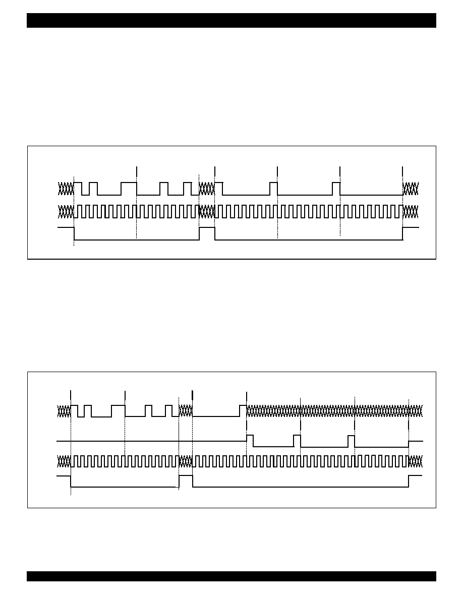
83
RSLIC (IDT82V1671) & CODEC (IDT82V1074) CHIPSET INDUSTRIAL TEMPERATURE RANGE
5.4
PROGRAMMING EXAMPLES
5.4.1
PROGRAMMING EXAMPLES FOR MPI MODE
5.4.1.1
Example of Programming the Local Registers via MPI
∑ Writing to LREG2 and LREG1 of Channel 1:
1010,0011
Channel Enable command
0001,0010
Data for GREG4 (Channel 1 is enabled for programming)
1000,0001
Local register write command (The address is '00001', means that data will be written to LREG2 and LREG1.)
0000,0001 Data
for
LREG2
0000,0000
Data for LREG1
∑ Reading LREG2 and LREG1 of Channel 1:
1010,0011
Channel Enable command
0001,0010
Data for GREG4 (Channel 1 is enabled for programming)
0000,0001
Local register read command (The address is '00001', means that LREG2 and LREG1 will be read.)
After the preceding commands are executed, data will be sent out as follows:
1000,0001
Identification code
0000,0001
Data read out from LREG2
0000,0000
Data read out from LREG1
Figure - 36 Waveform of Programming Example: Writing to Local Registers
Figure - 37 Waveform of Programming Example: Reading Local Registers
C I
C C L K
C S
C h a n n e l E n a b le
C o m m a n d
C h a n n e l E n a b le D a ta
L o ca l C o m m a n d
D a ta fo r L R E G 2
D a ta fo r L R E G 1
CI
CCLK
CS
Channel Enable
Com m and
Channel Enable Data
Local Com m and
Data read out from
LREG2
Data read out from
LREG1
CO
Identification Code
High 'Z'
High 'Z'

84
RSLIC (IDT82V1671) & CODEC (IDT82V1074) CHIPSET INDUSTRIAL TEMPERATURE RANGE
5.4.1.2
Example of Programming the Global Registers via MPI
Since the global registers are shared by all four channels, it is no need to specify the channel(s) before addressing global registers. Except for this,
programming global registers are the same as programming local registers. Refer to
"5.4.1.1 Example of Programming the Local Registers via MPI"
on page 83
for more information.
5.4.1.3
Example of Programming the Coefficient-RAM via MPI
∑ Writing to the Coe-RAM of Channel 1:
1010,0011
Channel Enable command
0001,0010
Data for GREG4 (Channel 1 is enabled for programming)
1110,0000
Coe-RAM write command (The address of '00000' is located in block 1, means that data will be written to block 1.)
byte 1
data for high byte of word 8 in block 1 (the highest two bits (b7b6) are ignored)
byte 2
data for low byte of word 8 in block 1
byte 3
data for high byte of word 7 in block 1 (the highest two bits (b7b6) are ignored)
byte 4
data for low byte of word 7 in block 1
byte 5
data for high byte of word 6 in block 1 (the highest two bits (b7b6) are ignored)
byte 6
data for low byte of word 6 in block 1
byte 7
data for high byte of word 5 in block 1 (the highest two bits (b7b6) are ignored)
byte 8
data for low byte of word 5 in block 1
byte 9
data for high byte of word 4 in block 1 (the highest two bits (b7b6) are ignored)
byte 10
data for low byte of word 4 in block 1
byte 11
data for high byte of word 3 in block 1 (the highest two bits (b7b6) are ignored)
byte 12
data for low byte of word 3 in block 1
byte 13
data for high byte of word 2 in block 1 (the highest two bits (b7b6) are ignored)
byte 14
data for low byte of word 2 in block 1
byte 15
data for high byte of word 1 in block 1 (the highest two bits (b7b6) are ignored)
byte 16
data for low byte of word 1 in block 1
∑ Reading from the Coe-RAM of Channel 1:
1010,0011
Channel Enable command
0001,0010
Data for GREG4 (Channel 1 is enabled for programming)
0110,0000
Coe-RAM read command (The address of '00000' is located in block 1, means that block 1 will be read.)
After the preceding commands are executed, data will be sent out as follows:
1000,0001
Identification code
byte 1
data read out from high byte of word 8 in block 1 (the highest two bits (b7b6) are meaningless)
byte 2
data read out from low byte of word 8 in block 1
byte 3
data read out from high byte of word 7 in block 1 (the highest two bits (b7b6) are meaningless)
byte 4
data read out from low byte of word 7 in block 1
byte 5
data read out from high byte of word 6 in block 1 (the highest two bits (b7b6) are meaningless)
byte 6
data read out from low byte of word 6 in block 1
byte 7
data read out from high byte of word 5 in block 1 (the highest two bits (b7b6) are meaningless)
byte 8
data read out from low byte of word 5 in block 1
byte 9
data read out from high byte of word 4 in block 1 (the highest two bits (b7b6) are meaningless)
byte 10
data read out from low byte of word 4 in block 1
byte 11
data read out from high byte of word 3 in block 1 (the highest two bits (b7b6) are meaningless)
byte 12
data read out from low byte of word 3 in block 1
byte 13
data read out from high byte of word 2 in block 1 (the highest two bits (b7b6) are meaningless)
byte 14
data read out from low byte of word 2 in block 1
byte 15
data read out from high byte of word 1 in block 1 (the highest two bits (b7b6) are meaningless)
byte 16
data read out from low byte of word 1 in block 1
5.4.1.4
Example of Programming the FSK-RAM via MPI
∑ Writing to the FSK-RAM:
1100,0001
FSK-RAM write command (The address is '00001', means that data will be written to word 2 and word 1.)
byte 1
data for high byte of word 2
byte 2
data for low byte of word 2
byte 3
data for high byte of word 1
byte 4
data for low byte of word 1

85
RSLIC (IDT82V1671) & CODEC (IDT82V1074) CHIPSET INDUSTRIAL TEMPERATURE RANGE
∑ Reading from the FSK-RAM:
0100,0001
FSK-RAM read command (The address is '00001', means that word 2 and word 1 will be read.)
After this command is executed, data will be sent out as follows:
1000,0001
Identification code
byte 1
data read out from high byte of word 2
byte 2
data read out from low byte of word 2
byte 3
data read out from high byte of word 1
byte 4
data read out from low byte of word 1
5.4.2
PROGRAMMING EXAMPLES FOR GCI MODE
5.4.2.1
Example of Programming the Local Registers via GCI
∑ Writing to LREG2 and LREG1 of Channel 1:
1000,0001
Program start command (provided channel A is the destination)
1000,0001
Local register write command (The address is '00001', means that data will be written to LREG2 and LREG1.)
0000,0001
data for LREG2
0000,0000
data for LREG1
∑ Reading from LREG2 and LREG1 of Channel 1:
1000,0001
Program start command (provided channel A is the source)
0000,0001
Local register read command (The address is '00001', means that LREG2 and LREG1 will be read.)
After the preceding commands are executed, data will be read out as follows:
1000,0001
Program start byte
0000,0001
data read out from LREG2
0000,0000
data read out from LREG1
5.4.2.2
Example of Programming the Global Registers via GCI
In GCI mode, the global registers are addressed in the similar manner as the local registers except the A/B bit in the Program Start byte is
neglected. See the descriptions above for details.
5.4.2.3
Example of Programming the Coefficient-RAM via GCI
∑ Writing to the Coe-RAM of Channel 1:
1000,0001
Program Start command (provided channel A is the destination)
1110,0000
Coe-RAM write command (The address is '00001', means that data will be written to block 1.)
byte 1
data for high byte of word 8 in block 1 (the highest two bits (b7b6) are ignored)
byte 2
data for low byte of word 8 in block 1
byte 3
data for high byte of word 7 in block 1 (the highest two bits (b7b6) are ignored)
byte 4
data for low byte of word 7 in block 1
byte 5
data for high byte of word 6 in block 1 (the highest two bits (b7b6) are ignored)
byte 6
data for low byte of word 6 in block 1
byte 7
data for high byte of word 5 in block 1 (the highest two bits (b7b6) are ignored)
byte 8
data for low byte of word 5 in block 1
byte 9
data for high byte of word 4 in block 1 (the highest two bits (b7b6) are ignored)
byte 10
data for low byte of word 4 in block 1
byte 11
data for high byte of word 3 in block 1 (the highest two bits (b7b6) are ignored)
byte 12
data for low byte of word 3 in block 1
byte 13
data for high byte of word 2 in block 1 (the highest two bits (b7b6) are ignored)
byte 14
data for low byte of word 2 in block 1
byte 15
data for high byte of word 1 in block 1 (the highest two bits (b7b6) are ignored)
byte 16
data for low byte of word 1 in block 1
∑ Reading from the Coe-RAM of Channel 1:
1000,0001
Program Start command (provided channel A is the source)
0110,0000
Coe-RAM read command (The address is '00000', means that block 1 will be read.)
After these commands are executed, data will be sent out as follows:
1000,0001
Program start byte
byte 1
data read out from high byte of word 8 in block 1 (the highest two bits (b7b6) are meaningless)

86
RSLIC (IDT82V1671) & CODEC (IDT82V1074) CHIPSET INDUSTRIAL TEMPERATURE RANGE
byte 2
data read out from low byte of word 8 in block 1
byte 3
data read out from high byte of word 7 in block 1 (the highest two bits (b7b6) are meaningless)
byte 4
data read out from low byte of word 7 in block 1
byte 5
data read out from high byte of word 6 in block 1 (the highest two bits (b7b6) are meaningless)
byte 6
data read out from low byte of word 6 in block 1
byte 7
data read out from high byte of word 5 in block 1 (the highest two bits (b7b6) are meaningless)
byte 8
data read out from low byte of word 5 in block 1
byte 9
data read out from high byte of word 4 in block 1 (the highest two bits (b7b6) are meaningless)
byte 10
data read out from low byte of word 4 in block 1
byte 11
data read out from high byte of word 3 in block 1 (the highest two bits (b7b6) are meaningless)
byte 12
data read out from low byte of word 3 in block 1
byte 13
data read out from high byte of word 2 in block 1 (the highest two bits (b7b6) are meaningless)
byte 14
data read out from low byte of word 2 in block 1
byte 15
data read out from high byte of word 1 in block 1 (the highest two bits (b7b6) are meaningless)
byte 16
data read out from low byte of word 1 in block 1
5.4.2.4
Example of Programming the FSK-RAM via GCI
∑ Writing to the FSK-RAM:
100X,0001
Program Start command
1100,0001
FSK-RAM write command (The address is '00001', means that data will be written to word 2 and word 1.)
byte 1
data for high byte of word 2
byte 2
data for low byte of word 2
byte 3
data for high byte of word 1
byte 4
data for low byte of word 1
∑ Reading from the FSK-RAM:
100X,0001
Program Start command
0100,0001
FSK-RAM read command (The address is '00001', means that word 2 and word 1 will be read.)
After the preceding commands are executed, data will be sent out as follows:
100X,0001
Program Start byte
byte 1
data read out from high byte of word 2
byte 2
data read out from low byte of word 2
byte 3
data read out from high byte of word 1
byte 4
data read out from low byte of word 1

87
RSLIC (IDT82V1671) & CODEC (IDT82V1074) CHIPSET INDUSTRIAL TEMPERATURE RANGE
6
OPERATIONAL DESCRIPTION
6.1
OPERATING MODES
In many applications, the system power consumption is an important
parameter. For large and remotely fed systems, this parameter is more
critical and must be limited to a given value to meet cooling
requirements and save power.
Generally, the system power dissipation is determined mainly by the
high-voltage part. The most effective power-saving method is to limit
SLIC functionality and reduce supply voltage in line according to
different requirements. The RSLIC-CODEC chipset achieves this goal
by providing different operating modes according to different loop states
or testing requirements. See the following descriptions for details.
6.1.1
RSLIC CONTROL SIGNALING
The CODEC provides three common mode selection pins M1 to M3
and four individual chip selection pins CS1 to CS4 for the four RSLICs to
control their operating modes. See
Figure - 38
for details.
The CS1 to CS4 pins of the CODEC are ternary logic pins as
illustrated in the following:
CSn = 0:
The CODEC will send mode control data to the RSLICn
through the M1 to M3 pins.
CSn = 1:
The CODEC will receive the temperature information of
the RSLICn through the M3 pin.
CSn = 1.5 V:The CODEC will not send or receive data to/from the
RSLICn through the M1 to M3 pins.
Note that the M3 pin of the CODEC is bidirectional. Its direction is
determined by the active CSn as described above.
Figure - 39
shows
the RSLIC control timing diagram.
Figure - 38 RSLIC Mode Control Signaling
M1~M3
CS1
CS2
CS3
M1~M3
CS
CS
RSLIC 1
#
CODEC
M1~M3
CS
RSLIC 2
#
M1~M3
CS
RSLIC 3
#
M1~M3
CS
RSLIC 4
#
CS4

88
RSLIC (IDT82V1671) & CODEC (IDT82V1074) CHIPSET INDUSTRIAL TEMPERATURE RANGE
Figure - 39 RSLIC Control Timing Diagram
M3 I/O Control
M3
M2
M1
CS4
CS3
CS2
CS1
FS
125 µs
31.25 µs
7.8125 µs
output
output
output
output
input
input
input
input
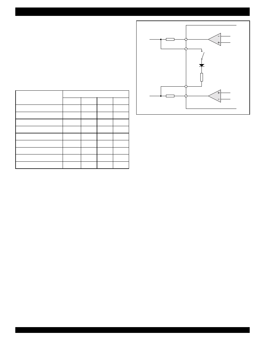
89
RSLIC (IDT82V1671) & CODEC (IDT82V1074) CHIPSET INDUSTRIAL TEMPERATURE RANGE
6.1.2
RSLIC OPERATING MODES
The RSLICs can be operated in nine different modes as shown in
Table - 26
. The operating mode is configured by the SM[2:0] bits in
LREG6 (MPI mode) or in the downstream C/I channel (GCI mode).
The SCAN_EN bit in LREG6 (MPI mode) or downstream C/I channel
(GCI mode) determines whether the corresponding RSLIC will be
accessed. If this bit is set to 1, the RSLIC will receive data from the
CODEC when the corresponding CSn pin is logic low and transmit data
to the CODEC when the corresponding CSn pin is logic high (as
illustrated in
Figure - 39
). If this bit is set to 0, the corresponding CSn pin
will be set to 1.5 V and the RSLIC will not be accessed.
∑ Normal Active
In this mode, a regular call can be performed. Voice can be
transferred via the telephone line. Besides providing low-impedance
voltage (VBL) feeding to the line, the RSLIC senses, scales and
separates transversal and longitudinal line currents.
∑ External Ring
The RSLIC receives an external ringing signal provided at pins RSP
and RSN and feeds it to the telephone line. The RSLIC also provides a
ring trip signal for the CODEC via the RT pin.
∑ Internal Ring
The CODEC generates a balanced ringing signal and outputs it to
the RSLIC through the DCP and DCN pins. The RSLIC amplifies this
ringing signal and feeds it to the telephone line.
∑ Ring Open
In ring open mode, the ring power amplifier is switched off and the
ring terminal presents a high impedance to the line. This mode is used to
measure the leakage current Tip/GND.
∑ Tip Open
In tip open mode, the tip power amplifier is switched off and the tip
terminal presents a high impedance to the line. This mode is used for
ground-key detection and the leakage current Ring/GND measurement.
∑ Internal Test
This mode can be used to test the RSLIC-CODEC chipset without
external circuits.
When the RSLIC is set to internal test mode, it works in a similar way
as normal active mode. The only difference is that a built-in resistor will
be connected between the TIP and RING pins to form a loop for testing.
See
Figure - 40
for details.
∑ Low Power Standby
In this mode, all functions except off-hook detection are switched off
to reduce power consumption. Two 2.5 k
resistors are connected from
TIP to BGND and from RING to VBAT respectively. A simple sense
circuit monitors the DC current flowing through these resistors. By
calculating the transversal DC current and feeding it to the CODEC, off-
hook can be detected. Once the subscriber goes off-hook, the whole
chipset should be activated and put into active mode.
∑ Power Down
In this mode, all functions are disabled, including the off-hook
detection. The tip and ring power amplifiers are both switched off so that
the power consumption is minimal.
∑ Overtemp Check
In this mode, the RSLIC will report the temperature state of itself to
the CODEC through the M3 pin. This temperature state will be indicated
by the OTMP bit in LREG21. If the temperature exceeds the limit
(150
o
C), the RSLIC will be automatically shut down. Every time the
OTMP bit changes from 0 to 1, representing the temperature of the
RSLIC becoming overloaded, an interrupt will be generated if the OTMP
bit is not masked by the OTMP_M bit in LREG18.
6.1.3
CODEC OPERATING MODES
The CODEC can work in five modes: Power Down, Standby, Active,
Ramp and Ring. These modes are enabled by setting the P_DOWN,
STANDBY, ACTIVE and RAMP bits in LREG6 and RING bit in LREG7
respectively.
∑ Power Down
This mode is applicable for the line (channel) that is not in use. In this
mode, all functions of the CODEC are switched off so that the power
dissipation can be minimized. Both AC and DC loops are inactive, no
current is fed to the line and the hook switch can not be detected.
Each channel of the CODEC can be powered down individually by
setting the P_DOWN bit in corresponding LREG6. If four channels are
powered down, the clock cycles fed to the MCLK and BCLK pins should
be shut off to achieve the lowest power consumption.
The CODEC can be changed from Power Down mode to any other
modes by properly setting LREG6 and LREG7.
Table - 26 RSLIC Operating Mode
RSLIC Operating Mode
RSLIC Mode Control Pins
CS
M3
M2
M1
Normal Active
0
0
0
0
External Ring
0
0
0
1
Internal Ring
0
0
1
0
Ring Open
0
0
1
1
Tip Open
0
1
0
0
Internal Test
0
1
0
1
Low Power Standby
0
1
1
0
Power Down
0
1
1
1
Overtemp Check (read)
1
X
1
1
Figure - 40 RSLIC Internal Test Circuit
R
S
TIS
TIP
RING
RIS
R
S
RSLIC
2 k

90
RSLIC (IDT82V1671) & CODEC (IDT82V1074) CHIPSET INDUSTRIAL TEMPERATURE RANGE
∑ Standby
The standby mode is applicable for system state of subscriber being
on-hook. In this mode, only the AC loop is active, all functions except for
the off-hook detection are switched off. The sensed voltage from the
RSLIC is fed to an analog comparator in the CODEC via VTAC pin. The
loop state can be determined by comparing the sensed voltage with a
fixed off-hook threshold. If off-hook state is detected, the overall circuits
should be activated and switched to the active mode.
∑ Active
The active mode corresponds to the system state of off-hook. In this
mode, both AC and DC loops are active. The RSLIC provides low-
impedance voltage (VBL) fed to the line. The RSLIC senses the
transversal and longitudinal line currents and separates the transversal
current to AC and DC parts. The CODEC scales the currents and
converts the AC part of the transversal current to voice data. On the
other hand, the CODEC expands the voice data from the PCM bus and
converts them to an analog signal. The DC voltage fed to the line can be
automatically achieved by the chipset according to certain loop lengths,
power optimized solution.
∑ Ring
This mode corresponds to the system state of ringing. The chipset
provides both internal ringing and external ringing modes to be selected.
Refer to
Table - 26
for details.
If internal ringing mode is selected, an internal balanced ringing
signal of up to 70 Vp (with high voltage battery (VBH) of 70 V) can be
generated without any external components. In applications that high
ringing voltage is not needed, a DC offset can be added to support the
DC ring trip detection, which is more reliable than AC ring trip detection.
If an external ring generator and ring relays are used, the RSLIC can
be switched to power down mode. An individual operation amplifier in
the RSLIC is supplied for ring trip detection.
∑ Ramp
If ramp mode is selected (LREG6: RAMP = 1), the integrated ramp
generator in the CODEC is active and able to generate a ramp signal to
help measuring the capacitance. The ramp generator is fully
programmable. By programming the ramp slope, ramp start voltage and
end voltage, a desired ramp can be generated by the CODEC and
output to the line via the RLSIC. With this ramp signal as the source, the
line capacitance can be measured via the DC level meter. See
"3.9.6.5
Capacitance Measurement" on page 47
for detailed information.
6.2
PLL POWER DOWN
The PLL_PD bit in GREG1 is used to power down the PLL block of
the CODEC to reduce the power consumption. If the PLL_PD bit is set to
1, the PLL block is turned off and the DSP operation is disabled. As
described above, each of the channels can be individually powered
down by setting the corresponding P_DOWN bit in LREG6 to 1. When
all four channels and the PLL block are powered down, the lowest power
consumption can be achieved.
6.3
PROGRAMMABLE I/OS OF THE CODEC
The CODEC provides four programmable IO pins per channel as
shown in the following:
IO1:
IO pin with relay-driving capability
IO2:
IO pin with relay-driving capability
IO3:
IO pin with analog input capability
IO4:
IO pin with analog input capability
The four IO pins IO4 to IO1 can be independently configured as input
or output by the corresponding control bits IO_C[3] to IO_C[0] in
LREG20.
If the IO pins are configured as inputs, the status of the IO pins will be
indicated by the IO[3:0] bits in LREG20. If the IO pins are configured as
outputs, the data written in the IO[3:0] bits in LREG20 will be sent out
through the IO pins.
If the IO1 and IO2 pins are configured as outputs, they are capable of
driving external relays. Based on this, the IO1 pin automatically acts as
an output to control the external ring relay when external ringing mode is
selected. Refer to
"3.4.2 External Ringing Mode" on page 24
for details.
If the IO3 and IO4 pins are configured as inputs, they are capable of
receiving analog inputs. With this capability external voltages can be fed
to the DC level meter via the IO3 and/or IO4 pins to be measured. Refer
to
"3.9.6.6 Voltage Measurement" on page 48
for details.
The input signals from the four IOs will be filtered by a programmable
debounce filter (see
Figure - 41
). The output of the debounce filter
remains in its present state unless the input remains in the opposite
state for the entire period of time programmed by the DB_IO[3:0] bits in
LREG11. The debounce period is programmable from 0 ms to 30 ms in
steps of 2 ms, corresponding to the minimal debounce time of 2.5 ms to
32.5 ms (a delay time of about 2.5 ms added). The default value of
DB_IO[3:0] is `0000'.
Figure - 41 IO Debounce Filter
DB_IO[3:0]
Debounce Period
(0
- 30ms)
8 bit Debounce
Counter
Debounced IO
IO
FS
Q
D
RST
Q
Q
Q
D
D
D
Q
D
En

91
RSLIC (IDT82V1671) & CODEC (IDT82V1074) CHIPSET INDUSTRIAL TEMPERATURE RANGE
The debounced IO data are stored in the IO[3:0] bits in LREG20. The
four bits IO[3] to IO[0] have their respective mask bits - IO_M[3] to
IO_M[0] in LREG19. Each change of the IO[n] bit will generate an
interrupt if its mask bit IO_M[n] is set to 0 (n = 0 to 3).
6.4
INTERRUPT HANDLING
The RSLIC-CODEC chipset is capable of generating interrupts for
the following event:
∑ Off-hook/on-hook detected
∑ ground-key detected
∑ ground-key polarity changed
∑ Ring trip detected
∑ IO status changed
∑ Over temperature detected
∑ Level metering finished
∑ Special tone detected
∑ Ramp generation finished
The interrupt status register GREG26 contains the results of hook/
ring trip detection and ground-key detection for four channels (two bits
per channel). Other interrupt status of each channel is contained by the
respective interrupt status registers LREG20 and LREG21 (each
interrupt function has one bit). These bits are set when an interrupt is
pending for the associated source. Two interrupt mask registers
(LREG18 and LREG19) per channel contain one mask bit for each of
the above interrupt functions except special tone detected and level
metering completed. If a mask bit is set to high, the corresponding
interrupt will be masked. Refer to
Table - 27
for detailed information.
In MPI mode, the interrupt output pin INT/INT will be set to active
level if any interrupt is generated. In GCI mode, if any interrupt is
generated in a channel, the corresponding INT_CHA or INT_CHB bit in
upstream C/I channel will be set to active level. The valid polarity of the
INT/INT pin and the INT_CHA, INT_CHB bits is determined by the
INT_POL bit in register GREG24 as shown below:
INT_POL = 0: active low;
INT_POL = 1: active high.
In both MPI and GCI mode, the pending interrupts can be cleared by
a read operation on the corresponding interrupt register. For example,
reading GREG26 clears the interrupts generated by hook/ring trip
detection and ground-key detection. Additionally, the CODEC provides a
dedicated command to clear all the interrupts at one time. That is, by
applying a write operation to GREG26, all the global and local interrupt
status registers will be cleared.
A hardware or power-on reset of the CODEC clears all interrupt
status registers and resets the INT/INT pin to inactive (MPI mode) or
resets the INT_CHA and INT_CHB bits in the GCI C/I channel (GCI
mode). A software reset applied to one channel clears all local interrupt
status registers of that channel but does not effect those of the other
channels and the global interrupt status register.
6.5
SIGNAL PATH AND TEST LOOPBACKS
Figure - 42
on the following page shows the main AC and DC signal
paths and the integrated analog and digital loopbacks inside the
CODEC. Refer to the register descriptions on GREG6 and LREG3 for
details.
Table - 27 Interrupt Source and Interrupt Mask
Interrupt Source
Status bits
Interrupt Generating Conditions
Mask Bit
Hook Status
HK[n] bit in GREG26 (n = 0 to 3)
Each change of the HK[n] bit
HK_M bit in LREG18
Ground-key Status
GK[n] bit in GREG26 (n = 0 to 3)
Each change of the GK[n] bit
GK_M bit in LREG18
Ring Trip Status
HK[n] bit in GREG26 (n = 0 to 3)
Each change of the HK[n] bit
HK_M bit in LREG18
RSLIC IO Status
IO[n] bit in LREG20 (n = 0 to 3)
Each change of the IO[n] bit when the corresponding IO
pin is configured as an input
IO_M[n] bit in LREG19
Ground-key Polarity
GK_POL bit in LREG21
Each change of the GK_POL bit
GKP_M bit in LREG18
Over Temperature Status
OTMP bit in LREG21
A change of the OTMP bit from 0 to 1
OTMP_M bit in LREG18
Ramp Generation
RAMP_OK bit in LREG21
A change of the RAMP_OK bit from 0 to 1
RAMP_M bit in LREG18
UTD Result
UTD_OK bit in LREG21
A change of the UTD_OK bit from 0 to 1
None
Level Meter Sequence
LM_OK bit in LREG21
A change of the LM_OK bit from 0 to 1
None

92
RSLIC (IDT82V1671) & CODEC (IDT82V1074) CHIPSET INDUSTRIAL TEMPERATURE RANGE
Figure - 42 AC/DC Signal Path and Test Loopbacks
An
t
i
-
A
l
i
a
s
Fil
t
e
r
(
A
A
F
)
Sigma
-
Delt
a
Mo
d
u
l
a
t
o
r
(S
D
M
)
Ga
i
n
Tr
a
n
s
m
i
t
(G
T
X
)
Lo
w-Pa
s
s
Fi
l
t
e
r
Tr
a
n
s
m
i
t
2n
d
De
c
i
m
a
t
i
on
Fil
t
e
r
Fr
eq
ue
ncy R
e
spon
se
Co
rre
ct
i
o
n T
r
an
s
m
i
t
(F
R
X
)
Hi
g
h
-
P
as
s
Fi
l
t
e
r
T
r
an
sm
i
t
(H
P
F
)
2nd
In
te
rp
o
l
a
t
io
n
F
ilt
e
r
Ga
i
n
Re
c
e
i
v
e
(G
R
X
)
3r
d
In
te
rp
o
l
a
t
io
n
Fi
l
t
e
r
I
m
pe
da
n
c
e
M
a
t
c
hi
ng
Fi
lt
er
(
I
MF)
Tr
an
shb
r
i
d
B
a
la
n
c
e
Fi
lt
e
r
(E
C
F
)
1s
t
I
n
t
e
r
pol
at
i
o
n
Fi
l
t
er
1s
t
De
c
i
m
a
t
i
on
Fi
l
t
er
PCM
E
n
co
der
PCM
Dec
o
de
r
F
r
equ
en
cy R
e
sp
ons
e
Cor
r
e
c
t
i
o
n
Re
c
e
i
v
e
(F
R
R
)
Lo
w
-
Pa
ss
Fil
t
e
r
Re
c
e
i
v
e
Si
g
m
a-
De
l
t
a
Demo
du
l
a
t
o
r
(D
-S
D
M
)
Smoo
t
h
i
n
g
Fi
lt
er
&
SC
F
G
a
in
fo
r
I
m
pe
dan
ce
S
c
al
i
ng (
G
I
S
)
A
n
a
l
o
g
G
a
in
fo
r
I
m
pe
dan
ce
Sc
al
i
n
g (A
GI
S)
UT
D
TG1
TG2
CUT
OFF
Ti
me
Slot
A
ssi
gn
men
t
Ti
m
e
S
l
ot
A
ssi
gn
men
t
DLB
_
2
M
ALB
_
2
M
D
L
B
_
64K
AL
B_
64
K
DL
B_
8K
AL
B_
8K
SE
L
UTD_
EN
UT
DSRC
DL
B_
PCM
A
L
B_
PC
M
UT
D_
O
K
DL
B_
DI
AL
B_D
I
GKD
C
o
m
p
ar
at
o
r
MUX
ADC
1.
0
24M
Hz
DC1
Lo
op
F
ilte
r(D
C
)
POF
I
L
DAC
IN
T
E
R
P
Ri
n
g
G
e
ner
a
t
or
Loo
p Fe
ed
i
n
g
Al
go
r
i
t
h
m
Ho
ok
Detec
t
i
o
n
DC
OF
FSE
T
R
i
ng T
r
i
p
De
t
e
c
t
or
Ra
m
p
Ge
ne
r
a
t
o
r
RAMP
_OK
H
ook
In
d
i
c
a
tio
n
Re
v
P
ol
DC2
Le
vel
M
e
t
e
r
SE
L
DC
_
S
R
C
LM
_
S
RC
DCN/
DC
P
VC
M
VD
D
IO
4
-
IO
3
IO
4
IO
3
VTDC
VREF
VL
R
i
ngD
C
RTI
N
"0
"
"1"
"0
"
RT
P
OF
FSE
T
Ba
nd
pass
/
N
o
t
c
h Fi
l
t
er
LM
_F
I
L
T
VL
AL
B_
1MDC
SE
L
ACP/
AC
N
VT
AC
DX
1/
DX
2
DR1
/
DR2
An
al
og
@2
M
H
z
@
16k
H
z
@6
4k
H
z
@8
kHz
TS
PCM H
i
gh
wa
y
"1
"
O
f
f
-
h
ook
C
o
m
p
ar
at
o
r
VREF
LM
OUT
GREG6
:
LR
E
G
3:
MSB
LS
B
MSB
LS
B
T
hese
l
o
op
back
s
ar
e
c
ont
r
o
l
l
ed
b
y
r
e
g
i
s
t
e
r
s G
R
EG
6
and
LR
E
G
3 as sh
ow
n
b
e
l
o
w
.
Ea
ch o
f
t
h
e
l
o
opb
ack
s
i
s
c
l
o
s
ed
by se
t
t
i
n
g
t
h
e cor
r
e
s
po
nd
i
n
g bi
t
t
o
1 an
d op
ene
d by s
e
t
t
i
n
g
t
he co
r
r
e
sp
on
di
ng b
i
t
t
o
0.
N
o
t
e
t
h
at
t
h
e f
o
u
r
l
o
o
p
b
a
cks
A
L
B_
DI
,
D
L
B
_
D
I
,
AL
B
_
P
C
M
and
D
L
B
_
P
CM
a
r
e av
ai
l
a
bl
e f
o
r
M
P
I
m
o
d
e
on
l
y
.
Re
s
e
r
v
e
d
AL
B
_64
K
AL
B_
8K
ALB
_
D
I
Res
e
r
v
ed
DL
B
_64
K
DLB
_
8
K
DLB
_
DI
Re
s
e
r
v
e
d
DL
B_
2M
DL
B_
PCM
Res
e
r
v
ed
ALB
_
1
M
DC
AL
B_
2M
AL
B_
PC
M
CU
TOFF

93
RSLIC (IDT82V1671) & CODEC (IDT82V1074) CHIPSET INDUSTRIAL TEMPERATURE RANGE
6.6
RSLIC POWER ON SEQUENCE
It is recommended to power on the RSLIC following the sequence
below:
1. Apply Ground to the AGND and BGND pins;
2. Apply +3.3 V power supply to the VDD pin;
3. Apply battery voltage
(
-70 V VBH -52 V)
to the VBH pin;
4. Apply battery voltage
(
-52 V VBL -20 V)
to the VBL pin;
But if the recommended application circuit (
Figure - 49 on page 104
or
Figure - 50 on page 105
) is used, the above mentioned RSLIC power
on sequence is not necessary.
6.7
CODEC POWER ON SEQUENCE
To power on the CODEC, the operating sequence should be as
follows:
1. Apply Ground to all ground pins;
2. Apply VDD voltage to all power supply pins;
3. Select master clock frequency (via GREG4);
4. Program filter coefficients and other parameters as required.
6.8
DEFAULT STATE AFTER RESET
6.8.1
POWER-ON RESET AND HARDWARE RESET
The CODEC can be reset by a power-on reset or a hardware reset. A
hardware reset of the CODEC can be accomplished by setting the signal
to the RESET pin to low level for at least 50 µs or setting the HW_RST
bit in GREG5 to 1. After a power-on reset or a hardware reset, the
default register settings are used. The CODEC will then enter the default
state as described below:
1. All four channels are powered down;
2. All loopbacks and cutoff are disabled;
3. The DX1/DU pin is selected for all channels to transmit PCM
data. The DR1/DD pin is selected for all channels to receive PCM
data.
4. The master clock (MCLK) frequency is 2.048 MHz;
5. In MPI mode, Time Slot 0 to Time Slot 3 are selected for Channel
1 to Channel 4 to transmit and receive data. The PCM data rate is
the same as the Bit Clock (BCLK) frequency. The PCM data is
transmitted on the rising edges of BCLK and received on the
falling edges.
In GCI mode, time slot assignment is determined by the logic
levels of the CCLK/S0 and CI/S1 pins. The data rate is always
2.048 MHz, no matter 2.048 MHz or 4.096 MHz is applied to the
DCL pin. The GCI data is transferred via the DU/DD pin on rising
edges of DCL.
6. A-law is selected;
7. Default register settings are selected;
8. All IO pins are configured as inputs;
9. All maskable interrupts are masked by corresponding mask bits;
10.All function blocks including level meter, UTD unit, FSK generator,
tone generators etc., are disabled.
6.8.2
SOFTWARE RESET
Each channel of the CODEC can be individually reset by a software
reset command. The RCH_SEL[3:0] bits in GREG5 determine whether
Channel 4 to Channel 1 will be software reset or not. Setting the
SW_RST bit and any desired bit of RCH_SEL[3:0] to 1 will reset the
corresponding channel. Once a software reset is performed, the device
will enter the following state:
1. The reset channel(s) are powered down;
2. All test loopbacks and cutoff on the reset channel(s) are disabled;
3. The DX1/DU and DR1/DD pins are selected for the reset
channel(s) to transmit and receive PCM data.
4. In MPI mode, Time Slot 0 to Time Slot 3 are selected for Channel
1 to Channel 4 to transmit and receive the PCM data. The PCM
data rate is the same as the Bit Clock (BCLK) frequency. The
PCM data is transmitted on the rising edges of BCLK and
received on the falling edges.
In GCI mode, time slot assignment is determined by the logic
levels of the CCLK/S0 and CI/S1 pins. The data rate is always
2.048 MHz, no matter 2.048 MHz or 4.096 MHz is applied to the
DCL pin. The GCI data is transferred via DU/DD pin on rising
edges of DCL.
5. All default coefficients and register setting except the highpass
filter (the HPF bit in LREG5 is set to 1) are selected for the reset
channel(s).
6. All IO pins of the reset channel(s) are configured as inputs;
7. All maskable interrupts of the reset channel(s) are masked by
corresponding mask bits.

94
RSLIC (IDT82V1671) & CODEC (IDT82V1074) CHIPSET INDUSTRIAL TEMPERATURE RANGE
7
ELECTRICAL CHARACTERISTICS
7.1
RSLIC ELECTRICAL CHARACTERISTICS
7.1.1
RSLIC ABSOLUTE MAXIMUM RATINGS
∑
Note: Stresses greater than those listed under ABSOLUTE MAXIMUM RATINGS may cause permanent damage to the device. This is a stress rating only and functional operation of the
device at these or any other conditions above those indicated in the operational sections of this specification is not implied. Exposure to absolute maximum rating conditions for extended
periods may affect reliability.
7.1.2
RSLIC RECOMMENDED OPERATING CONDITIONS
∑
7.1.3
RSLIC THERMAL INFORMATION
∑
7.1.4
RSLIC POWER CONSUMPTION
∑
Ratings
Min.
Max.
Unit
Power supply voltage VDD
-0.5
+5
V
VDD-VBH
75
V
Tip/Ring negative pulse
VBH
- 0.7
V
Tip/Ring positive pulse
VDD
+ 0.7
V
ESD voltage (Human body model)
1
kV
Parameter
Min.
Max.
Unit
Operating temperature
-40
+85
∞C
Power supply voltage VDD
+3.135
+3.465
V
Low battery power supply VBL
-52
-20
V
High battery power supply VBH
-70
-52
V
Parameter
Min.
Max.
Unit
Thermal resistance
70
∞C/W
Maximum junction temperature (plastic)
150
∞C
Description
Min.
Typ.
Max.
Units
Test Conditions
RSLIC power consumption in power down mode
90
100
mW
VDD = +3.3 V, VBH =
-70 V, VBL = -48 V;
without load.between the Tip pin and the
Ring pin.
RSLIC power consumption in standby mode
160
180
mW
RSLIC power consumption in normal active mode
400
450
mW

95
RSLIC (IDT82V1671) & CODEC (IDT82V1074) CHIPSET INDUSTRIAL TEMPERATURE RANGE
7.2
CODEC ELECTRICAL CHARACTERISTICS
7.2.1
CODEC ABSOLUTE MAXIMUM RATINGS
∑
Note: Stresses greater than those listed under ABSOLUTE MAXIMUM RATINGS may cause permanent damage to the device. This is a stress rating only and functional operation of the
device at these or any other conditions above those indicated in the operational sections of this specification is not implied. Exposure to absolute maximum rating conditions for extended
periods may affect reliability.
7.2.2
CODEC RECOMMENDED OPERATING CONDITIONS
∑
7.2.3
CODEC DIGITAL INTERFACE
∑
7.2.4
CODEC POWER DISSIPATION
∑
Ratings
Min.
Max.
Unit
Supply pins referred to the corresponding ground pin
-0.3
4.6
V
Ground pins referred to any other ground pin
-0.3
+0.3
V
Supply pins referred to any other supply pin
-0.3
+0.3
V
Analog input and output pins
-0.3
3.6
V
Digital input and output pins
-0.3
5.5
V
DC input and output current at any input or output pin (free from latch-up)
100
mA
Storage temperature
-65
125
∞C
Ambient temperature under bias
-40
85
∞C
Power dissipation
1
W
ESD voltage (Human body model)
2
kV
Description
Min.
Typ.
Max.
Units
Test Conditions
Supply pins referred to the corresponding ground pin
+3.135
+3.3
+3.465
V
Analog input pins referred to the ground pin
0
+3.3
V
Ambient temperature
-40
+85
∞C
Parameter
Description
Min.
Typ.
Max.
Units
Test Conditions
V
IL
Input low voltage
0.8
V
All digital inputs
V
IH
Input high voltage
2.0
V
All digital inputs
V
OL
Output low voltage
0.8
V
I
L
= 4 mA
V
OH
Output high voltage
VDD
- 0.6
V
I
L
=
-4 mA
V
AOL
Output low voltage on relay driver pin
0.4
V
I
L
= 10 mA
V
AOH
Output high voltage on relay driver pin
VDD
- 0.6
V
I
L
=
-4 mA
I
I
Input current
-10
10
µA
All digital inputs
I
OZ
Output current in high-impedance digital pin
-10
10
µA
C
I
Input capacitance
5
pF
Parameter
Description
Min.
Typ.
Max.
Units
Test Conditions
VDD
Power supply voltage
3.3
V
I
DD1
Operating current
95
mA
I
DD0
Standby current
7
mA
96
RSLIC (IDT82V1671) & CODEC (IDT82V1074) CHIPSET INDUSTRIAL TEMPERATURE RANGE
7.3
CHIPSET TRANSMISSION CHARACTERISTICS
0 dBm0 of PCM bus is defined as 0.775 Vrms for 600
load. 0 dBm0 of analog input or output of the CODEC is relative to the 0 dBm0 of the PCM
bus output or input. Unless otherwise noted, the analog input is a 0 dBm0, 1020 Hz sine wave. The digital input is a PCM bit stream equivalent to that
obtained by passing a 0 dBm0, 1020 Hz sine wave through an ideal encoder. The output level is sin(x)/x-corrected. Typical values are tested at VDD
= 3.3 V and T
A
= 25∞C.
7.3.1
ABSOLUTE GAIN
∑
7.3.2
GAIN TRACKING
∑
7.3.3
FREQUENCY RESPONSE
∑
7.3.4
RETURN LOSS
∑
Parameter
Description
Min.
Typ.
Max.
Units
Test Conditions
G
XA
Transmit gain, absolute
-0.25
0.25
dB
Signal output of 0 dBm0, normal mode
G
RA
Receive gain, absolute
-0.25
0.25
dB
A-law or µ-law, PCM input of 0 dBm0, 1014 Hz
Parameter
Description
Min.
Typ.
Max.
Units
Test Conditions
G
TX
Transmit gain tracking
+3 dBm0 to -40 dBm0
-40 dBm0 to -50 dBm0
-50 dBm0 to -55 dBm0
-0.25
-0.5
-1.4
0.25
0.5
1.4
dB
Tested by sinusoidal method, A-law or µ-law,
f = 1014 Hz, reference level
-10 dBm0
G
TR
Receive gain tracking
+3 dBm0 to -40 dBm0
-40 dBm0 to -50 dBm0
-50 dBm0 to -55 dBm0
-0.25
-0.5
-1.4
0.25
0.5
1.4
dB
Tested by sinusoidal method, A-law or µ-law,
f = 1014 Hz, reference level
-10 dBm0
Parameter
Description
Min.
Typ.
Max.
Units
Test Conditions
G
XR
Transmit gain, relative to G
XA
f = 50 Hz
f = 60 Hz
f = 300 Hz to 3000 Hz
f = 3000 Hz to 3400 Hz
f = 3600 Hz
f
4600 Hz
-0.25
-0.40
-30
-30
0.25
0.25
-0.10
-35
dB
The highpass filter is enabled.
G
RR
Receive gain, relative to G
RA
f < 300 Hz
f = 300 Hz to 3000 Hz
f = 3000 Hz to 3400 Hz
f = 3600 Hz
f
4600 Hz
-0.25
-0.40
0.10
0.25
0.25
-0.20
-35
dB
Parameter
Description
Min.
Typ.
Max.
Units
Test Conditions
RL
Return loss (2-wire)
26
dB
300 - 3400 Hz
HB
Hybrid balance (4-wire)
26
dB
300 - 3400 Hz
L-4
Input longitudinal interface loss
52
55
dB
300 - 3400 Hz
L-T
Longitudinal conversion loss
52
55
dB
300 - 3400 Hz
97
RSLIC (IDT82V1671) & CODEC (IDT82V1074) CHIPSET INDUSTRIAL TEMPERATURE RANGE
7.3.5
GROUP DELAY
∑
7.3.6
DISTORTION
∑
7.3.7
NOISE
∑
Parameter
Description
Min.
Typ.
Max.
Units
Test Conditions
D
XR
Transmit delay, relative to 1800 Hz
f = 500 Hz to 600 Hz
f = 600 Hz to 1000 Hz
f = 1000 Hz to 2600 Hz
f = 2600 Hz to 2800 Hz
80
80
50
280
µs
D
RR
Receive delay, relative to 1800 Hz
f < 300 Hz
f = 300 Hz to 3400 Hz
f = 3600 Hz
f
4600 Hz
50
80
120
150
µs
DR
Round-trip delay
900
µs
Parameter
Description
Min.
Typ.
Max.
Units
Test Conditions
STD
X
Transmit signal to total distortion ratio
-45 dBm0
-40 dBm0
-30 dBm0
-20 dBm0
-10 dBm0
3 dBm0
25
29
34
36
36
36
dB
Output connection: L
X
= 0 dBr
f = 1014 Hz (C message weighted for µ-law,
psophometrically weighted for A-law)
STD
R
Receive signal to total distortion ratio
-45 dBm0
-40 dBm0
-30 dBm0
-20 dBm0
-10 dBm0
3 dBm0
25
29
34
36
36
36
dB
Input connection: L
R
= 0 dBr
f = 1014 Hz (C message weighted for µ-law,
psophometrically weighted for A-law)
Parameter
Description
Min.
Typ.
Max.
Units
Test Conditions
N
XC
Transmit noise, C message weighted for µ-law
18
dBrnC0
N
XP
Transmit noise, psophometrically weighted for A-law
-68
dBm0p
N
RC
Receive noise, C message weighted for µ-law
12
dBrnC0
N
RP
Receive noise, psophometrically weighted for A-law
-78
dBm0
PSR
X
Power supply rejection, transmit
f = 300 Hz to 3.4 kHz
f = 3.4 kHz to 20 kHz
30
25
dB
VDD = 3.3 VDC+100 mVrms
PSR
R
Power supply rejection, receive
f = 300 Hz to 3.4 kHz
f = 3.4 kHz to 20 kHz
30
25
dB
VDD = 3.3 VDC+100 mVrms, PCM code is
positive LSB one

98
RSLIC (IDT82V1671) & CODEC (IDT82V1074) CHIPSET INDUSTRIAL TEMPERATURE RANGE
7.3.8
INTERCHANNEL CROSSTALK
∑
Parameter
Description
Min.
Typ.
Max.
Units
Test Conditions
XT
X-R
Transmit to receive crosstalk
-85
-78
dB
300 Hz to 3400 Hz, 0 dBm0 signal into VTAC of
interfering channel. Idle PCM code into channel
under test
XT
R-X
Receive to transmit crosstalk
-85
-80
dB
300 Hz to 3400 Hz, 0 dBm0 PCM code into inter-
fering channel. VTAC = 0 Vrms for channel
under test
XT
X-X
Transmit to transmit crosstalk
-85
-78
dB
300 Hz to 3400 Hz, 0 dBm0 signal into VTAC of
interfering channel. VTAC = 0 Vrms for channel
under test
XT
R-R
Receive to receive crosstalk
-85
-80
dB
300 Hz to 3400 Hz, 0 dBm0 PCM code into inter-
fering channel. Idle PCM code into channel
under test
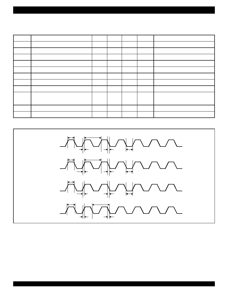
99
RSLIC (IDT82V1671) & CODEC (IDT82V1074) CHIPSET INDUSTRIAL TEMPERATURE RANGE
7.4
CODEC TIMING CHARACTERISTICS
7.4.1
CLOCK TIMING
∑
∑
Symbol
Description
Min.
Typ.
Max.
Units
Test Conditions
t1
CCLK period
122
100 k
ns
t2
CCLK pulse width
48
ns
t3
CCLK rise and fall time
25
ns
t4
BCLK period
122
ns
t5
BCLK pulse width
48
ns
t6
BCLK rise and fall time
15
ns
t7
MCLK pulse width
48
ns
t8
MCLK rise and fall time
15
ns
t9
DCL period
f = 2.048 kHz
f = 4.096 kHz
488
244
ns
t10
DCL rise and fall time
60
ns
t11
DCL pulse width
90
ns
∑
Figure - 43 Clock Timing
t3
t3
CCLK
t1
t2
t2
t6
t6
BCLK
t4
t5
t5
t8
t8
MCLK
t7
t7
t10
t10
DCL
t9
t11

100
RSLIC (IDT82V1671) & CODEC (IDT82V1074) CHIPSET INDUSTRIAL TEMPERATURE RANGE
7.4.2
MICROPROCESSOR INTERFACE TIMING
∑
∑
∑
Symbol
Description
Min.
Typ.
Max.
Units
Test Conditions
t12
CS setup time
15
ns
t13
CS pulse width
8
n t1
(n
2)
ns
t14
CS off time
250
ns
t15
Input data setup time
30
ns
t16
Input data hold time
30
ns
t17
SLIC output latch valid
1000
ns
t18
Output data turn on delay
50
ns
t19
Output data hold time
0
ns
t20
Output data turn off delay
50
ns
t21
output data valid
0
50
ns
∑
Figure - 44 MPI Input Timing
∑
Figure - 45 MPI Output Timing
t12
t15
t16
t14
t17
CCLK
CS
CI
RSLIC
Output
t13
t12
t18
t19
t14
CCLK
CS
CO
t13
t21
t20
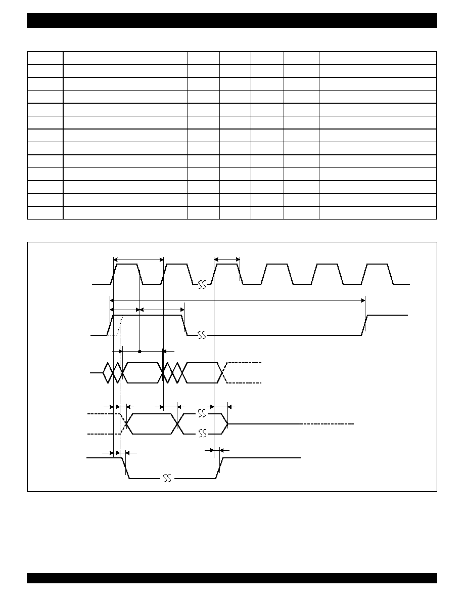
101
RSLIC (IDT82V1671) & CODEC (IDT82V1074) CHIPSET INDUSTRIAL TEMPERATURE RANGE
7.4.3
PCM INTERFACE TIMING
∑
∑
∑
Symbol
Description
Min.
Typ.
Max.
Units
Test Conditions
t22
BCLK period
1)
122
ns
t23
BCLK high time
48
ns
t24
FSC period
125
µs
t25
FSC setup time
25
t22
- 50
ns
t26
FSC hold time
50
ns
t27
DR1/DR2 setup time
25
ns
t28
DR1/DR2 hold time
5
ns
t29
DX1/DX2 output delay
5
70
ns
t30
DX1/DX2 output hold time
5
70
ns
t31
DX1/DX2 output delay to high-Z
5
70
ns
t32
Delay to TSX1/TSX2 valid
2)
5
80
ns
t33
Delay to TSX1/TSX2 off
3)
5
80
ns
∑
Figure - 46 PCM Interface Timing (Single Clock Mode)
t25
t26
t22
t23
first bit
t27
t28
first bit
t29
t30
t31
BCLK
FSC
DR1/DR2
DX1/DX2
t32
t33
t24
High Z
TSX1/TSX2
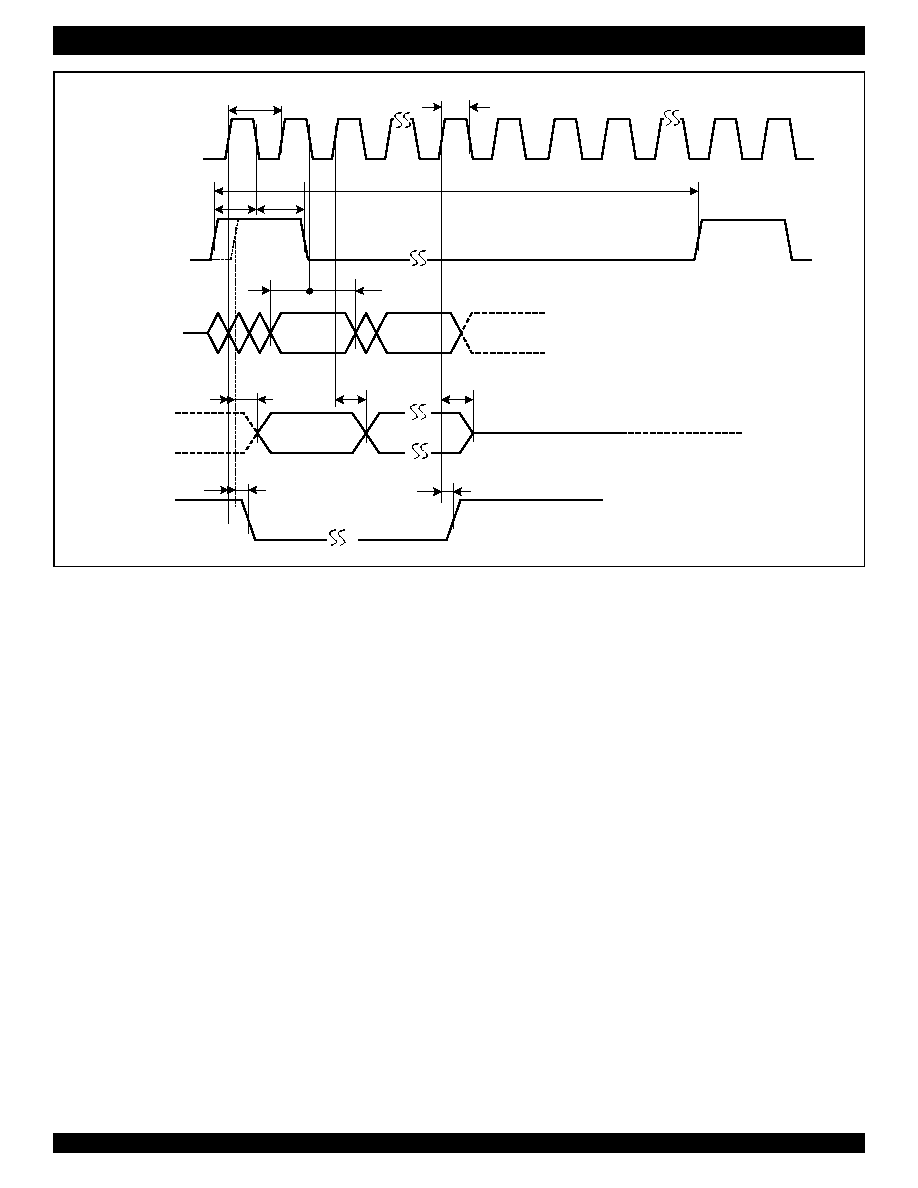
102
RSLIC (IDT82V1671) & CODEC (IDT82V1074) CHIPSET INDUSTRIAL TEMPERATURE RANGE
NOTES:
1) The BCLK frequency must be an integer multiple of the FSC frequency. The maximum BCLK frequency is 8.192 MHz. The minimum BCLK frequency is 64 kHz in compressed mode
and 128 kHz in linear mode if only one channel is used. The minimum BCLK frequency is 256 kHz in compressed mode and 512 kHz in linear mode if all four channels are used.
2) TSX1 or TSX2 typically delays from the FSC for 8
N t22 ns in compressed mode and 16 N t22 ns in linear mode, where N is the specified time slot (value of TT[6:0] in register
LREG1).
3) t33 is defined to be the time when the TSX1 or TSX2 output achieves high level.
4)
Figure - 46
and
Figure - 47
show the timing of transmit at the rising edges of BCLK and receive at the falling edges of it.
∑
Figure - 47 PCM Interface Timing (Double Clock Mode)
t25
t26
t22
t23
t27
t28
first bit
t29
t30
t31
BCLK
FSC
DR1/DR2
DX1/DX2
t32
t33
t24
High Z
TSX1/TSX2
first bit
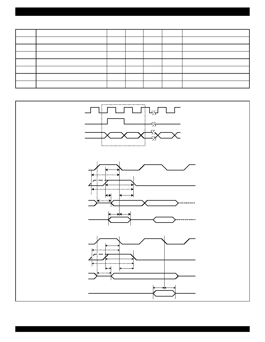
103
RSLIC (IDT82V1671) & CODEC (IDT82V1074) CHIPSET INDUSTRIAL TEMPERATURE RANGE
7.4.4
GCI INTERFACE TIMING
∑
∑
Symbol
Description
Min.
Typ.
Max.
Units
Test Conditions
t34
FSC rise and fall time
60
ns
t35
FSC setup time
70
t9
- 50
ns
t36
FSC hold time
50
ns
t37
FSC high pulse width
130
ns
t38
DU data delay time
100
ns
t39
DD data delay time
110
ns
t40
DD data hold time
50
ns
∑
Figure - 48 GCI Interface Timing
DU
DD
FSC
DCL
4.096 MHZ
t35
t36
t37
t38
t38
t39
t40
t35
t37
B7
B7
DU
DD
FSC
DCL
2.048MHz
t35
t36
t37
t38
t38
t39
t40
t35
t37
B7
B6
B7
B6
B7
B6
B0
Detail A
DCL
FSC
DD/DU
Detail A
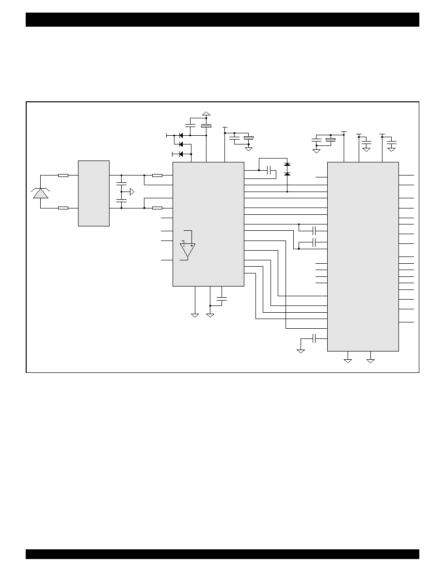
104
RSLIC (IDT82V1671) & CODEC (IDT82V1074) CHIPSET INDUSTRIAL TEMPERATURE RANGE
8
APPLICATION CIRCUITS
8.1
APPLICATION CIRCUIT FOR THE INTERNAL RINGING MODE
The RSLIC-CODEC chipset can provide an internal ringing signal without any external components. The amplitude of the internal ringing signal
can be up to 70 Vp. The off-hook detection and ring trip detection are also internally performed.
Figure - 49
shows an application circuit for the internal
ringing mode.
Figure - 49 Application Circuit for the Internal Ringing Mode
IDT82V1671
VBH
VBL
VDD
TIS
TIP
RING
RIS
VCMB
RSP
RSN
RT
AGND
BGND CF
M3
M2
M1
CS
VCM
DCP
DCN
VTDC
VTAC
VL
CA
IDT82V1074
(Channel1)
VDDD
VDDA
VDDB
RTIN1
VL1
VTAC1
VTDC1
ACN1
DCN1
CA2_1
DCP1
GNDA
GNDD
FSC
DCL/BCLK
INT/INT
MCLK
RESET
CO
CI/S1
CCLK/S0
CS
MPI/GCI
ACP1
CA1_1
IO1_1
IO2_1
IO3_1
IO4_1
CS1
M1
M2
M3
CNF
VCM
TSX1
DX1/DU
DR1/DD
TSX2
DX2
DR2
RSYNC
ACN
ACP
14
16
13
15
9
10
11
12
8
21
20
19
18
52
15
17
56
55
54
47
48
49
50
36
37
38
39
CA1
CA2
40
41
33
34
32
31
+3.3VD
+3.3VA
+3.3VA
60
61
62
63
64
67
66
77
76
75
68
69
70
72
73
74
59
+3.3V
VBL
VBH
22
23
24
25
2
26
27
4
1
28
5
6
3
7
CF
PROTECTION
C
INT
R
S
C
STAB
C
STAB
R
PROT
R
S
R
PROT
BGND
+
+
0.1
µF
AGND
10
µF
0.1
µF
10
µF
CB
17
0.1
AGND
AGND
DGND
+
10
µF
0.1
µF
DGND
AGND
AGND
0.1
µF
0.1
µF
AGN
D
AGND
BGND
CNF
D1 (1 A/200 V)
D2 (1 A/200 V)
D3 (1 A/200 V)
D4
1N4148
D5
1N4148

105
RSLIC (IDT82V1671) & CODEC (IDT82V1074) CHIPSET INDUSTRIAL TEMPERATURE RANGE
8.2
APPLICATION CIRCUIT FOR THE EXTERNAL RINGING MODE
The chipset also supports the external ringing mode.
Figure - 50
shows an application circuit for the external ringing mode.
Figure - 50 Application Circuit for the External Ringing Mode
Table - 28 External Components in Application Circuits
Symbol
Value
Unit
Tolerance
Rating
R
PROT
50
±5%
1 W
R
S
50
±1%
1 W
R1, R2
100
k
±10%
R3, R6
150
±10%
1 W
R4, R5, R7, R8
10
±10%
C
STAB
22
nF
±10%
100 V
C
INT
0.47
µF
±10%
50 V
CA1
0.047
µF
±10%
CA2
0.047
µF
±10%
CF
0.47
µF
±10%
50 V
CNF
0.1
µF
±10%
C1, C2
1
µF
±10%
IDT82V1671
VBH
VBL
VDD
TIS
TIP
RING
RIS
VCMB
RSN
RSP
RT
AGND
BGND CF
M3
M2
M1
CS
VCM
DCP
DCN
VTDC
VTAC
VL
IDT82V1074
(Channel1)
VDDD VDDA
VDDB
RTIN1
VL1
VTAC1
VTDC1
ACN1
DCN1
CA2_1
DCP1
GNDA
GNDD
FSC
DCL/BCLK
INT/INT
MCLK
RESET
CO
CI/S1
CCLK/S0
CS
MPI/GCI
ACP1
CA1_1
IO1_1
IO2_1
IO3_1
IO4_1
CS1
M1
M2
M3
CNF
VCM
TSX1
DX1/DU
DR1/DD
TSX2
DX2
DR2
RSYNC
ACN
ACP
16
13
15
9
10
11
12
8
21
20
19
18
52
15
17
56
55
54
47
48
49
50
36
37
38
39
CA1
CA2
40
41
33
34
32
31
22
24
23
25
2
26
27
4
6
3
7
CF
PROTECTION
R
S
C
STAB
R
PROT
R
S
R
PROT
CNF
+5V
Ring
Generator
-48V DC
80Vrms
AGND
BGND
C
STAB
BGND
AGND
DGND
AGND
Relay
+3.3V
VBL
VBH
1
28
5
+
+
0.1
µF
AGND
10
µF
0.1
µF
10
µF
CA 14
CB 17
AGN
D
+3.3VD +3.3VA
+3.3VA
+
10
µF
0.1
µF
DGND
AGND
AGND
0.1
µF
0.1
µF
60
61
62
63
64
67
66
77
76
75
68
69
70
72
73
74
59
IN4148
IN4148
C1
C2
R1
R2
R3
R4
R5
R6
R7
R8
C
INT
D4
D1 (1 A/200 V)
D2 (1 A/200 V)
D3 (1 A/200 V)
1N4148
D5
1N4148
D6
D7
106
RSLIC (IDT82V1671) & CODEC (IDT82V1074) CHIPSET INDUSTRIAL TEMPERATURE RANGE
9
ORDERING INFORMATION
RSLIC (IDT82V1671):
CODEC (IDT82V1074):
IDT
XXXXXXX
X
X
Dev ice Ty pe
Blank
Process/
Temperature
Range
J
82V1671
Industrial (-40 ∞C to +85 ∞C)
Plastic Leaded Chip Carrier (PLCC, PL28)
Ringing SLIC
Package
IDT
XXXXXXX
XX
X
Dev ice Ty pe
Blank
Process/
Temperature
Range
PF
82V1074
Industrial (-40 ∞C to +85 ∞C)
Thin Quad Flat Pack (TQFP, PK100)
Quad Programmable PCM CODEC
Package

107
CORPORATE HEADQUARTERS
2975 Stender Way
Santa Clara, CA 95054
for SALES:
800-345-7015 or 408-727-6116
fax: 408-492-8674
www.idt.com
for Tech Support:
email: telecomhelp@idt.com
phone: 408-330-1
552
RSLIC (IDT82V1671) & CODEC (IDT82V1074) CHIPSET INDUSTRIAL TEMPERATURE RANGE
Data Sheet Document History
11/05/2002
pgs. 1, 17, 36, 44 - 48, 60, 63, 77 - 78, 83 - 85, 88, 94, 103, 104
01/09/2003
pgs. 1, 105
02/28/2003
pgs. 29, 66, 93, 103, 104
04/22/2003
pgs. 73, 93, 94
11/18/2003
pgs. 1, 19, 21, 29, 61, 63, 75
02/16/2004
pgs. 18, 19, 21, 26, 29, 60, 61, 63, 73, 75, 77, 83-85, 93, 94