
T1 / E1 / J1 OCTAL FRAMER
IDT82V2108
PRELIMINARY
The IDT logo is a registered trademark of Integrated Device Technology, Inc.
INDUSTRIAL TEMPERATURE RANGES
1
JANUARY 2003
DSC-6039/3
©
2001 Integrated Device Technology, Inc.
FEATURES
∑
Octal Framer supporting T1, E1 and J1 Formats
∑
Provides programmable system interface to support Mitel
ģ
ST-
bus, AT&T
ģ
CHI and MVIP bus, supporting data rates of 1.544 /
2.048 / 8.192Mb/s; up to four links can be byte interleaved on one
system bus without external logic
∑
Provides up to three internal floating HDLC controllers for each
framer to support ISDN PRI and V5.X interface. Each HDLC con-
tains 128-byte deep FIFOs in both the receive and transmit direc-
tions
∑
Provides jitter attenuation performance exceeding the requirements
set by the associated standards for both Rx and Tx path
∑
Provides payload, line and digital loop-backs
∑
Provides a floating Pseudo Random Bit Sequence / repetitive pat-
tern generator/detector, which can be assigned to any one of eight
framers, the pattern may be inserted / detected in an unframed or
Nx64K or Nx56K (T1 only) basis
∑
Provides signaling insertion / extraction for CCS / CAS and RBS
signaling system
∑
Provides programmable codes insertion, data / sign inversion and
digital milliwatt code insertion on a per channel / timeslot basis
∑
Supports automatic / manual alarming transmit and integration
∑
Provides performance monitor to counter CRC error, framing bit er-
ror, far end block CRC error (E1), out of frame event (T1/J1) and
change of frame alignment event (T1/J1)
∑
Provides programmable In-band Loop-back Code transmitter/re-
ceiver, Bit Oriented Message generator / detector
∑
Supports polled or interrupt driven processing for all events
∑
Supports multiplexed or non-multiplexed address/data bus MPU in-
terface for configuration, control and status monitoring
∑
JTAG boundary scan meets IEEE 1149.1
∑
Low power 3.3V CMOS technology with 5V tolerant inputs
∑
Operating industrial temperature range: -40
į
C to +85
į
C
∑
Package available: 128 pin PQFP
144 pin PBGA
APPLICATIONS
∑
High density internet E1 or T1 / J1 interface for routers, multiplex-
ers, switches and digital modems.
∑
Frame relay switches and access devices (FRADS)
∑
SONET / SDH add drop multiplexers
∑
Digital private branch exchanges (PBX)
∑
Channel service units (CSU) and data service units (DSU)
∑
Channel banks and multiplexers
∑
Digital access and cross-connect systems (DACS)
STANDARDS
E1 MODE:
ITU-T: G.704, G.706, G.732, G.802, G.737, G.738, G.739, G.742,
G.823, G.964, G.965, I.431, O.151, O.152, O.153;
ETSI: ETS 300 011, ETS 300 233, ETS 324-1, ETS 347-1, TBR 4,
TBR 12, TBR 13;
GO - MVIP
T1/J1 MODE:
ANSI: T1.107, T1.231, T1.403, T1.408;
TR: TSY-000147, TSY-000191, NWT-000303, TSY-000312, TSY-000-
499;
AT&T: TR 54016, TR 62411
TTC: JT-G 703, JT-G 704, JT-G706, JT-G 1431

2
INDUSTRIAL
TEMPERATURE RANGES
IDT82V2108 T1 / E1 / J1 OCTAL FRAMER
DESCRIPTION
The IDT82V2108 is a flexible feature-rich octal T1/E1/J1 Framer.
Controlled by the software, the IDT82V2108 can be globally configured
as an Octal E1 or T1/J1 Framer. When E1 or T1/J1 has been set glo-
bally, the operation mode of each of the eight framers can be
configured independently. The configuration is performed through a par-
allel Multiplexed/Non-Multiplexed microprocessor interface.
The IDT82V2108 realizes frame synchronization, frame generating,
signaling extraction and insertion, alarm and test signals generation
and detection in a single chip. It also integrates up to three HDLC re-
ceivers and HDLC transmitters for each of the eight framers.
In E1 Mode, the receive path of each framer can be configured to
frame to Basic Frame, CRC Multi-Frame and Signaling Multi-Frame.
The framing can also be bypassed (unframed mode). It detects and
indicates the event of out of Basic Frame Sync, out of CRC Multi-
Frame, out of Signaling Multi-Frame, the Remote Alarm Indication
signal and the Remote Signaling Multi-Frame Alarm Indication signal. It
also monitors the Red and AIS alarms. Basic Frame Alignment Signal
errors, Far End Block Errors (FEBE) and CRC errors are counted. Up
to three HDLC links are provided to extract the HDLC message on
TS16, the Sa National bits and/or any arbitrary timeslot. An Elastic
Store Buffer that optionally supports slip buffering and adaptation to
backplane timing is provided. In E1 receive path, signaling debounce,
signaling freezing, idle code substitution, digital milliwatt code insertion,
trunk conditioning, data inversion and pattern generation or detection
are also supported on a per-timeslot basis.
In E1 mode, the transmit path of each framer can be configured to
generate Basic Frame, CRC Multi-Frame and Signaling Multi-Frame.
The framing can also be disabled (unframed mode). It can also transmit
Remote Alarm Indication signal, the Remote Signaling Multi-Frame
Alarm Indication signal, AIS signal and FEBE. Up to three HDLC links
are provided to insert the HDLC message on TS16, the Sa National bits
and/or any arbitrary timeslot. The signaling insertion, idle code
substitution, data insertion, data inversion and test pattern generation
or detection are also supported on a per-timeslot basis.
In E1 mode, any four of the eight framers can be multiplexed or de-
multiplexed to or from one of the two 8.192M bit/s buses.
In T1/J1 mode, the receive path of each framer can be configured to
frame to Super Frame (SF) or Extended Super Frame (ESF) formats.
The framing can also be bypassed (unframed mode). It detects and
indicates the out of SF/ESF sync event, the Yellow, Red and AIS
alarms. It also detects the presence of inband loopback codes, bit
oriented message. Frame Alignment Signal errors, CRC-6 errors, out of
SF/ESF events and Frame Alignment position changes are counted. Up
to two HDLC links are provides to extract the HDLC message on the F-
bit or any arbitrary channels in ESF mode. An Elastic Store Buffer that
optionally supports controlled slip and adaptation to backplane timing is
provided. In T1/J1 receive path, signaling debounce, signaling freezing,
idle code substitution, digital milliwatt code insertion, idle code insertion,
data inversion and pattern generation or detection are also supported
on a per-channel basis.
In T1/J1 mode, the transmit path of each framer can be configured
to generates SF or ESF. The framing can also be disabled (unframed
mode). It can also transmit Yellow signal and AIS signal. Inband
loopback codes and bit oriented message can also be transmitted. Up
to two HDLC links are provided to insert the HDLC message on the F-
bit or any arbitrary channels in ESF mode. The signaling insertion, idle
code substitution, data insertion, data inversion and test pattern
generation or detection are also supported on a per-channel basis.
In T1/J1 mode, the data stream of 1.544M bit/s can be converted to/
from the data stream of 2.048M bit/s on the system side by software
configuration. In addition, any four of the eight framers can be
multiplexed or de-multiplexed to or from one of the two 8.192M bit/s
buses.
3
INDUSTRIAL
TEMPERATURE RANGES
IDT82V2108 T1 / E1 / J1 OCTAL FRAMER
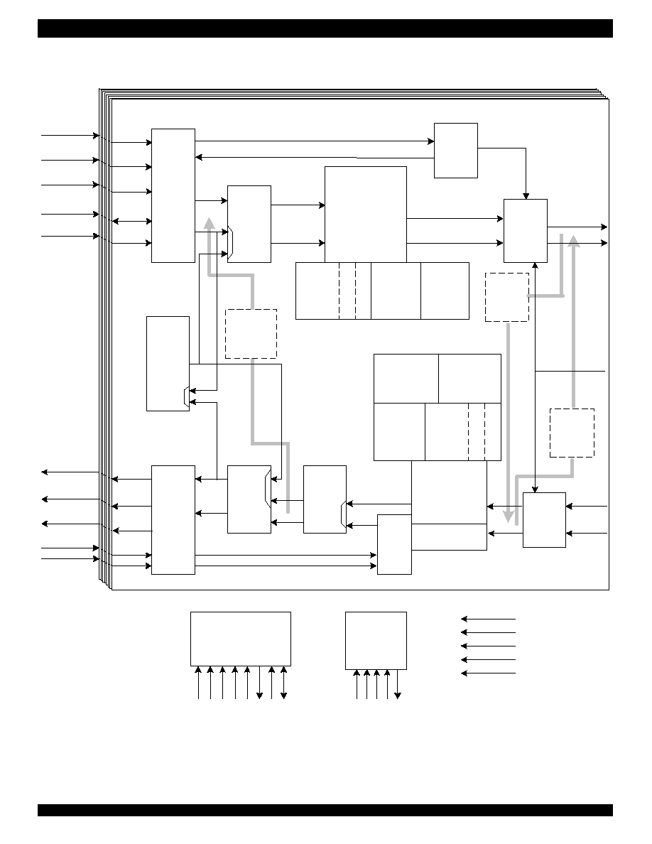
Micro-Processor
Interface
D[7:0]
RST
INT
ALE
CS
WR
RD
A[10:0]
Receive
System
Interface
RSFSn
RSCKn/
RSSIGn
RSDn
Receive
Payload
Control
Receive
CAS/RBS
Buffer
Elastic
Store
Buffer
Frame Processor
Receive
Jitter
Attenuator
LRCKn
LRDn
HDLC
Receiver #1
Inband
Loopback
Code Detector
(T1/J1 only)
IEEE1149.1
JTAG
TRST TMS
TCLK
TDI
TDO
PRBS
Generator
/Detector
Transmit
System
Interface
Transmit
Payload
Control
Frame Generator
Transmit
Jitter
Attenuator
Transmit
Clock
Inband
Loopback
Code
Generator
(T1/J1 only)
RSCFS/
MRSCFS
RSCCK/
MRSCCK
TSFSn/
TSSIGn
TSCFS/
MTSCFS
TSDn
TSCCKB/
MTSCCKB
TSCCKA
One of the Eight Framers
LTCKn
LTDn
XCK
#2
#3
(E1
only)
HDLC
Transmitter
#1
#2
#3
(E1
only)
Payload
Loopback
Digital
Loopback
Line
Loopback
MRSFS[1:2]
MRSSIG[1:2]
MRSD[1:2]
MTSD[1:2]
MTSSIG[1:2]
BIAS
VDDIO
VDDC
GNDIO
GNDC
Performance
Monitor
Alarm
Detector
(T1/J1 only)
Bit-Oriented
Message
Receiver
(T1/J1 only)
Bit-Oriented
Message
Transmitter
(T1/J1 only)
FUNCTIONAL BLOCK DIAGRAM

4
INDUSTRIAL
TEMPERATURE RANGES
IDT82V2108 T1 / E1 / J1 OCTAL FRAMER
CONTENTS
1 PIN ASSIGNMENTS ............................................................................................................................................ 13
1.1 128 PIN PQFP PACKAGE (TOP VIEW) .................................................................................................................................................. 13
1.2 144 PIN PBGA PACKAGE (BOTTOM VIEW) .......................................................................................................................................... 14
2 PIN DESCRIPTION .............................................................................................................................................. 15
3 FUNCTIONAL DESCRIPTION .............................................................................................................................. 21
3.1 T1 / E1 / J1 MODE SELECTION ............................................................................................................................................................. 21
3.2 FRAME PROCESSOR (FRMP) ............................................................................................................................................................... 21
3.2.1 E1 Mode ......................................................................................................................................................................................... 21
3.2.2 T1/J1 Mode .................................................................................................................................................................................... 26
3.3 PERFORMANCE MONITOR (PMON) ..................................................................................................................................................... 28
3.3.1 E1 Mode ......................................................................................................................................................................................... 28
3.3.2 T1/J1 Mode .................................................................................................................................................................................... 28
3.4 ALARM DETECTOR (ALMD) - T1 / J1 ONLY .......................................................................................................................................... 28
3.5 HDLC RECEIVER (RHDLC) ................................................................................................................................................................... 29
3.5.1 E1 Mode ......................................................................................................................................................................................... 29
3.5.2 T1 / J1 Mode .................................................................................................................................................................................. 30
3.6 BIT-ORIENTED MESSAGE RECEIVER (RBOM) - T1 / J1 ONLY............................................................................................................. 30
3.7 INBAND LOOPBACK CODE DETECTOR (IBCD) - T1 / J1 ONLY ........................................................................................................... 31
3.8 ELASTIC STORE BUFFER (ELSB) ........................................................................................................................................................ 31
3.8.1 E1 Mode ......................................................................................................................................................................................... 31
3.8.2 T1 / J1 Mode .................................................................................................................................................................................. 31
3.9 RECEIVE CAS/RBS BUFFER (RCRB) ................................................................................................................................................... 31
3.9.1 E1 Mode ......................................................................................................................................................................................... 31
3.9.2 T1 / J1 Mode .................................................................................................................................................................................. 33
3.10 RECEIVE PAYLOAD CONTROL (RPLC) .............................................................................................................................................. 33
3.10.1 E1 Mode ....................................................................................................................................................................................... 33
3.10.2 T1 / J1 Mode ................................................................................................................................................................................ 34
3.11 RECEIVE SYSTEM INTERFACE (RESI) ............................................................................................................................................... 35
3.11.1 E1 Mode ....................................................................................................................................................................................... 35
3.11.1.1 Receive Clock Slave Mode .................................................................................................................................................... 36
3.11.1.1.1 Receive Clock Slave RSCK Reference Mode ........................................................................................................ 36
3.11.1.1.2 Receive Clock Slave External Signaling Mode ...................................................................................................... 38
3.11.1.2 Receive Clock Master Mode ................................................................................................................................................... 39
3.11.1.2.1 Receive Clock Master Full E1 Mode ..................................................................................................................... 39
3.11.1.2.2 Receive Clock Master Fractional E1 (with F-bit) Mode ........................................................................................... 41
3.11.1.3 Receive Multiplexed Mode ..................................................................................................................................................... 41
3.11.1.4 Parity Check & Polarity Fix ..................................................................................................................................................... 43
3.11.1.5 Offset .................................................................................................................................................................................... 44
3.11.1.6 Output On RSDn/MRSD & RSSIGn/MRSSIG ......................................................................................................................... 44

5
INDUSTRIAL
TEMPERATURE RANGES
IDT82V2108 T1 / E1 / J1 OCTAL FRAMER
3.11.2 T1 / J1 Mode ................................................................................................................................................................................ 47
3.11.2.1 Receive Clock Slave Mode .................................................................................................................................................... 47
3.11.2.1.1 Receive Clock Slave RSCK Reference Mode ........................................................................................................ 48
3.11.2.1.2 Receive Clock Slave External Signaling Mode ...................................................................................................... 50
3.11.2.2 Receive Clock Master Mode ................................................................................................................................................... 50
3.11.2.2.1 Receive Clock Master Full T1/J1 Mode ................................................................................................................. 52
3.11.2.2.2 Receive Clock Master Fractional T1/J1 Mode ....................................................................................................... 52
3.11.2.3 Receive Multiplexed Mode ..................................................................................................................................................... 52
3.11.2.4 Parity Check .......................................................................................................................................................................... 53
3.11.2.5 Offset .................................................................................................................................................................................... 55
3.11.2.6 Output On RSDn/MRSD & RSSIGn/MRSSIG ......................................................................................................................... 55
3.12 PRBS GENERATOR / DETECTOR (PRGD) .......................................................................................................................................... 56
3.12.1 E1 Mode ....................................................................................................................................................................................... 56
3.12.2 T1 / J1 Mode ................................................................................................................................................................................ 57
3.13 TRANSMIT SYSTEM INTERFACE (TRSI) ............................................................................................................................................. 57
3.13.1 E1 Mode ....................................................................................................................................................................................... 57
3.13.1.1 Transmit Clock Slave Mode ................................................................................................................................................... 58
3.13.1.1.1 Transmit Clock Slave TSFS Enable Mode ........................................................................................................... 58
3.13.1.1.2 Transmit Clock Slave External Signaling Mode ................................................................................................... 60
3.13.1.2 Transmit Clock Master Mode .................................................................................................................................................. 61
3.13.1.3 Transmit Multiplexed Mode .................................................................................................................................................... 61
3.13.1.4 Parity Check .......................................................................................................................................................................... 63
3.13.1.5 Offset .................................................................................................................................................................................... 65
3.13.2 T1 / J1 Mode ................................................................................................................................................................................ 68
3.13.2.1 Transmit Clock Slave Mode ................................................................................................................................................... 68
3.13.2.1.1 Transmit Clock Slave TSFS Enable Mode ........................................................................................................... 69
3.13.2.1.2 Transmit Clock Slave External Signaling Mode ................................................................................................... 71
3.13.2.2 Transmit Clock Master Mode .................................................................................................................................................. 72
3.13.2.3 Transmit Multiplexed Mode .................................................................................................................................................... 72
3.13.2.4 Parity Check .......................................................................................................................................................................... 75
3.13.2.5 Offset .................................................................................................................................................................................... 75
3.14 TRANSMIT PAYLOAD CONTROL (TPLC) ............................................................................................................................................ 76
3.14.1 E1 Mode ....................................................................................................................................................................................... 76
3.14.2 T1 / J1 Mode ................................................................................................................................................................................ 76
3.15 FRAME GENERATOR (FRMG) ............................................................................................................................................................. 77
3.15.1 E1 Mode ....................................................................................................................................................................................... 77
3.15.2 T1 / J1 Mode ................................................................................................................................................................................ 78
3.16 HDLC TRANSMITTER (THDLC) ........................................................................................................................................................... 79
3.16.1 E1 Mode ....................................................................................................................................................................................... 79
3.16.2 T1 / J1 Mode ................................................................................................................................................................................ 79
3.17 BIT-ORIENTED MESSAGE TRANSMITTER (TBOM) - T1 / J1 ONLY .................................................................................................... 80
3.18 INBAND LOOPBACK CODE GENERATOR (IBCG) - T1 / J1 ONLY ...................................................................................................... 80