COMMERCIAL TEMPERATURE RANGE
IDTCV115C
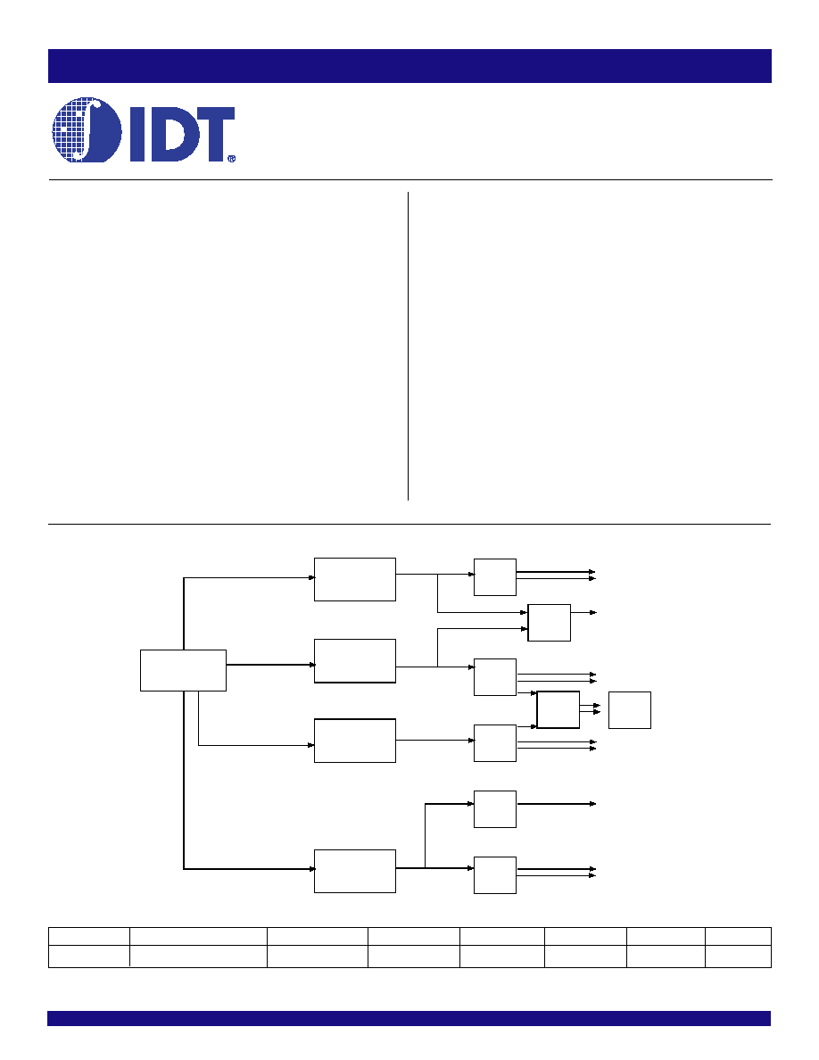
PROGRAMMABLE FLEXPCTM CLOCK FOR P4 PROCESSOR
1
MAY 2004
IDTCV115C
COMMERCIAL TEMPERATURE RANGE
PROGRAMMABLE FLEXPCTM
CLOCK FOR P4 PROCESSOR
SATA PLL
SCC
Programmable
SATA/
CPU[1:0]
SRC[6:5] [3:1]
USB48
DOT96
PCI[4:0], PCIF[2:0]
SRC4 - SATA
PCI/
PCIE/
Host/
48MHz/
96MHz/
MUX
PCIEX PLL
SCC
N Programmable
CPU PLL
SCC
N Programmable
Fixed PLL
No SCC
14.318MHz
Osc
CPU_ITP/
SRC7
The IDT logo is a registered trademark of Integrated Device Technology, Inc.
� 2004 Integrated Device Technology, Inc.
DSC - 6520/10
FEATURES:
� One high precision N and SSC programmable PLL for SRC/PCI
� One high precision N and SSC programmable PLL for CPU
� One high precision SSC programmable PLL for SATA
� One high precision PLL for 96MHz/48MHz
� Band-gap circuit for differential outputs
� Support multiple spread spectrum modulation, down and
center
� Support SMBus block read/write, index read/write
� Selectable output strength for REF, PCI, and USB48MHz
� Available in SSOP package
FUNCTIONAL BLOCK DIAGRAM
DESCRIPTION:
IDTCV115C is a 56 pin clock device, complying the latest Intel CK410
requirements, for Intel advance P4 processors. The CPU output buffer is
designed to support up to 400MHz processor. One dedicated PLL for Serial
ATA clock provides high accuracy frequency. This device also implements
Band-gap referenced I
REF
to reduce the impact of V
DD
variation on differential
outputs, which can provide more robust system performance.
Each CPU/SRC/PCI, SATA clock has its own Spread Spectrum selection,
which allows for isolated changes instead of affecting other clock groups.
KEY SPECIFICATION:
� CPU/SRC CLK cycle to cycle jitter < 85ps
� SATA CLK cycle to cycle jitter < 85ps
� Static PLL frequency divide error < 114 ppm
� Static PLL frequency divide error for 48MHz < 5 ppm
OUTPUT TABLE
CPU
CPU_ITP/SRC
SRC
SATA
PCI/PCIF
REF
DOT96
48MHz
2
1
5
1
8
1
1
1
COMMERCIAL TEMPERATURE RANGE
2
IDTCV115C
PROGRAMMABLE FLEXPCTM CLOCK FOR P4 PROCESSOR
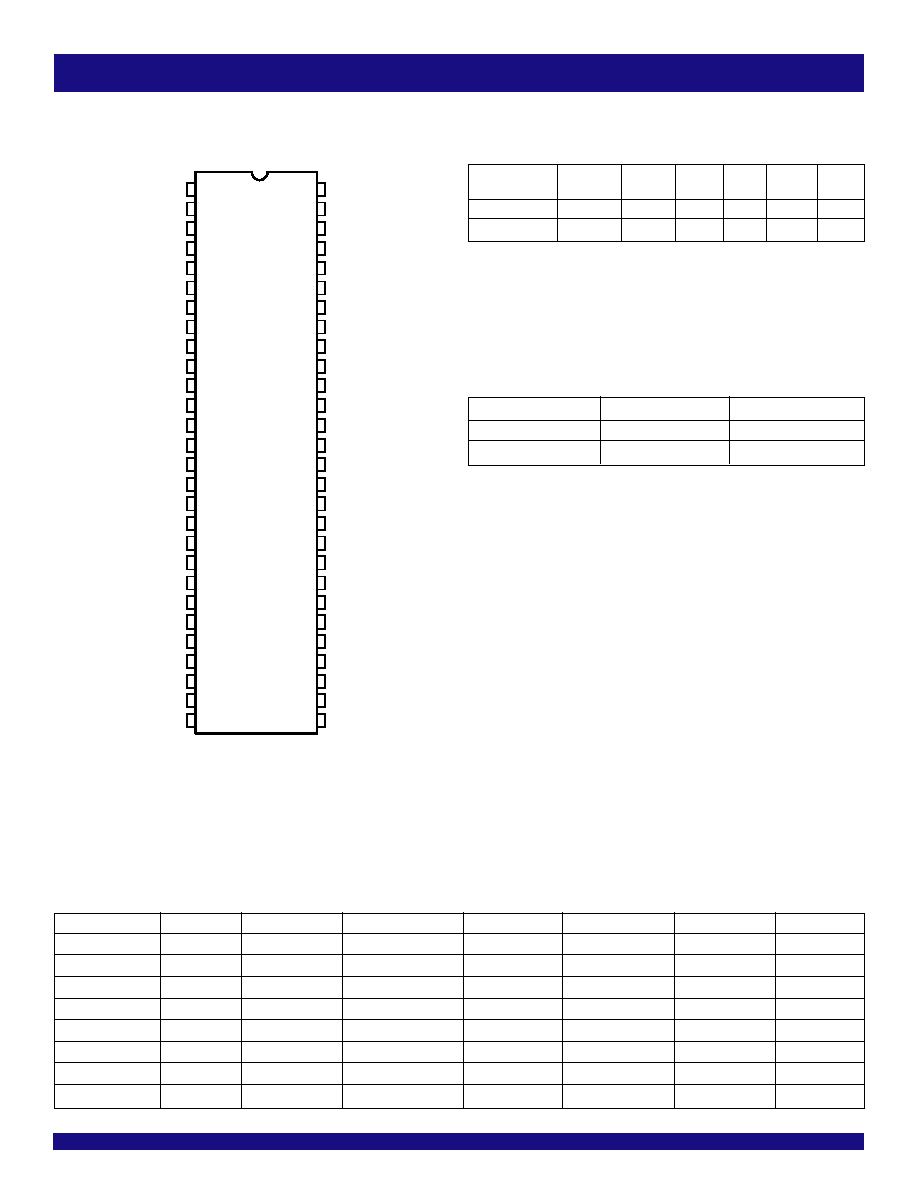
PIN CONFIGURATION
SSOP
TOP VIEW
56
55
54
53
52
51
50
49
48
47
46
45
44
43
42
41
40
39
38
37
36
35
34
33
32
31
30
29
PCI1
PCI0
FS_A
REF0
V
SS
_REF
XTAL_IN
XTAL_OUT
V
DD
_REF
SCL*
SDA*
CPUT0
CPUC0
V
DD
_CPU
CPUT1
CPUC1
I
REF
FS_B/Test_Mode
CPU2_ITP/SRCT7
CPU2_ITP/SRCC7
V
DD
_SRC
SRCC6
SRCT5
SRCC5
V
SS
_SRC
1
2
3
4
5
6
7
8
9
10
11
12
13
14
15
16
17
18
19
20
21
22
23
24
25
26
27
28
V
DD
_PCI
V
SS
_PCI
PCI2
PCI3
PCI4
V
SS
_PCI
V
DD
_PCI
PCIF
0
/ITP
_
EN
PCIF1
**V
TT
_P
WRGD#
/
P
WRDWN
V
DD_
48
USB48MHz
V
SS_
48
DOT_96
DOT_96#
PCIF2
SRCT1
SRCC1
V
DD
_SRC
SRCT2
SRCC2
SRCT3
SRCC3
SRCT4_SATA
V
DD
_SRC
SRCT6
V
SS
V
SS_
GND
SRCC4_SATA
V
DD
_suspend
V
SS
_CPU
FS_C/Test _Sel
HW FREQUENCY SELECTION TABLE
FSC, B, A
CPU
SRC4_SATA
SRC[3:1], SCR[7:5]
PCI
USB
DOT
REF
101
100
100
100
33.3
48
96
14.318
001
133
100
100
33.3
48
96
14.318
011
166
100
100
33.3
48
96
14.318
010
200
100
100
33.3
48
96
14.318
000
266
100
100
33.3
48
96
14.318
100
333
100
100
33.3
48
96
14.318
110
400
100
100
33.3
48
96
14.318
111
Reserve
100
100
33.3
48
96
14.318
* = ~ 130K
internal pull-up.
** = ~ 130K
internal pull-down.
TEST MODE SELECT
(1)
If TEST_SEL sampled above 2V at V
TT
_P
WRGD
active LOW
Pin38
(test_mode)
CPU
SRC
PCI/F
REF
DOT96
USB
1
REF/N
REF/N
REF/N REF
REF/N
REF/N
0
Hi-Z
Hi-Z
Hi-Z
Hi-Z
Hi-Z
Hi-Z
NOTE:
1. Once test clock operation has been invoked, TEST_MODE pin will select between
the Hi-Z and REF/N.
ITP_EN
pin 38
pin 39
1
CPUC2_ITP
CPUT_ITP
0
SRCC7
SRCT7
ITP_EN

COMMERCIAL TEMPERATURE RANGE
IDTCV115C
PROGRAMMABLE FLEXPCTM CLOCK FOR P4 PROCESSOR
3
PIN DESCRIPTION
Pin Number
Name
Type
Description
1
V
DD
_PCI
PWR
3.3V
2
V
SS
_PCI
GND
GND
3
PCI2
OUT
PCI clock
4
PCI3
OUT
PCI clock
5
PCI4
OUT
PCI clock
6
V
SS
_PCI
GND
GND
7
V
DD
_PCI
PWR
3.3V
8
PCIF0/ITP_EN
I/0
PCI clock, free running. CPU_2 select (sampled at V
TT
_P
WRGD
# assertion), HIGH = CPU_2.
9
PCIF1
OUT
PCI clock,
10
PCIF2
OUT
PCI clock,
11
V
DD
_48
PWR
3.3V
12
USB48
OUT
48MHz clock
13
V
SS
_48
GND
GND
14
DOT_96T
OUT
96MHz 0.7V current mode differential clock output
15
DOT_96C
OUT
96MHz 0.7V current mode differential clock output
16
**V
TT
_P
WRGD
#/P
WRDWN
I/O
3.3V LVTTL input is a level-sensitive strobe used to latch the FS_A, FS_B, FS_C/TEST_SEL and
PCIF_0/ITP_EN inputs. After V
TT
_P
WRGD
# assertion, becomes a real-time input for asserting power
down (active high). Internal pull LOW.
17
SRCT1
OUT
Differential Serial reference clock
18
SRCC1
OUT
Differential Serial reference clock
19
V
DD
_SRC
PWR
3.3V
20
V
SS
GND
GND
21
SRCT2
OUT
Differential Serial reference clock
22
SRCC2
OUT
Differential Serial reference clock
23
SRCT3
OUT
Differential Serial reference clock
24
SRCC3
OUT
Differential Serial reference clock
25
V
SS
GND
GND
26
SRCT4_SATA
OUT
SATA clock
27
SRCC4_SATA
OUT
SATA clock
28
V
DD
_SRC
PWR
3.3V
29
V
SS
_SRC
GND
GND
30
SRCC5
OUT
Differential Serial reference clock
31
SRCT5
OUT
Differential Serial reference clock
32
SRCC6
OUT
Differential Serial reference clock
33
SRCT6
OUT
Differential Serial reference clock
34
V
DD
_SRC
PWR
3.3V
35
CPUC2_ITP/ SRCC7
OUT
Selectable CPU or SRC differential clock output. ITP_EN=0 @ V
TT
_P
WRGD
# assertion = SRC_7
36
CPUT2_ITP/ SRCT7
OUT
Selectable CPU or SRC differential clock output. ITP_EN=0 @ V
TT
_P
WRGD
# assertion = SRC_7
37
FS_C/Test_Sel
I/O
CPU frequency selection. Selects test mode if pulled above 2V when V
TT
_P
WRGD
# is asserted.
38
FS_B/ Test_Mode
I/O
CPU frequency selection. In test mode, 1=Hi-Z, 0=REF/N.
39
IREF
OUT
Reference current for differential output buffer
40
V
SS
GND
GND
41
CPUC1
OUT
Host 0.7V current mode differential clock output
42
CPUT1
OUT
Host 0.7V current mode differential clock output
43
V
DD
_CPU
PWR
3.3V
44
CPUC0
OUT
Host 0.7V current mode differential clock output
45
CPUT0
OUT
Host 0.7V current mode differential clock output
46
*SDA
I/O
SMBus data
COMMERCIAL TEMPERATURE RANGE
4
IDTCV115C
PROGRAMMABLE FLEXPCTM CLOCK FOR P4 PROCESSOR
PIN DESCRIPTION (CONT.)
Pin Number
Name
Type
Description
47
*SCL
IN
SMBus CLK
48
V
DD
_REF
PWR
3.3V
49
XTAL_OUT
OUT
Xtal output
50
XTAL_IN
IN
Xtal input
51
V
SS
_REF
GND
GND
52
REF0
OUT
14.318 MHz reference clock output
53
V
DD
_Suspend
PWR
In the power down mode, supply 3.3V to SM control registers, <1mA. In the normal operation, regular
V
DD
.
54
FS_A
IN
CPU frequency selection
55
PCI0
OUT
PCI clock
56
PCI1
OUT
PCI clock
INDEX BLOCK WRITE PROTOCOL
Bit
# of bits
From
Description
1
1
Master
Start
2-9
8
Master
D2h
10
1
Slave
Ack (Acknowledge)
11-18
8
Master
Register offset byte (starting byte)
19
1
Slave
Ack (Acknowledge)
20-27
8
Master
Byte count, N, (0 is not valid
28
1
Slave
Ack (Acknowledge)
29-36
8
Master
first data byte (Offset data byte)
37
1
Slave
Ack (Acknowledge)
38-45
8
Master
2nd data byte
46
1
Slave
Ack (Acknowledge)
:
Master
Nth data byte
Slave
Acknowledge
Master
Stop
INDEX BLOCK READ PROTOCOL
Master can stop reading any time by issuing the stop bit without waiting
until Nth byte (byte count bit30-37).
Bit
# of bits
From
Description
1
1
Master
Start
2-9
8
Master
D2h
10
1
Slave
Ack (Acknowledge)
11-18
8
Master
Register offset byte (starting byte)
19
1
Slave
Ack (Acknowledge)
20
1
Master
Repeated Start
21-28
8
Master
D3h
29
1
Slave
Ack (Acknowledge)
30-37
8
Slave
Byte count, N (block read back of N
bytes), Byte 8
38
1
Master
Ack (Acknowledge)
39-46
8
Slave
first data byte (Offset data byte)
47
1
Master
Ack (Acknowledge)
48-55
8
Slave
2nd data byte
Ack (Acknowledge)
:
Master
Ack (Acknowledge)
Slave
Nth data byte
Not acknowledge
Master
Stop
INDEX BYTE WRITE
Setting bit[11:18] = starting address, bit[20:27] = 01h.
INDEX BYTE READ
Setting bit[11:18] = starting address. After reading back the first data byte,
master issues Stop bit.
SM PROTOCOL

COMMERCIAL TEMPERATURE RANGE
IDTCV115C
PROGRAMMABLE FLEXPCTM CLOCK FOR P4 PROCESSOR
5
S.E. CLOCK STRENGTH SELECTION (PCI, REF, USB48)
Str[1:0]
Multiple loads
Single loads
USB48
00
2L
Recommend
Recommend
01
1H
Recommend
10
1L
Recommend
11
2H
Recommend
Recommend
SSC MAGNITUDE CONTROL, SMC
SMC[2:0]
%
000
OFF
001
- 0.25
010
- 0.5
011
�0.125
100
�0.25
101
�0.375
110
�0.5
111
�0.75
PCIS[1:0]
PCI
00
33.33
01
36.36
10
40
11
S_CBS[1:0], H_CBS[1:0] BAND
SELECTION
S_CBS/H_CBS[1:0]
00
FS[C,B,A]
01
CB1_[2:0], byte17, CPU PLL Mode selection1
10
CB2_[2:0], byte17, CPU PLL Mode selection2
11
Don't care
PCI
When Byte5 bit6 = 0; otherwise, PCI = SRC frequency/3
S_CNS, S_PNS, H_CNS,H_PNS N
SELECTION
NS[1:0]
00
Standard of Each CPU Mode (Band)
01
N Selection 1
10
N Selection 2
11
Don't care
N Resolution (MHz)
%
N=
CPU = 100MHz mode
0.666667
0.67%
150
CPU = 133MHz mode
0.888889
0.67%
150
CPU = 166MHz mode
1.333333
0.8%
125
CPU = 200MHz mode
1.333333
0.67%
150
CPU = 266MHz mode
2.666667
1.00%
100
CPU = 333MHz mode
2.666667
0.8%
125
CPU = 400MHz mode
2.666667
0.67%
150
SRC (PCI Express)
0.666667
0.67%
150
RESOLUTION
CB1[2:0]. CB2[2:0], CPU MODE
SELECTION
CB[2:0]
CPU Mode, MHz
101
100
001
133
011
166
010
200
000
266
100
333
110
400
111
Reserve