1
INDUSTRIAL TEMPERATURE RANGE
IDTQS34XV245
3.3V HIGH SPEED 32-BIT MULTIWIDTH BUS SWITCH
NOVEMBER 1999
1999 Integrated Device Technology, Inc.
DSC-5580/-
c
IDTQS34XV245
INDUSTRIAL TEMPERATURE RANGE
QUICKSWITCH
Æ
PRODUCTS
3.3V HIGH SPEED 32-BIT
MULTIWIDTHTM BUS SWITCH
DESCRIPTION:
FUNCTIONAL BLOCK DIAGRAM
The QS34XV245 is a set of 32-bit high speed bus switches controlled by
LVTTL-compatible active low enable signal. When closed, the switches exhibit
near zero propagation delay without generating additional ground bounce or
switching noise.
The QS34XV245 is specially designed for direct interface betweeen 3.3V
and 2.5V devices without any external components. When operating from a
3.3V supply, the logic high level at the switch output is clamped to 2.5V when
the switch input signal exceeds 2.5V. This device can be used for switching
2.5V buses without signal attenuation. The ON resistance at 3.3V V
CC
is less
than 5
typical, providing near zero propagation delay through the switch.
Absence of DC path from switch I/O pins to V
CC
or ground makes QS34XV245
an ideal device for hot swapping applications.
The QS34XV245 is characterized for operation from -40
∞
C to +85
∞
C.
B 0
2
INDUSTRIAL TEMPERATURE RANGE
IDTQS34XV245
3.3V HIGH SPEED 32-BIT MULTIWIDTH BUS SWITCH
NC
A
0
A
1
A
2
A
3
GN D
A
10
A
11
A
12
A
13
NC
A
20
A
21
A
22
A
23
GN D
A
24
A
25
GN D
GN D
2
3
4
5
6
7
8
73
74
75
76
77
78
79
80
1
55
54
53
52
51
50
49
48
47
46
45
44
43
42
41
56
9
10
11
12
13
14
15
16
17
18
19
20
21
22
23
24
39
38
37
36
35
34
33
32
31
30
29
28
27
26
40
25
58
59
60
61
62
63
64
65
66
67
68
69
70
71
57
72
Vcc
Vcc
Vcc
Vcc
A
4
A
5
A
6
A
7
A
8
A
9
A
14
A
15
A
16
A
17
A
18
A
19
A
26
A
27
A
28
A
29
A
30
A
31
B
0
B
1
B
2
B
3
B
4
B
5
B
6
B
7
B
10
B
11
B
12
B
13
B
8
B
9
B
14
B
15
B
20
B
21
B
22
B
23
B
16
B
17
B
18
B
19
B
24
B
25
B
26
B
27
B
28
B
29
B
30
B
31
NC
NC
OE
1
OE
2
OE
3
OE
4
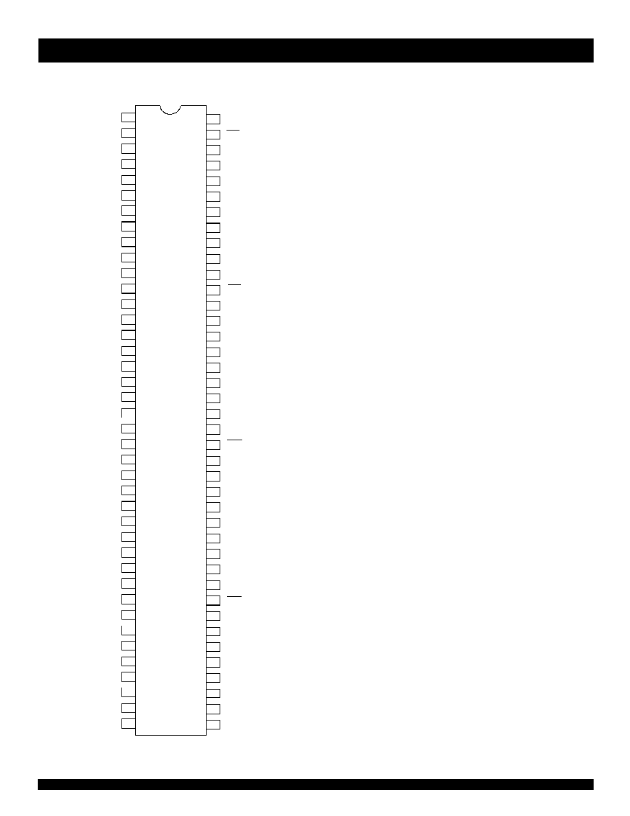
PIN CONFIGURATION

3
INDUSTRIAL TEMPERATURE RANGE
IDTQS34XV245
3.3V HIGH SPEED 32-BIT MULTIWIDTH BUS SWITCH
DC ELECTRICAL CHARACTERISTICS OVER OPERATING RANGE
Following Conditions Apply Unless Otherwise Specified:
Industrial
:
T
A
=
≠
40∞C to +85∞C
,
V
CC
= 3.3V
±
0.3V
Symbol
Parameter
Test Conditions
Min.
Typ.
(1)
Max.
Unit
V
IH
Input HIGH Voltage Level
Guaranteed Logic HIGH for Control Inputs
2
--
--
V
V
IL
Input LOW Voltage Level
Guaranteed Logic LOW for Control Inputs
--
--
0.8
V
I
IN
Input Leakage Current (Control Inputs)
0V
V
IN
V
CC
--
--
1
µ A
I
OZ
Off-State Current (Hi-Z)
0V
V
OUT
V
CC
, Switches OFF
--
0.001
1
µ A
R
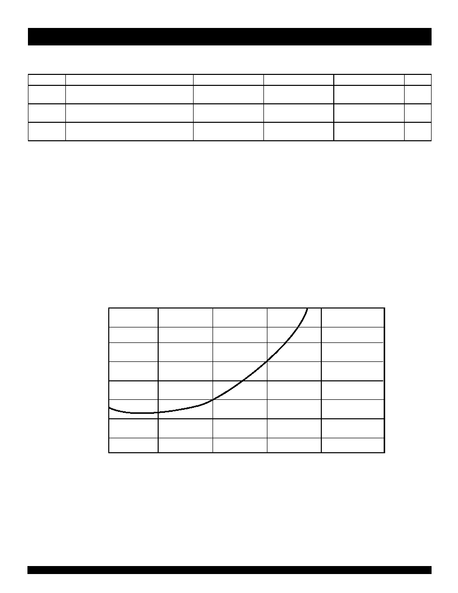
ON
Switch ON Resistance
V
CC
= Min., V
IN
= 0V, I
ON
= 8mA
--
5
7
V
CC
= Min., V
IN
= 1.7V, I
ON
= 8mA
--
15
20
V
CC
= 2.3V, V
IN
= 0V, I
ON
= 8mA
--
7
--
V
CC
= 2.3V, V
IN
= 1.3V, I
ON
= 8mA
--
25
--
V
P
Pass Voltage
(2)
V
IN
=
V
CC
= 3.3V, I
OUT
= -5µ A
2.5
2.7
2.9
V
V
IN
=
V
CC
= 2.5V, I
OUT
= -5µ A
--
1.8
--
V
NOTES:
1. Typical values are at V
CC
= 3.3V, +25∞C ambient.
2. Pass voltage is guaranteed, but not production tested.
POWER SUPPLY CHARACTERISTICS
Symbol
Parameter
Test Conditions
(1)
Min.
Max.
Unit
I
CCQ
Quiescent Power Supply Current
V
CC
= Max., V
IN
= GND or V
CC
, f = 0
--
12
µ A
I
CC
Power Supply Current
(2)
per Input HIGH
V
CC
= Max., V
IN
= 3V or V
CC
, f = 0 per Control Input
--
50
µ A
I
CCD
Dynamic Power Supply Current per MHz
(3)
V
CC
= Max., A and B Pins Open, Control Input Toggling @ 50%
Duty Cycle
--
0.15
mA/MHz
NOTES:
1. For conditions shown as Min. or Max., use the appropriate values specified under DC Electrical Characteristics.
2. Per TLL driven input (V
IN
= 3.4V). A and B pins do not contribute to
Icc
.
3. This current applies to the control inputs only and represents the current required to switch internal capacitance at the specified frequency. The A
and B inputs generate no significant AC or DC currents as they transition. This parameter is guaranteed but not production tested.
4
INDUSTRIAL TEMPERATURE RANGE
IDTQS34XV245
3.3V HIGH SPEED 32-BIT MULTIWIDTH BUS SWITCH
14
0.5
1
1.5
2
2.5
V
IN
- (Volts)
R
ON
- (o
h
m
s
)
12
10
8
6
4
2
0
0.
16
TYPICAL ON RESISTANCE vs V
IN
AT V
CC
= 3.3V
Figure. 1
SWITCHING CHARACTERISTICS OVER OPERATING RANGE
T
A
= -40∞C to +85∞C, V
CC
= 3.3V ± 0.3V
Symbol
Parameter
Min
.
(1)
Typ.
Max.
Unit
t
PLH
t
PHL
Data Propagation Delay
(2, 3)
An to/from Bn
0.25
ns
t
PZL
t
PZH
Switch Turn-On Delay
OEn to An/Bn
0.5
6.5
ns
t
PLZ
t
PHZ
Switch Turn-Off Delay
(2)
OEn to An/Bn
0.5
4
ns
NOTES:
1. Minimums are guaranteed but not production tested.
2. This parameter is guaranteed but not production tested.
3. The time constant for the switch alone is of the order of 0.25ns at C
L
= 30pF. The bus switch contributes no propagation delay other than the RC
delay of the ON resistance of the switch and the load capacitance. Since this time constant is much smaller than the rise and fall times of typical
driving signals, it adds very little propagation delay to the system. Propagation delay of the bus switch, when used in a system, is determined by the
driving circuit on the driving side of the switch and its interaction with the load on the driven side.
5
INDUSTRIAL TEMPERATURE RANGE
IDTQS34XV245
3.3V HIGH SPEED 32-BIT MULTIWIDTH BUS SWITCH
2 5 0
2 0 0
1 5 0
1 0 0
5 0
0
0
0 .5
1
1 .5
2
V
O U T
( V o lts )
IO
s
-
(
m
A
)
-2 5 0
-2 0 0
-1 5 0
-1 0 0
-5 0
1
2
3
4
V
O U T
( V o lts )
IO
s
-
(
m
A
)
-3 0 0
OUTPUT VI CHARACTERISTICS
Outputs Low Characteristic
Outputs High Characteristic
3
2.5
2
1.5
2.2
2.4
2.7
3
3.3
3.6
V
CC
(V)
V
OU
T
-
(
V
o
l
ts
)
V
O U T
6
INDUSTRIAL TEMPERATURE RANGE
IDTQS34XV245
3.3V HIGH SPEED 32-BIT MULTIWIDTH BUS SWITCH
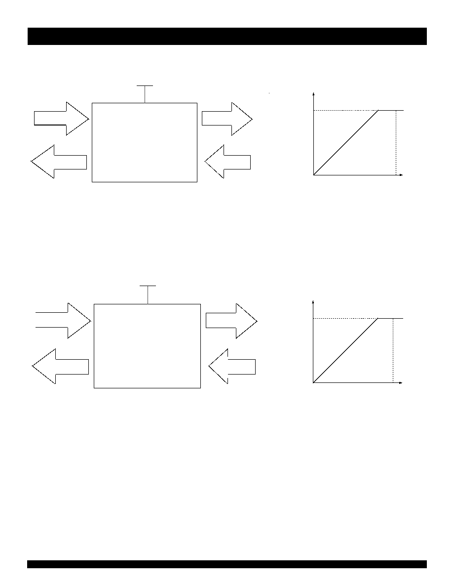
QS34XV245
2.5V
2.5V
3.3V
2.5V
3.3V
Q S34XV245
1.8V
1.8V
2.5V
1.8V
2.5V
V
IN
2.5V
V
O UT
3.3V
Supply
0V
3.3V
Swi
t
ch
O
u
t
put
Switch Input
V
IN
1.8V
2.5V
Supply
0V
2.5V
V
O U T
Swi
t
c
h O
u
t
put
Switch Input
2.5V TO 1.8V VOLTAGE TRANSLATION
3.3V TO 2.5V VOLTAGE TRANSLATION
Figure. 5
Figure. 8
Figure. 7
Figure. 6

7
INDUSTRIAL TEMPERATURE RANGE
IDTQS34XV245
3.3V HIGH SPEED 32-BIT MULTIWIDTH BUS SWITCH
ORDERING INFORMATION
ID TQS
X X X XX
X X
X
P ackage
P rocess
D evice Type
B lank
34XV 245
Industrial (-40∞C to +85∞C )
3.3V H igh S peed 32-B it M ultiw idth B us S w itch
Q 3
80-P in M illipaQ
CORPORATE HEADQUARTERS
for SALES:
2975 Stender Way
800-345-7015 or 408-727-6116
Santa Clara, CA 95054
fax: 408-492-8674
www.idt.com*
*To search for sales office near you, please click the sales button found on our home page or dial the 800# above and press 2.
The IDT logo, QuickSwitch, and SynchroSwitch are registered trademarks of Integrated Device Technology, Inc.