
1
IDTQS34XST257
HIGH-SPEED CMOS SYNCHROSWITCH 32:16 MUX/DEMUX
INDUSTRIAL TEMPERATURE RANGE
NOVEMBER 1999
1999 Integrated Device Technology, Inc.
DSC-5532/-
c
IDTQS34XST257
INDUSTRIAL TEMPERATURE RANGE
QUICKSWITCH
Æ
PRODUCTS
HIGH-SPEED CMOS
SYNCHROSWITCHTM 32:16 MUX/
DEMUX WITH ACTIVE TERMINATORS
DESCRIPTION:
The QS34XST257 is a high-speed CMOS quad 32:16 multiplexer/
demultiplexer with active terminators (bus-hold circuits) on the demux side.
It is organized as four independent quad 2:1 mux/demux blocks. Port
selection and connection, controlled by SEL signals, can be either asyn-
chronous or synchronous. In the synchronous mode, the A or B port to Y
port connection is updated on the rising edge of the input clock CLK. Once
the port-to-port connection is made, data flow can be bi-directional with a
typical 250ps propagation delay through the switch. Clock Enable,
overriding Asynchronous Enable, and Asynchronous Select controls
provide additional design flexibility.
The bus-hold circuits latch the last data driven on the demux side,
providing infinite hold time and glitch-free signal transitions. Synchronous
controls and bus-hold ease timing constraints in many high speed data mux/
demux applications, such as bank interleaving. The QS34XST257 is
available in the space-saving, 80-pin dual-in-line MillipaQ package.
The QS34XST257 is characterized for operation at -40∞C to +85∞C.
SELn
CLKn
CLKENn
OEn
SYNC n
Yn
0
Yn
1
Yn
2
Yn
3
An
0
Bn
0
An
1
An
2
An
3
Bn
1
Bn
2
Bn
3
T
T
T
T
T
T
T
T
T
=
R
CO NTR OL
LOGIC
NOTE: One of four blocks shown.
FUNCTIONAL BLOCK DIAGRAM
FEATURES:
-
Enhanced N channel FET with no inherent diode to Vcc
-
Bidirectional signal flow
-
Flow-through pinout
-
Zero propagation delay, zero ground bounce
-
16 banks of 2:1 Mux/Demux
-
Port select synchronous to the clock
-
Clock enable and Asynchronous enable
-
"Bus-hold" terminators on the Demux side
-
Undershoot clamp diodes on all switch and control pins
-
Asynchronous SEL option
-
Break-before-make feature
-
Available in 80-pin MillipaQ (Q3)
-
Bus-hold eliminates floating bus lines and reduces static power
consumption
APPLICATIONS:
-
Memory Interleaving
2
INDUSTRIAL TEMPERATURE RANGE
IDTQS34XST257
HIGH-SPEED CMOS SYNCHROSWITCH 32:16 MUX/DEMUX
NC
A
00
A
01
A
02
A
03
B
00
B
01
B
02
B
03
G ND
NC
A
10
A
11
A
12
A
13
B
10
B
11
B
12
B
13
NC
A
20
A
21
A
22
A
23
B
20
B
21
B
22
B
23
G ND
NC
A
30
A
31
A
32
A
33
B
30
B
31
B
32
B
33
G ND
G ND
2
3
4
5
6
7
8
73
74
75
76
77
78
79
80
1
55
54
53
52
51
50
49
48
47
46
45
44
43
42
41
56
9
10
11
12
13
14
15
16
17
18
19
20
21
22
23
24
39
38
37
36
35
34
33
32
31
30
29
28
27
26
40
25
58
59
60
61
62
63
64
65
66
67
68
69
70
71
57
72
Vcc
O E
0
SEL
0
Y
00
Y
01
Y
02
Y
03
CLKEN
0
CLK
0
SYN C
0
Vcc
O E
1
SEL
1
Y
10
Y
11
Y
12
Y
13
CLKEN
1
CLK
1
SYN C
1
Vcc
O E
2
SEL
2
Y
20
Y
21
Y
22
Y
23
CLKEN
2
CLK
2
SYN C
2
Vcc
O E
3
SEL
3
Y
30
Y
31
Y
32
Y
33
CLKEN
3
CLK
3
SYN C
3
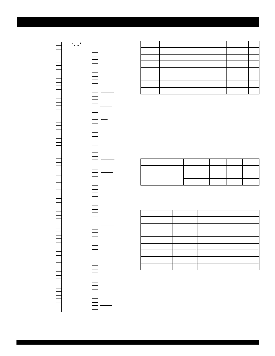
PIN CONFIGURATION
ABSOLUTE MAXIMUM RATINGS
(1)
Symbol
Description
Max.
Unit
V
TERM(2)
Supply Voltage to Ground
≠ 0.5 to +7
V
V
TERM(3)
DC Switch Voltage V
S
≠ 0.5 to +7
V
V
TERM(3)
DC Input Voltage V
IN
≠ 0.5 to +7
V
V
AC
AC Input Voltage (pulse width
20ns)
-3
V
I
OUT
DC Output Current
120
mA
P
MAX
Maximum Power Dissipation (T
A
= 85
∞
C)
1.16
W
T
STG
Storage Temperature
≠ 65 to +150
∞C
NOTES:
1. Stresses greater than those listed under ABSOLUTE MAXIMUM
RATINGS may cause permanent damage to the device. This is a
stress rating only and functional operation of the device at these or
any other conditions above those indicated in the operational sections
of this specification is not implied. Exposure to absolute maximum
rating conditions for extended periods may affect reliability.
2. Vcc Terminals.
3. All terminals except Vcc.
CAPACITANCE
(T
A
= +25
O
C, f = 1.0MHz, V
IN
= 0V, V
OUT
= 0V)
Pins
Typ.
Max.
(1)
Unit
Control Inputs
4
5
pF
Quickswitch Channels
Demux
5
7
pF
(Switch OFF)
Mux
7
9
pF
NOTE:
1. This parameter is guaranteed at characterization but not tested.
PIN DESCRIPTION
Pin Names
I/O
Description
An
0
- An
3
I/O
Demux Port A
Bn
0
- Bn
3
I/O
Demux Port B
Yn
0
- Yn
3
I/O
Mux Port Y
SELn
I
Select Input
CLKn
I
Clock
CLKENn
I
Clock Enable
OEn
I
Output Enable
SYNCn
I
Synchronous Selection Enable
MILLIPAQ
TOP VIEW
3
IDTQS34XST257
HIGH-SPEED CMOS SYNCHROSWITCH 32:16 MUX/DEMUX
INDUSTRIAL TEMPERATURE RANGE
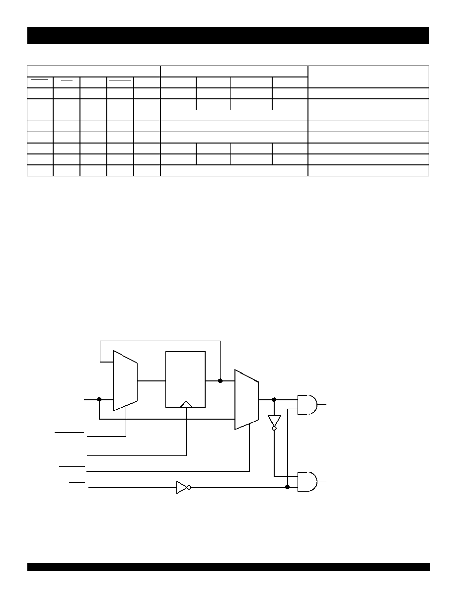
FUNCTION TABLE
(1)
Control Inputs
Port Status
Function
SYNC
OEn
CLKn
CLKENn
SELn
Yn
0
Yn
1
Yn
2
Yn
3
L
L
L
L
An
0
An
1
An
2
An
3
Select Port A
L
L
L
H
Bn
0
Bn
1
Bn
2
Bn
3
Select Port B
L
H
L
X
No change in Mux connection
Hold Previous Data
(2)
(Switch OFF)
L
L
H
X
No change in Mux connection
Hold Previous Mux connection
(3)
(Switch ON)
L
H
H
X
No change in Mux connection
Hold Previous Data
(4)
(Switch OFF)
H
L
X
X
L
An
0
An
1
An
2
An
3
Select Port A
H
L
X
X
H
Bn
0
Bn
1
Bn
2
Bn
3
Select Port B
H
H
X
X
X
No change in Mux connection
Hold Previous Data (Switch OFF)
NOTES:
1. H = HIGH Voltage Level
L = LOW Voltage Level
X = Don't Care
= Low-to-High Transition
2. Mux switches are turned off and the terminators (last value latches) hold the previous data state. The port connection can be changed by the SEL
input.
3. The contents of the "Mux select register" are unchanged and the previous Mux connection is unchanged. The output (Mux port) data state will
depend on the present data state of the input (Demux port).
4. The contents of the "Mux select register" are unchanged and the last value latches hold the previous data state.
1
2:1
M U X
0
SE Ln
C LK EN n
C LK n
SYN C n
O En
0
2:1
M U X
1
D
Q
To Port B Sw itches
To Port A Sw itches
CONTROL LOGIC
(1)
NOTE:
1. One of four blocks.

4
INDUSTRIAL TEMPERATURE RANGE
IDTQS34XST257
HIGH-SPEED CMOS SYNCHROSWITCH 32:16 MUX/DEMUX
0.0
0.5
1.0
1.5
2.0
2.5
3.0
3.5
0
2
4
6
8
10
12
14
16
TYPICAL ON RESISTANCE vs V
IN
AT V
CC
= 5V
R
ON
(ohms)
V
IN
(Volts)
DC ELECTRICAL CHARACTERISTICS OVER OPERATING RANGE
Following Conditions Apply Unless Otherwise Specified:
Industrial: T
A
= -40∞C to +85∞C, V
CC
= 5.0V ± 10%
Symbol
Parameter
Test Conditions
Min.
Typ.
(1)
Max.
Unit
V
IH
Input HIGH Voltage
Guaranteed Logic HIGH for Control Pins
2
--
--
V
V
IL
Input LOW Voltage
Guaranteed Logic LOW for Control Pins
--
--
0.8
V
I
IN
Input Leakage Current (Control Inputs)
0V
V
IN
Vcc
--
0.01
±1
µ
A
R
ON
Switch On Resistance
(2)
Vcc = Min., V
IN
= 0V
,
I
ON
= 30mA
--
7
9
Vcc = Min., V
IN
= 2.4V
,
I
ON
= 15mA
--
10
13
I
BHL
Input Hold Current
(3,4)
Vcc = Min.
V
IN
= 0.8V
60
--
--
µ
A
I
BHH
(A or B port)
Switch OFF
V
IN
= 2V
≠
60
--
--
I
BH
Input Current
(6)
Vcc = Max.
V
IN
= 0V or Vcc
--
--
±20
µ
A
A and B port
0.8 < V
IN
< 2V
--
--
±500
(5)
NOTES:
1. Typical values are at V
CC
= 5.0V, T
A
= 25∞C.
2. Measured by voltage drop between A/B and Y pin at indicated current through the switch.
3. I
BHL
is the minimum sustaining "sink" current at the input for V
IN
= 0.8V. This parameter signifies the latching capability of the bus-hold circuit in
logic LOW state.
4. I
BHH
is the minimum sustaining "source" current at the input for V
IN
= 2V. This parameter signifies the latching capability of the bus-hold circuit in
logic HIGH state.
5. An external driver must provide at least I
BH
during transition to guarantee that the bus-hold input will change states.
6. I
BH
is the magnitude of the input current specified under two conditions:
a)
Input voltage at GND or Vcc. This indicates the input current under steady-state condition.
b)
Input voltage between 0.8V and 2V (TTL input threshold range). This indicates the maximum input current during transient condition. The
driver connected to the input must overcome this current requirement in order to switch the logic state of the bus-hold circuit.

5
IDTQS34XST257
HIGH-SPEED CMOS SYNCHROSWITCH 32:16 MUX/DEMUX
INDUSTRIAL TEMPERATURE RANGE
POWER SUPPLY CHARACTERISTICS
Symbol
Parameter
Test Conditions
(1)
Max.
Unit
I
CCQ
Quiescent Power Supply Current
V
CC
= Max., V
CTRL
= GND or Vcc, f = 0
12
mA
I
CC
Power Supply Current per Control Input HIGH
(2)
V
CC
= Max., V
IN
= 3.4V, f = 0
1.5
mA
I
CCD
Dynamic Power Supply Current per MHz
(3)
V
CC
= Max., A/B and Y pins open
Control Input Toggling at 50% Duty Cycle
0.25
mA/MHz
NOTES:
1. For conditions shown as Min. or Max., use the appropriate values specified under DC Electrical Characteristics.
2. Per TLL driven control inputs. A/B and Y pins do not contribute to
Icc
.
3. This current applies to the control inputs only and represents the current required to switch internal capacitance at the specified frequency. The A/B
and Y inputs generate no significant AC or DC currents as they transition. This parameter is guaranteed but not production tested.
SWITCHING CHARACTERISTICS OVER OPERATING RANGE
T
A
= -40∞C to +85∞C, V
CC
= 5.0V ± 10%
C
LOAD
= 50pF, R
LOAD
= 500
unless otherwise noted.
Symbol
Parameter
Min.
Typ.
Max.
Unit
t
PLH
t
PHL
Data Propagation Delay
(1,2)
A/B to Y, Y to A/B
--
0.25
--
ns
t
SEC
Clock Enable to Clock Setup Time
3
--
--
ns
t
HEC
Clock Enable to Clock Hold Time
0
--
--
ns
t
CSO
Clock to A, B Switch Turn-On Delay
(3)
0.5
--
7
ns
t
ASO
Asynchronous Select to A, B Switch Turn-On Delay
(3)
0.5
--
7
ns
t
W
Clock Pulse Width HIGH
3
--
--
ns
t
SCS
Clock to SEL Setup Time
3
--
--
ns
t
HCS
Clock to SEL Hold Time
0
--
--
ns
t
PZL
t
PZH
Asynchronous Enable to Switch Turn-On Delay
(3)
1.5
--
5.2
ns
t
PLZ
t
PHZ
Asynchronous Enable to Switch Turn-Off Delay
(1,3)
1.5
--
4.8
ns
NOTES:
1. This parameter is guaranteed but not tested.
2. The bus switch contributes no propagation delay other than the RC delay of the ON resistance of the switch and the load capacitance. The time
constraint for the switch alone is of the order of 0.25ns for C
L
= 50pF. Since this time constant is much smaller than the rise and fall times of typical
driving signals, it adds very little propagation delay to the system. Propagation delay of the bus switch, when used in a system, is determined by the
driving circuit on the driving side of the switch and its interaction with the load on the driven side.
3. Minimums guaranteed but not tested.
6
INDUSTRIAL TEMPERATURE RANGE
IDTQS34XST257
HIGH-SPEED CMOS SYNCHROSWITCH 32:16 MUX/DEMUX
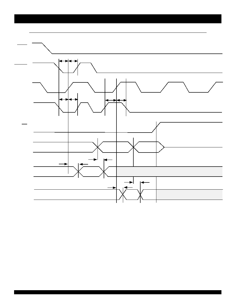
TIMING WAVEFORMS - SYNCHRONOUS MODE, DEMUX FUNCTION
SY NC
CLK EN
CLK
SE L
O E
Port Y
Port A
Port B
HO LD PR EVIO US DAT A, DATA 1
HO LD PR EVIO US DAT A, DATA 2
DAT A 1
DAT A 2
IN V ALID D ATA
DAT A
1
DAT A 0
IN V ALID D ATA
t
SEC
t
H EC
t
SC S
t
H CS
t
SC S
t
H CS
t
PLH ,
t
PH L
t
C SO
t
PLH ,
t
PH L
t
C SO
DAT A 1
DAT A 2
DAT A 0
7
IDTQS34XST257
HIGH-SPEED CMOS SYNCHROSWITCH 32:16 MUX/DEMUX
INDUSTRIAL TEMPERATURE RANGE
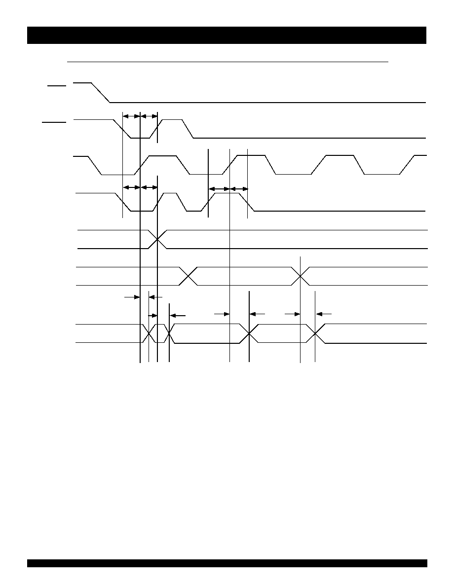
TIMING WAVEFORMS - SYNCHRONOUS MODE, MUX FUNCTION
SY NC
CLKEN
CLK
SEL0, SE L1
Port A
Port D
Port Y
D AT A1
DAT A2
INVALID D ATA
DATA3
DAT A4
t
SE C
t
H EC
t
SC S
t
H CS
t
SC S
t
H CS
DAT A1
DAT A2
INV ALID D ATA
DAT A3
DAT A4
t
C SO
t
PLH ,
t
PH L
t
C SO
t
PLH ,
t
PH L

8
INDUSTRIAL TEMPERATURE RANGE
IDTQS34XST257
HIGH-SPEED CMOS SYNCHROSWITCH 32:16 MUX/DEMUX
TIMING WAVEFORMS - ASYNCHRONOUS MODE, MUX FUNCTION
S Y N C
S E L
O E
P o r t A
P o r t B
P o r t Y
I N V A L I D
D A T A
D A T A 1
D A T A 2
I N V A L I D D A T A
D A T A 3
I N V A L I D D A T A
D A T A 1
D A T A 2
D A T A 3
D A T A 3
t
P L H ,
t
P H L
t
P L H ,
t
P H L
t
A S O
t
P L Z ,
t
P H Z
t
P Z L ,
t
P Z H

9
IDTQS34XST257
HIGH-SPEED CMOS SYNCHROSWITCH 32:16 MUX/DEMUX
INDUSTRIAL TEMPERATURE RANGE
ACTIVE TERMINATOR OR BUS-HOLD CIRCUIT
The Active Terminator circuit, also known as the bus-hold circuit, is configured as a "weak latch" with positive feedback. When connected to a
TTL or CMOS input port, the bus-hold circuit holds the last logic state at the input when the input is "disconnected" from the driver. When the output
of a device connected to such an input attempts a logic level transition, it will overdrive the bus-hold circuit. The primary benefit of a bus-hold circuit
is that it prevents CMOS inputs from floating, a situation which should be avoided to prevent spurious switching of inputs and unnecessary power
dissipation. Bus-hold is a better solution than the traditional approach of using resistive termination to Vcc or GND to prevent bus floating, because
the bus-hold circuit does not consume any static power.
I
B H
+500
Sinking
C urrent
( + )
I
BHL
I
B H
I
BH H
+60
+20
≠ 60
≠ 20
+60 I
B HL
0.8V
2V
V
IH
≠ 60 I
B HL
V
IL
Sourcing
C urrent
( ≠ )
I
B H
≠ 500
Vcc
+20 I
BH
≠ 20 I
BH
Voltage
V
T
V-I CHARACTERISTICS OF BUS-HOLD CIRCUIT
V
T
Threshold Voltage
1.5V
V
IL
.8 V
IH
2V
This figure shows the input V-I characteristics of a typical bus-hold implementation. The input characteristics resemble a resistor. As the input
voltage is increased from 0 volts, the input "sink" current increases linearly. When the TTL threshold of the circuit is reached (typically 1.5 volts), the
latch changes the logic state due to positive feedback and the direction of the current is reversed. As the input voltage is further increased towards
Vcc, the input "source" current begins to decrease, reaching the lowest level at V
IN
= Vcc.
10
INDUSTRIAL TEMPERATURE RANGE
IDTQS34XST257
HIGH-SPEED CMOS SYNCHROSWITCH 32:16 MUX/DEMUX
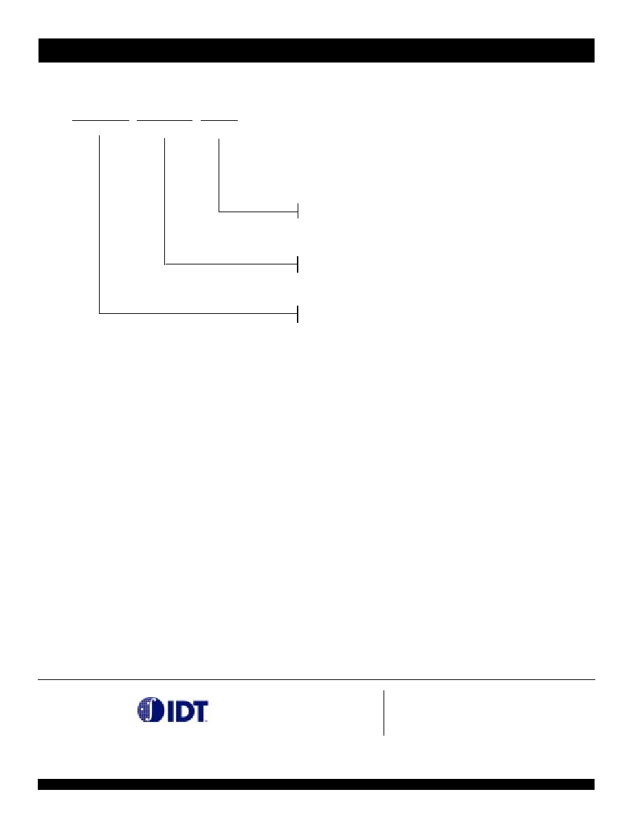
IDTQS
XXXXX
XX
Package
Device Type
Blank
Extended Com m ercial (-40∞C to +85∞C )
150 m il M illipaQ
Q3
34XST257
High Speed CM OS SynchroSwitch 32:16
M ux/Dem ux with Active Term inators
X
Process
ORDERING INFORMATION
CORPORATE HEADQUARTERS
for SALES:
2975 Stender Way
800-345-7015 or 408-727-6116
Santa Clara, CA 95054
fax: 408-492-8674
www.idt.com*
*To search for sales office near you, please click the sales button found on our home page or dial the 800# above and press 2.
The IDT logo, QuickSwitch, and SynchroSwitch are registered trademarks of Integrated Device Technology, Inc.