Aug-06-2001
1
BAS19...BAS21
1
2
3
VPS05161
Silicon Switching Diodes
High-speed, high-voltage switching applications
1
3
EHA07002
Type
Marking
Pin Configuration
Package
BAS19
BAS20
BAS21
JPs
JRs
JSs
1 = A
1 = A
1 = A
2 = n.c.
2 = n.c.
2 = n.c.
3 = C
3 = C
3 = C
SOT23
SOT23
SOT23
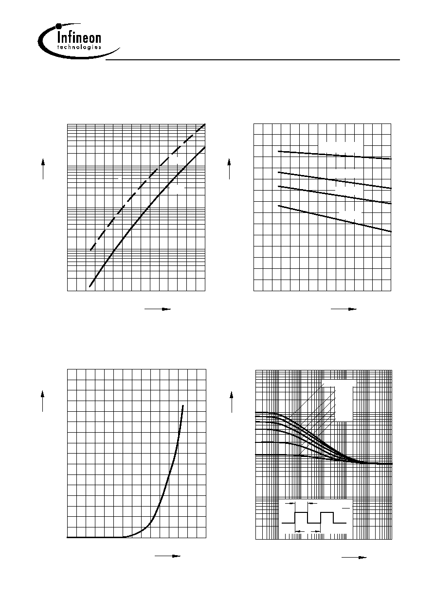
Maximum Ratings
Parameter
Symbol
Value
Unit
Diode reverse voltage
BAS19
BAS20
BAS21
V
R
100
150
200
V
Peak reverse voltage-
BAS19
BAS20
BAS21
V
RM
120
200
250
Forward current
I
F
250
mA
Peak forward current
I
FM
625
Total power dissipation
T
S
= 70 �C
P
tot
350
mW
Junction temperature
T
j
150
�C
Storage temperature
T
stg
-65 ... 150
Thermal Resistance
Parameter
Symbol
Value
Unit
Junction - soldering point
1)
R
thJS
230
K/W
1
For calculation of R
thJA
please refer to Application Note Thermal Resistance
Aug-06-2001
2
BAS19...BAS21
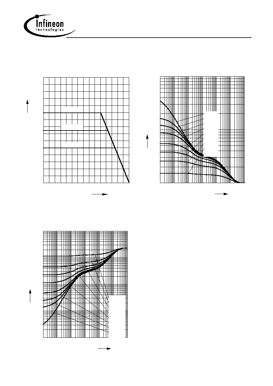
Electrical Characteristics at T
A
= 25�C, unless otherwise specified
Parameter
Symbol
Values
Unit
min.
typ.
max.
DC Characteristics
Breakdown voltage
I
(BR)
= 100 �A, BAS19
I
(BR)
= 100 �A, BAS20
I
(BR)
= 100 �A, BAS21
V
(BR)
120
200
250
-
-
-
-
-
-
V
Reverse current
V
R
= V
Rmax
V
R
= V
Rmax
, T
A
= 150 �C
I
R
-
-
-
-
0.1
100
�A
Forward voltage
I
F
= 100 mA
I
F
= 200 mA
V
F
-
-
-
-
1
1.25
V
AC Characteristics
Diode capacitance-
V
R
= 0 V, f = 1 MHz
C
T
-
-
5
pF
Reverse recovery time
I
F
= 30 mA, I
R
= 30 mA, measured at I
R
= 3 mA,
R
L
= 100
t
rr
-
-
50
ns
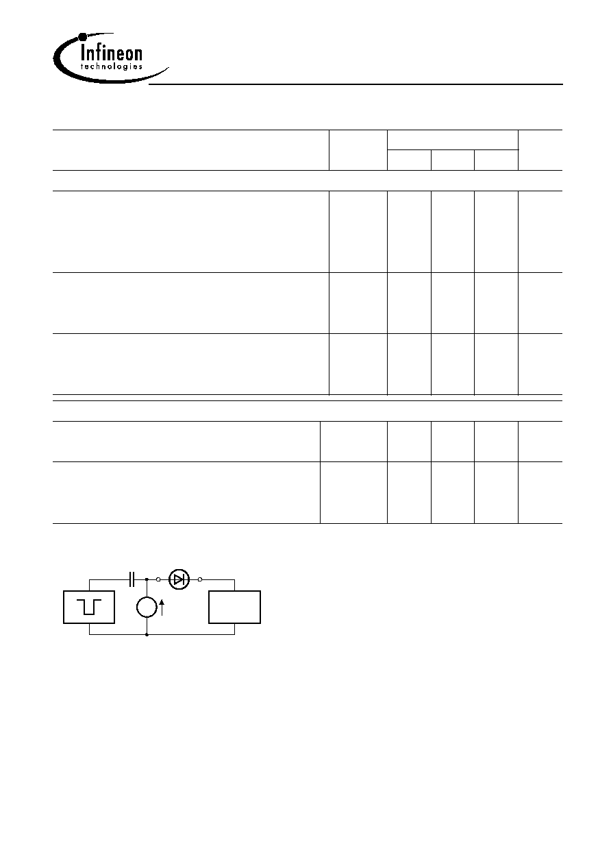
Test circuit for reverse recovery time
EHN00018
Oscillograph
F
D.U.T.
Pulse generator: t
p
= 1
s, D = 0.05,
t
r
= 0.6 ns, R
i
= 50
Oscillograph: R = 50
, t
r
= 0.35 ns, C
1 pF