 | –≠–ª–µ–∫—Ç—Ä–æ–Ω–Ω—ã–π –∫–æ–º–ø–æ–Ω–µ–Ω—Ç: BFP620F | –°–∫–∞—á–∞—Ç—å:  PDF PDF  ZIP ZIP |
BFP620F
Apr-21-2004
1
NPN Silicon Germanium RF Transistor*
∑
High gain low noise RF transistor
∑
Small package 1.4 x 0.8 x 0.59 mm
∑
Outstanding noise figure F = 0.7 dB at 1.8 GHz
Outstanding noise figure F = 1.3 dB at 6 GHz
∑
Maximum stable gain
G
ms
= 21 dB at 1.8 GHz
G
ma
= 10 dB at 6 GHz
∑
Gold metallization for extra high reliability
*Short-term description
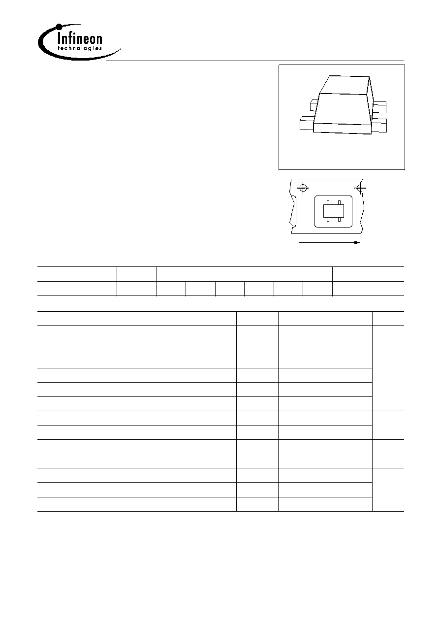
TSFP-4
1
2
4
3
XYs
1
3
4
2
Direction of Unreeling
Top View
XYs
ESD
: Electrostatic discharge sensitive device, observe handling precaution!
Type
Marking
Pin Configuration
Package
BFP620F
R2s
1=B
2=E
3=C
4=E
-
-
TSFP-4
Maximum Ratings
Parameter
Symbol
Value
Unit
Collector-emitter voltage
T
A
> 0 ∞C
T
A
0 ∞C
V
CEO
2.3
2.1
V
Collector-emitter voltage
V
CES
7.5
Collector-base voltage
V
CBO
7.5
Emitter-base voltage
V
EBO
1.2
Collector current
I
C
80
mA
Base current
I
B
3
Total power dissipation
1)
T
S
96∞C
P
tot
185
mW
Junction temperature
T
j
150
∞C
Ambient temperature
T
A
-65 ... 150
Storage temperature
T
stg
-65 ... 150
1TS is measured on the collector lead at the soldering point to the pcb

BFP620F
Apr-21-2004
2
Thermal Resistance
Parameter
Symbol
Value
Unit
Junction - soldering point
1)
R
thJS
290
K/W
Electrical Characteristics at T
A
= 25∞C, unless otherwise specified
Parameter
Symbol
Values
Unit
min.
typ.
max.
DC Characteristics
Collector-emitter breakdown voltage
I
C
= 1 mA, I
B
= 0
V
(BR)CEO
2.3
2.8
-
V
Collector-emitter cutoff current
V
CE
= 7.5 V, V
BE
= 0
I
CES
-
-
10
µA
Collector-base cutoff current
V
CB
= 5 V, I
E
= 0
I
CBO
-
-
100
nA
Emitter-base cutoff current
V
EB
= 0.5 V, I
C
= 0
I
EBO
-
-
3
µA
DC current gain
I
C
= 50 mA, V
CE
= 1.5 V, pulse measured
h
FE
110
180
270
-
1For calculation of
R
thJA
please refer to Application Note Thermal Resistance

BFP620F
Apr-21-2004
3
Electrical Characteristics at T
A
= 25∞C, unless otherwise specified
Parameter
Symbol
Values
Unit
min.
typ.
max.
AC Characteristics (verified by random sampling)
Transition frequency
I
C
= 50 mA, V
CE
= 1.5 V, f = 1 GHz
f
T
-
65
-
GHz
Collector-base capacitance
V
CB
= 2 V, f = 1 MHz
C
cb
-
0.12
0.2
pF
Collector emitter capacitance
V
CE
= 2 V, f = 1 MHz
C
ce
-
0.2
-
Emitter-base capacitance
V
EB
= 0.5 V, f = 1 MHz
C
eb
-
0.45
-
Noise figure
I
C
= 5 mA, V
CE
= 1.5 V, f = 1.8 GHz, Z
S
= Z
Sopt
I
C
= 5 mA, V
CE
= 1.5 V, f = 6 GHz, Z
S
= Z
Sopt
F
-
-
0.7
1.3
-
-
dB
Power gain, maximum stable
1)
I
C
= 50 mA, V
CE
= 1.5 V, Z
S
= Z
Sopt
,
Z
L
= Z
Lopt
, f = 1.8 GHz
G
ms
-
21
-
dB
Power gain, maximum available
1)
I
C
= 50 mA, V
CE
= 1.5 V, Z
S
= Z
Sopt
,
Z
L
= Z
Lopt
, f = 6 GHz
G
ma
-
10
-
dB
Transducer gain
I
C
= 50 mA, V
CE
= 1.5 V, Z
S
= Z
L
= 50
,
f = 1.8 GHz
I
C
= 50 mA, V
CE
= 1.5 V, Z
S
= Z
L
= 50
,
f = 6 GHz
|S
21e
|
2
-
-
19.5
9.5
-
-
dB
Third order intercept point at output
2)
V
CE
= 2 V, I
C
= 50 mA, f = 1.8 GHz,
Z
S
= Z
L
= 50
IP
3
-
25
-
dBm
1dB Compression point at output
I
C
= 50 mA, V
CE
= 2 V, Z
S
= Z
L
= 50
,
f = 1.8 GHz
P
-1dB
-
14
-
1
G
ma
= |
S
21e
/
S
12e
| (k-(k≤-1)
1/2
),
G
ms
= |
S
21e
/
S
12e
|
2IP3 value depends on termination of all intermodulation frequency components.
Termination used for this measurement is 50
from 0.1 MHz to 6 GHz
BFP620F
Apr-21-2004
4
SPICE Parameter (Gummel-Poon Model, Berkley-SPICE 2G.6 Syntax):
Transitor Chip Data:
IS =
0.22
fA
VAF =
1000
V
NE =
2
-
VAR =
2
V
NC =
2
-
RBM =
2.707
CJE =
250.7
fF
TF =
1.43
ps
ITF =
2.4
A
VJC =
0.6
V
TR =
0.2
ns
MJS =
0.5
-
XTI =
3
-
AF =
2
-
TITF1
-0.0065
-
NF =
1.025
-
ISE =
21
fA
NR =
1
-
ISC =
18
pA
IRB =
1.522
mA
RC =
2.364
MJE =
0.3
-
VTF =
1.5
V
CJC =
124.9
fF
XCJC =
1
-
VJS =
0.52
V
EG =
1.078
eV
TNOM
298
K
BF =
425
-
IKF =
0.25
A
BR =
50
-
IKR =
10
mA
RB =
3.129
RE =
0.6
-
VJE =
0.75
V
XTF =
10
-
PTF =
0
deg
MJC =
0.5
-
CJS =
128.1
fF
NK =
-1.42
-
FC =
0.8
KF =
7.291E-11
TITF2
1.0E-5
All parameters are ready to use, no scalling is necessary.
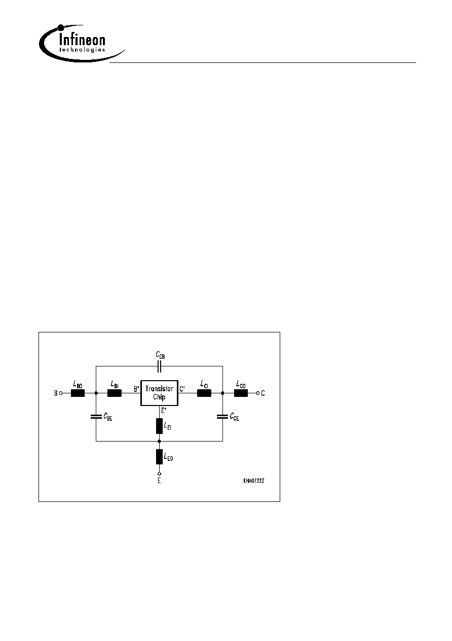
Package Equivalent Circuit:
L
B0
=
0.22
nH
L
E0
=
0.28
nH
L
C0
=
0.22
nH
K
B0-E0
= 0.1
-
K
B0-C0
= 0.01
-
K
E0-C0
= 0.11
-
C
BE
=
34
fF
C
BC
=
2
fF
C
CE
=
33
fF
L
BI
=
0.42
nH
R
LBI
=
0.15
L
EI
=
0.26
nH
R
LEI
=
0.11
L
CI
=
0.35
nH
R
LI
=
0.13
K
BI-EI
=
-0.05
-
K
BI-CI
=
-0.08
-
K
EI-CI
=
0.2
-
To avoid high complexity of the package equivalent circuit,
both emitter leads of
TSFP-4
are combined in one electrical
connection.
R
LxI
are series resistors for the inductances
L
xI
and
K
xa-yb
are the coupling coefficients between the
inductances
L
xa
and
L
yb
.
Valid up to 6GHz

BFP620F
Apr-21-2004
5
Total power dissipation P
tot
=
(T
S
)
0
15
30
45
60
75
90 105 120 ∞C
150
T
S
0
20
40
60
80
100
120
140
160
mW
200
P
tot
Permissible Pulse Load R
thJS
=
(t
p
)
10
-7
10
-6
10
-5
10
-4
10
-3
10
-2
10
0
s
t
p
1
10
2
10
3
10
K/W
R
thJS
0.5
0.2
0.1
0.05
0.02
0.01
0.005
D = 0
Permissible Pulse Load
P
totmax
/P
totDC
=
(t
p
)
10
-7
10
-6
10
-5
10
-4
10
-3
10
-2
10
0
s
t
p
0
10
1
10
P
totmax
/
P
totDC
D = 0
0.005
0.01
0.02
0.05
0.1
0.2
0.5
Collector-base capacitance C
cb
=
(V
CB
)
f = 1MHz
0
1
2
3
4
5
6
V
8
V
CB
0
0.05
0.1
0.15
0.2
0.25
0.3
pF
0.4
C
CB