 | –≠–Ľ–Ķ–ļ—ā—Ä–ĺ–Ĺ–Ĺ—č–Ļ –ļ–ĺ–ľ–Ņ–ĺ–Ĺ–Ķ–Ĺ—ā: BFP740F | –°–ļ–į—á–į—ā—Ć:  PDF PDF  ZIP ZIP |

2005-11-08
BFP740F
1
NPN Silicon Germanium RF Transistor
∑
High gain ultra low noise RF transistor
∑
Provides outstanding performance for
a wide range of wireless applications
up to 10 GHz and more
∑
Ideal for CDMA and WLAN applications
∑
Outstanding noise figure F = 0.5 dB at 1.8 GHz
Outstanding noise figure F = 0.75 dB at 6 GHz
∑
High maximum stable gain
G
ms
= 27.5 dB at 1.8 GHz
∑
Gold metallization for extra high reliability
∑
150 GHz f
T
-Silicon Germanium technology
1
2
4
3
1
3
4
2
Direction of Unreeling
Top View
XYs
ESD
(Electrostatic discharge) sensitive device, observe handling precaution!
Type
Marking
Pin Configuration
Package
BFP740F
R7s
1=B
2=E
3=C
4=E
-
-
TSFP-4
Maximum Ratings
Parameter
Symbol
Value
Unit
Collector-emitter voltage
T
A
> 0įC
T
A
0įC
V
CEO
4
3.5
V
Collector-emitter voltage
V
CES
13
Collector-base voltage
V
CBO
13
Emitter-base voltage
V
EBO
1.2
Collector current
I
C
30
mA
Base current
I
B
3
Total power dissipation
1)
T
S
90įC
P
tot
160
mW
Junction temperature
T
j
150
įC
Ambient temperature
T
A
-65 ... 150
Storage temperature
T
stg
-65 ... 150
1TS is measured on the collector lead at the soldering point to the pcb
2005-11-08
BFP740F
2
Thermal Resistance
Parameter
Symbol
Value
Unit
Junction - soldering point
1)
R
thJS
370
K/W
Electrical Characteristics at T
A
= 25įC, unless otherwise specified
Parameter
Symbol
Values
Unit
min.
typ.
max.
DC Characteristics
Collector-emitter breakdown voltage
I
C
= 1 mA, I
B
= 0
V
(BR)CEO
4
4.7
-
V
Collector-emitter cutoff current
V
CE
= 13 V, V
BE
= 0
I
CES
-
-
30
ĶA
Collector-base cutoff current
V
CB
= 5 V, I
E
= 0
I
CBO
-
-
100
nA
Emitter-base cutoff current
V
EB
= 0.5 V, I
C
= 0
I
EBO
-
-
3
ĶA
DC current gain
I
C
= 25 mA, V
CE
= 3 V, pulse measured
h
FE
160
250
400
-
1For calculation of
R
thJA
please refer to Application Note Thermal Resistance
2005-11-08
BFP740F
3
Electrical Characteristics at T
A
= 25įC, unless otherwise specified
Parameter
Symbol
Values
Unit
min.
typ.
max.
AC Characteristics (verified by random sampling)
Transition frequency
I
C
= 25 mA, V
CE
= 3 V, f = 1 GHz
f
T
-
42
-
GHz
Collector-base capacitance
V
CB
= 3 V, f = 1 MHz, V
BE
= 0 ,
emitter grounded
C
cb
-
0.08
0.14 pF
Collector emitter capacitance
V
CE
= 3 V, f = 1 MHz, V
BE
= 0 ,
base grounded
C
ce
-
0.2
-
Emitter-base capacitance
V
EB
= 0.5 V, f = 1 MHz, V
CB
= 0 ,
collector grounded
C
eb
-
0.44
-
Noise figure
I
C
= 8 mA, V
CE
= 3 V, f = 1.8 GHz, Z
S
= Z
Sopt
I
C
= 8 mA, V
CE
= 3 V, f = 6 GHz, Z
S
= Z
Sopt
F
-
-
0.5
0.75
-
-
dB
Power gain, maximum stable
1)
I
C
= 25 mA, V
CE
= 3 V, Z
S
= Z
Sopt
,
Z
L
= Z
Lopt
, f = 1.8 GHz
G
ms
-
27.5
-
dB
Power gain, maximum available
1)
I
C
= 25 mA, V
CE
= 3 V, Z
S
= Z
Sopt
,
Z
L
= Z
Lopt
, f = 6 GHz
G
ma
-
19
-
dB
Transducer gain
I
C
= 25 mA, V
CE
= 3 V, Z
S
= Z
L
= 50
,
f = 1.8 GHz
f = 6 GHz
|S
21e
|
2
-
-
25
15
-
-
dB
Third order intercept point at output
2)
V
CE
= 3 V, I
C
= 25 mA, Z
S
=Z
L
=50
,
f
=
1
.
8
GHz
IP
3
-
25
-
dBm
1dB Compression point at output
I
C
= 25 mA, V
CE
= 3 V, Z
S
=Z
L
=50
,
f
=
1
.
8
GHz
P
-1dB
-
11
-
1
G
ma
= |
S
21e
/
S
12e
| (k-(k≤-1)
1/2
),
G
ms
= |
S
21e
/
S
12e
|
2IP3 value depends on termination of all intermodulation frequency components.
Termination used for this measurement is 50
from 0.1 MHz to 6 GHz
2005-11-08
BFP740F
4
SPICE Parameter (Gummel-Poon Model, Berkley-SPICE 2G.6 Syntax):
Transitor Chip Data:
IS =
384.4
aA
VAF =
400
V
NE =
1.586
-
VAR =
1.28
V
NC =
1.5
-
RBM =
1.69
CJE =
220
fF
TF =
2.1
ps
ITF =
290
mA
VJC =
550
mV
TR =
13
ps
MJS =
180
m
XTI =
910
m
AF =
1
-
NF =
1.018
-
ISE =
4.296
fA
NR =
1
-
ISC =
3.85
fA
IRB =
10
A
RC =
6.88
MJE =
70
m
VTF =
1.32
V
CJC =
99.5
fF
XCJC =
10
m
VJS =
570
mV
EG =
1.11
eV
TNOM
298
K
BF =
1.1
k
IKF =
512.1
mA
BR =
62
-
IKR =
5
mA
RB =
3.23
RE =
90
m
VJE =
590
mV
XTF =
3
-
PTF =
100
mdeg
MJC =
152
m
CJS =
79.7
fF
XTB =
-2.2
-
FC =
950
m
KF =
0
-
All parameters are ready to use, no scalling is necessary. Extracted on behalf of Infineon Technologies AG by:
Institut fŁr Mobil- und Satellitentechnik (IMST)
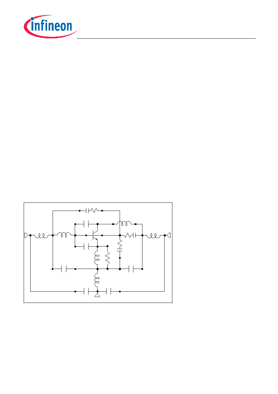
Package Equivalent Circuit:
LBC =
0.1
nH
LCC =
0.2
nH
LEC =
20
pH
LBB =
0.411
nH
LCB =
0.696
nH
LEB =
21
pH
CBEC = 0.1
pF
CBCC = 1
fF
CES =
0.34
pF
CBS =
39
fF
CCS =
75
fF
CCEO = 0.177
pF
CBEO = 92
fF
CCEI =
0.217
pF
CBEI =
52
fF
REC
=
2
RBS =
3.5
m
RCS =
1.65
m
RES =
90
B
C
E
CCEO
CBEO
CCEI
CBEI
CBEC
CBCC
S
C
B
E
LBC
LCC
LEC
CBS
RCS
RES
LBB
LCB
LEB
RBS
CCS
CES
REC
BFP740F_Chip
Valid up to 6GHz
For examples and ready to use parameters
please contact your local Infineon Technologies
distributor or sales office to obtain a Infineon
Technologies CD-ROM or see Internet:
http://www.infineon.com
2005-11-08
BFP740F
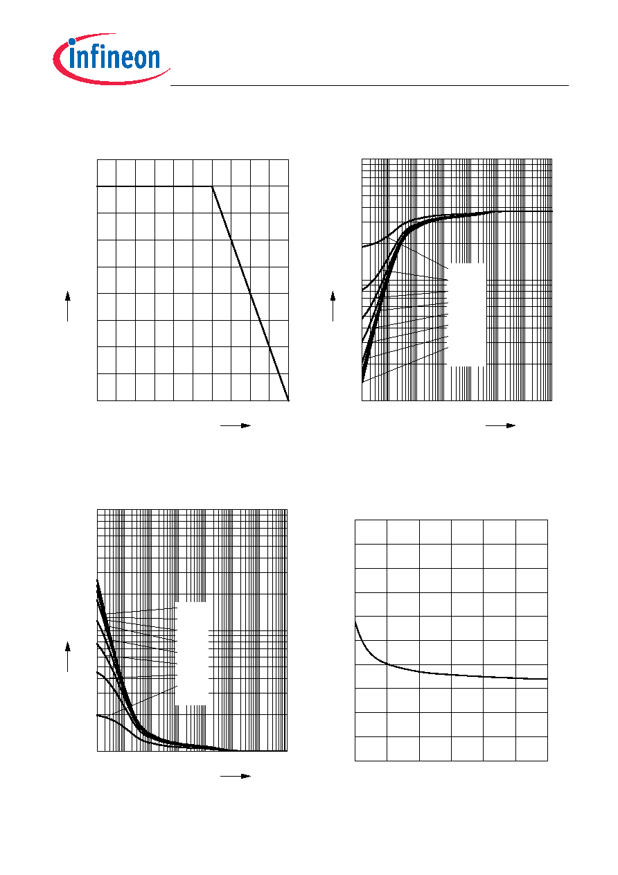
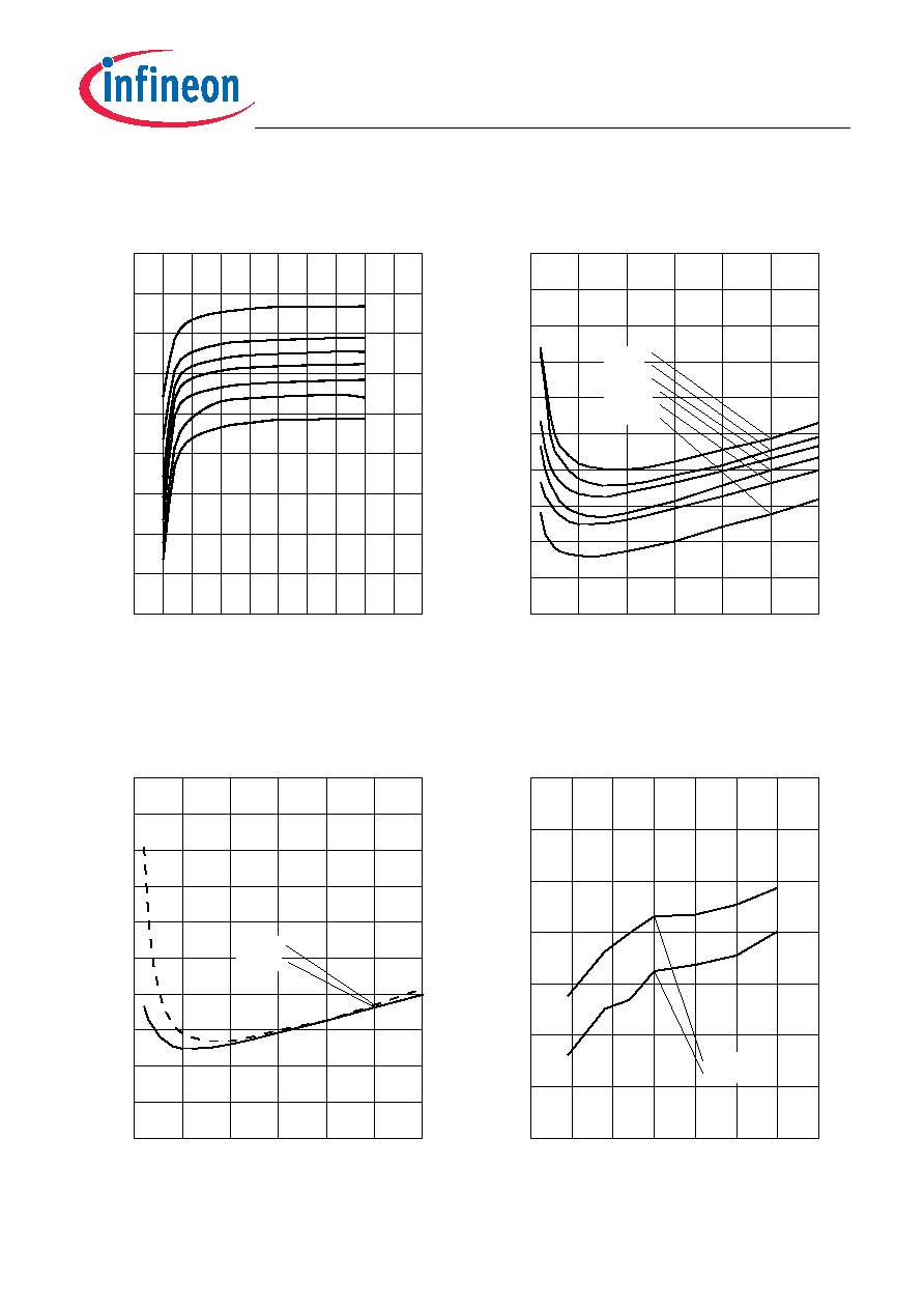
5
Total power dissipation P
tot
=
(
T
S
)
0
15
30
45
60
75
90 105 120 įC
150
T
S
0
20
40
60
80
100
120
140
mW
180
P
tot
Permissible Pulse Load R
thJS
=
(
t
p
)
10
-7
10
-6
10
-5
10
-4
10
-3
10
-2
10
0
s
t
p
1
10
2
10
3
10
K/W
R
thJS
D = 0,5
0,2
0,1
0,05
0,02
0,01
0,005
0
Permissible Pulse Load
P
totmax
/
P
totDC
=
(
t
p
)
10
-7
10
-6
10
-5
10
-4
10
-3
10
-2
10
0
s
t
p
0
10
1
10
2
10
-
P
totmax
/
P
totDC
D = 0
0.005
0.01
0.02
0.05
0.1
0.2
0.5
Collector-base capacitance C
cb
=
(
V
CB
)
f = 1 MHz
0
2
4
6
8
10
12
0
0.02
0.04
0.06
0.08
0.1
0.12
0.14
0.16
0.18
0.2
V
CB
[V]
C
cb
[pF]

2005-11-08
BFP740F
6
Third order Intercept Point IP
3
=
(
I
C
)
(Output,
Z
S
=
Z
L
= 50
)
V
CE
= parameter,
f = 900 MHz
0
5
10
15
20
25
30
35
0
3
6
9
12
15
18
21
24
27
30
I
C
[mA]
IP
3
[dBm]
1.00V
2.00V
3.00V
4.00V
Transition frequency f
T
=
(
I
C
)
V
CE
= parameter in V,
f = 2 GHz
0
5
10
15
20
25
30
35
0
5
10
15
20
25
30
35
40
45
50
I
C
[mA]
f
T
[GHz]
2V to 4V
1.00V
0.75V
0.50V
Power gain G
ma
,
G
ms
=
(
f)
V
CE
= 3 V,
I
C
= 25 mA
0
1
2
3
4
5
6
5
10
15
20
25
30
35
40
45
50
55
f [GHz]
[GHz]
G [dB]
G
ms
G
ma
|S
21
|
2
Power gain G
ma
,
G
ms
=
(
I
C
)
V
CE
= 3 V
f = parameter in GHz
0
5
10
15
20
25
30
35
10
12
14
16
18
20
22
24
26
28
30
32
34
I
C
[mA]
G [dB]
6.00GHz
5.00GHz
4.00GHz
3.00GHz
2.40GHz
1.80GHz
0.90GHz
2005-11-08
BFP740F
7
Power gain G
ma
,
G
ms
=
(
V
CE
)
I
C
= 25 mA
f = parameter in GHz
0
0.5
1
1.5
2
2.5
3
3.5
4
4.5
5
0
4
8
12
16
20
24
28
32
36
V
CE
[V]
G [dB]
6.00GHz
5.00GHz
4.00GHz
3.00GHz
2.40GHz
1.80GHz
0.90GHz
Noise figure F =
(
I
C
)
V
CE
= 3 V,
f = parameter in GHz
Z
S
=
Z
Sopt
0
5
10
15
20
25
30
0
0.2
0.4
0.6
0.8
1
1.2
1.4
1.6
1.8
2
F [dB]
I
c
[mA]
f = 0.9GHz
f = 3GHz
f = 2.4GHz
f = 6GHz
f = 5GHz
f = 1.8GHz
Noise figure F =
(
I
C
)
V
CE
= 3 V,
f = 1.8 GHz
0
5
10
15
20
25
30
0
0.2
0.4
0.6
0.8
1
1.2
1.4
1.6
1.8
2
I
c
[mA]
F [dB]
Z
S
= 50
Z
S
= Z
Sopt
Noise figure F =
(
f)
V
CE
= 3 V,
Z
S
=
Z
Sopt
0
1
2
3
4
5
6
7
0
0.2
0.4
0.6
0.8
1
1.2
1.4
F [dB]
f [GHz]
I
C
= 25mA
I
C
= 8mA
2005-11-08
BFP740F
8
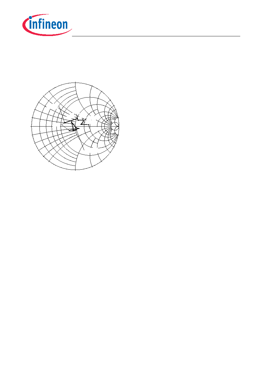
Source impedance for min.
noise figure vs. frequency
V
CE
= 3 V,
I
C
= 8 mA / 25 mA
1
0.2
0.4
2
4
0
1
-1
-5
10
1.5
-10
-1.5
0.5
-0.5
0.1
2
-0.1
-2
0.2
-0.2
0.3
3
-0.3
-3
0.4
-0.4
4
-4
5
3GHz
I
c
= 8mA
1.8GHz
6GHz
5GHz
0.9GHz
I
c
= 25mA
4GHz
2.4GHz
2005-11-08
BFP740F
9
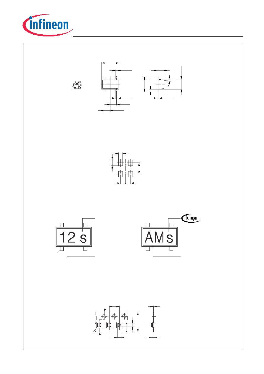
Package TSFP-4
P a c k a g e O u t l i n e
F o o t P r i n t
M a r k i n g L a y o u t
S t a n d a r d P a c k i n g
Reel Ý180 mm = 3.000 Pieces/Reel
Reel Ý330 mm = 10.000 Pieces/Reel
Manufacturer
Type code
BFP420F
Example
Pin 1
0.35
0.45
0.9
0.5
0.5
4
0.2
1.55
0.7
1.4
8
Pin 1
Ī0.05
0.2
Ī0.05
1.4
1
2
10į MAX.
Ī0.05
0.8
1.2
Ī0.05
Ī0.04
0.55
Ī0.05
0.2
Ī0.05
0.15
Ī0.05
0.2
0.5
Ī0.05
0.5
Ī0.05
4
3

2005-11-08
BFP740F
10
Published by Infineon Technologies AG,
St.-Martin-Strasse 53,
81669 MŁnchen
© Infineon Technologies AG 2005.
All Rights Reserved.
Attention please!
The information herein is given to describe certain components and shall not be
considered as a guarantee of characteristics.
Terms of delivery and rights to technical change reserved.
We hereby disclaim any and all warranties, including but not limited to warranties of
non-infringement, regarding circuits, descriptions and charts stated herein.
Information
For further information on technology, delivery terms and conditions and prices
please contact your nearest Infineon Technologies Office (www.Infineon.com).
Warnings
Due to technical requirements components may contain dangerous substances.
For information on the types in question please contact your nearest Infineon
Technologies Office.
Infineon Technologies Components may only be used in life-support devices or
systems with the express written approval of Infineon Technologies, if a failure of
such components can reasonably be expected to cause the failure of that life-support
device or system, or to affect the safety or effectiveness of that device or system.
Life support devices or systems are intended to be implanted in the human body, or
to support and/or maintain and sustain and/or protect human life. If they fail, it is
reasonable to assume that the health of the user or other persons may be endangered.