Jun-11-2003
1
BFS386L6
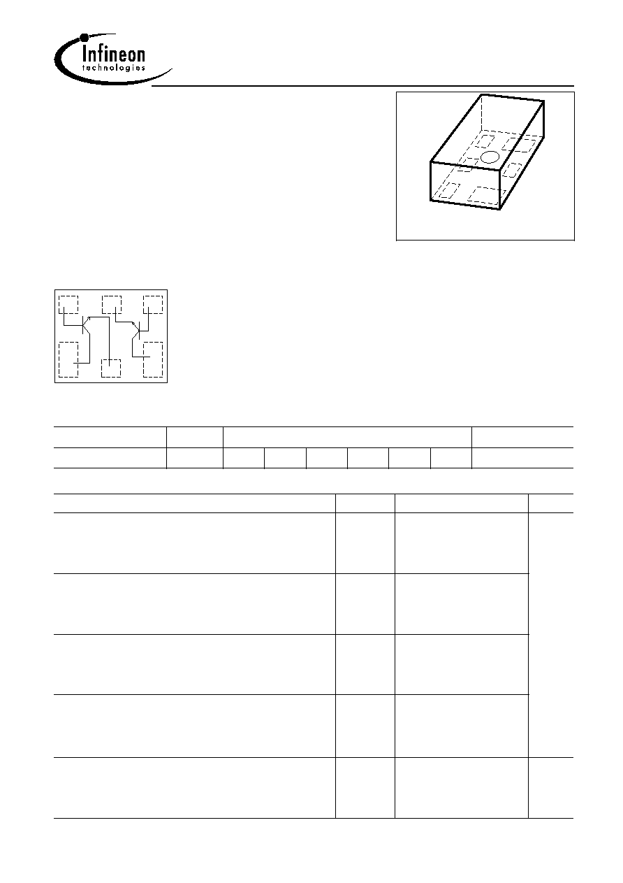
P-TSLP-6-1
1
2
3
4
5
6
NPN Silicon RF Transistor
Preliminary data
Low voltage/ low current operation
For low noise amplifiers
For oscillators up to 3.5 GHz and Pout > 10 dBm
Low noise figure: TR1: 1.0dB at 1.8 GHz
TR2: 1.1 dB at 1.8 GHz
Built in 2 Transistors (TR1: die as BFR360L3,
TR2: die as BFR380L3)
T R 1
T R 2
1
2
3
4
5
6
ESD
: Electrostatic discharge sensitive device, observe handling precaution!
Type
Marking
Pin Configuration
Package
BFS386L6
FD
1=C1 2=E1 3=C2 4=B2 5=E2 6=B1 TSLP-6-1
Maximum Ratings
Parameter
Symbol
Value
Unit
Collector-emitter voltage
TR1
TR2
V
CEO
6
6
V
Collector-emitter voltage
TR1
TR2
V
CES
15
15
Collector-base voltage
TR1
TR2
V
CBO
15
15
Emitter-base voltage
TR1
TR2
V
EBO
2
2
Collector current
TR1
TR2
I
C
35
80
mA

Jun-11-2003
2
BFS386L6
Maximum Ratings
Parameter
Symbol
Value
Unit
Base current
TR1
TR2
I
B
4
14
mA
Total power dissipation
1)
T
S
101∞C, TR1
T
S
96∞C, TR2
P
tot
210
380
mW
Junction temperature
TR1
TR2
T
j
150
150
∞C
Ambient temperature
TR1
TR2
T
A
-65 ... 150
-65 ... 150
Storage temperature
TR1
TR2
T
stg
-65 ... 150
-65 ... 150
Thermal Resistance
Parameter
Symbol
Value
Unit
Junction - soldering point
2)
TR1
TR2
R
thJS
230
140
K/W
1TS is measured on the collector lead at the soldering point to the pcb
2For calculation of RthJA please refer to Application Note Thermal Resistance
Jun-11-2003
3
BFS386L6
Electrical Characteristics at T
A
= 25∞C, unless otherwise specified
Parameter
Symbol
Values
Unit
min.
typ.
max.
DC Characteristics
Collector-emitter breakdown voltage
TR1, I
C
= 1 mA, I
B
= 0
TR2, I
C
= 1mA, I
B
= 0
V
(BR)CEO
6
6
9
9
-
-
V
Collector-emitter cutoff current
TR1, V
CE
= 15 V , V
BE
= 0
TR2, V
CE
= 15 V , V
BE
= 0
I
CES
-
-
-
-
10
10
µA
Collector-base cutoff current
TR1, V
CB
= 5 V, I
E
= 0
TR2, V
CB
= 5 V, I
E
= 0
I
CBO
-
-
-
-
100
100
nA
Emitter-base cutoff current
TR1, V
EB
= 1 V, I
C
= 0
TR2, V
EB
= 1 V, I
C
= 0
I
EBO
-
-
-
-
1
1
µA
DC current gain-
TR1, I
C
= 15 mA, V
CE
= 3 V
TR2, I
C
= 40 mA, V
CE
= 3 V
h
FE
60
60
130
130
200
200
-
Electrical Characteristics at T
A
= 25∞C, unless otherwise specified
Parameter
Symbol
Values
Unit
min.
typ.
max.
AC Characteristics (verified by random sampling)
Transition frequency
TR1, I
C
= 15 mA, V
CE
= 3 V, f = 1 GHz
TR2, I
C
= 40 mA, V
CE
= 3 V, f = 1 GHz
f
T
-
-
14
14
-
-
GHz
Collector-base capacitance
TR1, V
CB
= 5 V, f = 1 MHz, emitter grounded
TR2, V
CB
= 5 V, f = 1 MHz, emitter grounded
C
cb
-
-
0.3
0.5
-
-
pF
Collector emitter capacitance
TR1, V
CE
= 5 V, f = 1 MHz, base grounded
TR2, V
CE
= 5 V, f = 1 MHz, base grounded
C
ce
-
-
0.15
0.2
-
-
Emitter-base capacitance
TR1, V
EB
= 0,5 V, f = 1 MHz, collector grounded
TR2, V
EB
= 0,5 V, f = 1 MHz, collector grounded
C
eb
-
-
0.43
1.1
-
-

Jun-11-2003
4
BFS386L6
Electrical Characteristics at TA = 25∞C, unless otherwise specified
Parameter
Symbol
Values
Unit
min.
typ.
max.
AC Characteristics (verified by random sampling)
Noise figure
TR1, I
C
= 3 mA, V
CE
= 3 V, Z
S
= Z
Sopt
,
f = 1.8 GHz
TR1, I
C
= 3 mA, V
CE
= 3 V, Z
S
= Z
Sopt
,
f = 3 GHz
TR2, I
C
= 8 mA , V
CE
= 3 V, Z
S
= Z
Sopt
,
f = 1.8 GHz
TR2, I
C
= 8 mA , V
CE
= 3 V, Z
S
= Z
Sopt
,
f = 3 GHz
F
-
-
-
-
1
1.6
1.3
1.9
-
-
-
-
dB
Power gain, maximum available
1)
TR1, I
C
= 15 mA, V
CE
= 3 V, f = 1.8 GHz
TR1, I
C
= 15 mA, V
CE
= 3 V, f = 3 GHz
TR2, I
C
= 40 mA, V
CE
= 3 V, f = 1.8 GHz
TR2, I
C
= 40 mA, V
CE
= 3 V, f = 3 GHz
G
ma
-
-
-
-
14.5
10
12
8
-
-
-
-
Transducer gain
TR1, I
C
= 15 mA, V
CE
= 3 V, f = 1.8 GHz
TR1, I
C
= 15 mA, V
CE
= 3 V, f = 3 GHz
TR2, I
C
= 15 mA, V
CE
= 3 V, f = 1.8 GHz
TR2, I
C
= 15 mA, V
CE
= 3 V, f = 3 GHz
|S
21e
|
2
-
-
-
-
12
8
10
6
-
-
-
-
Third order intercept point at output
2)
TR1, V
CE
= 3 V, I
C
= 15 mA, f = 1.8 GHz
TR2, V
CE
= 3 V, I
C
= 40 mA, f = 1.8 GHz
IP
3
-
-
24
27
-
-
dBm
1dB Compression point
TR1, I
C
= 15 mA, V
CE
= 3 V, f = 1.8 GHz
TR2, I
C
= 40 mA, V
CE
= 3 V, f = 1.8 GHz
P
-1dB
-
-
9
11.5
-
-
1
G
ma
= |
S
21e
/
S
12e
| (k-(k≤-1)
1/2
)
2IP3 value depends on termination of all intermodulation frequency components.
Termination used for this measurement is 50
from 0.1 MHz to 6 GHz