 | –≠–ª–µ–∫—Ç—Ä–æ–Ω–Ω—ã–π –∫–æ–º–ø–æ–Ω–µ–Ω—Ç: BGA420 | –°–∫–∞—á–∞—Ç—å:  PDF PDF  ZIP ZIP |
BGA420
Jan-29-2002
1
in SIEGET 25-Technologie
Si-MMIC-Amplifier
Cascadable 50 -gain block
Unconditionally stable
Gain |S
21
|
2
= 13 dB at 1.8 GHz
IP
3out
= +13 dBm at 1.8 GHz
(V
D
= 3 V, I
D
= typ. 6.7 mA)
Noise figure NF = 2.3 dB at 1.8 GHz
Reverse isolation > 28 dB and
return loss IN / OUT > 12 dB at 1.8 GHz
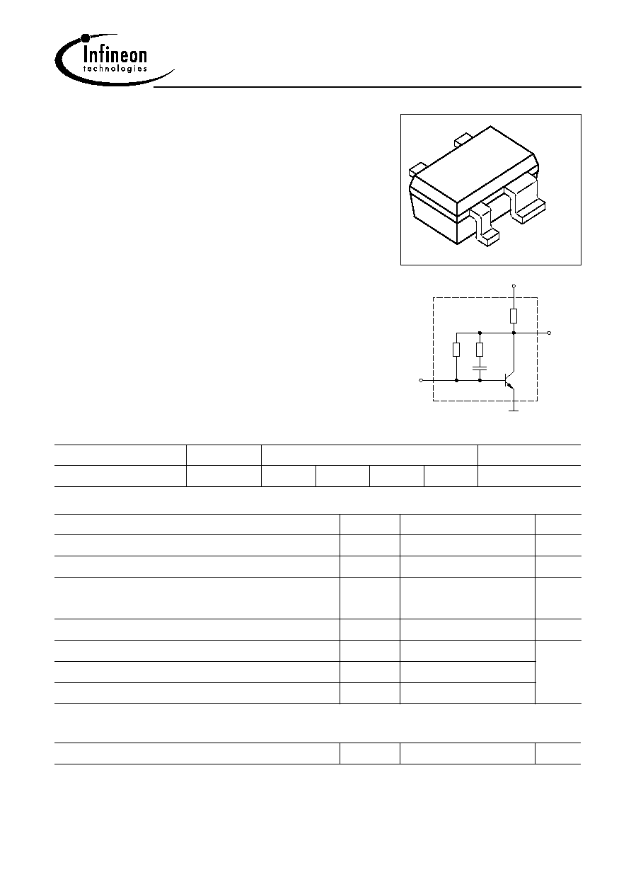
VPS05605
4
2
1
3
EHA07385
D
V
4
2
1
IN
OUT
3
GND
Circuit Diagram
ESD: Electrostatic discharge sensitive device, observe handling precaution!
Type
Marking
Pin Configuration
Package
BGA420
BLs
1, IN
2, GND 3, OUT 4, VD
SOT343
Maximum Ratings
Parameter
Symbol
Value
Unit
Device current
I
D
15
mA
Device voltage
V
D
6
V
Total power dissipation
T
S
= 110 ∞C
P
tot
90
mW
RF input power
P
RFin
0
dBm
Junction temperature
T
j
150
∞C
Ambient temperature
T
A
-65 ... 150
Storage temperature
T
stg
-65 ... 150
Thermal Resistance
Junction - soldering point
1)
R
thJS
410
K/W
1For calculation of R
thJA
please refer to Application Note Thermal Resistance
BGA420
Jan-29-2002
2
Electrical Characteristics at T
A
= 25 ∞C, unless otherwise specified.
Parameter
Symbol
Values
Unit
min.
typ.
max.
AC characteristics V
D
= 3 V, Z
o
= 50
Device current
I
D
5.4
6.7
8
mA
Insertion power gain
f
= 0.1 GHz
f
= 1 GHz
f
= 1.8 GHz
|S
21
|
2
17
15
11
19
17
13
-
-
-
dB
Reverse isolation
f
= 1.8 GHz
S12
25
28
-
Noise figure
f
= 0.1 GHz
f
= 1 GHz
f
= 1.8 GHz
NF
-
-
-
1.9
2.2
2.3
2.3
2.6
2.7
Intercept point at the output
f
= 1 GHz
IP
3out
10
13
-
dBm
1dB compression point
f
= 1 GHz
P
-1dB
-6
-2.5
-
Return loss input
f
= 1.8 GHz
RL
in
8
11
-
dB
Return loss output
f
= 1.8 GHz
RL
out
12
16
-
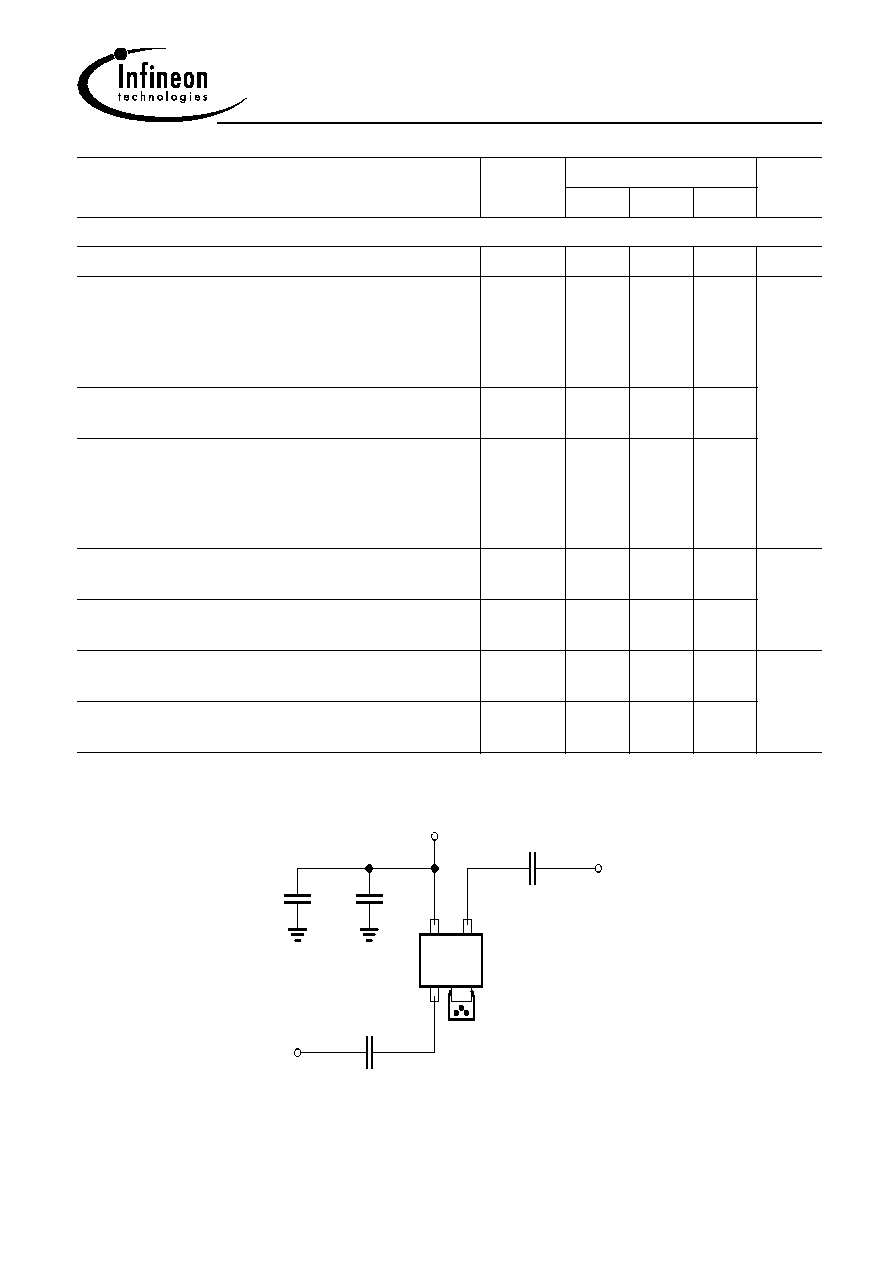
Typical biasing configuration
EHA07386
100 pF
RF IN
100 pF
GND
RF OUT
10 nF
100 pF
+
3
1
2
4
D
V
BGA 420
Note: 1) Large-value capacitors should be connected from pin 4 to ground right at the device
to provide a low impedance path.
2) The use of plated through holes right at pin 2 is essential for pc-board-applications. Thin
boards are recommended to minimize the parasitic inductance to ground.
BGA420
Jan-29-2002
3
Typical S-Parameters at T
A
= 25 ∞C
f
S
11
S
21
S
12
S
22
GHz
MAG
ANG
MAG
ANG
MAG
ANG
MAG
ANG
V
D
= 3 V, Z
o
= 50
0.1
0.5
0.8
1
1.5
1.8
1.9
2
2.4
3
0.5686
0.5066
0.4404
0.3904
0.2841
0.2343
0.2136
0.2062
0.1688
0.1558
-8.5
-19.2
-28.7
-34.6
-50.5
-60.6
-64.1
-68.4
-89.7
-104.9
9.314
8.393
7.352
6.69
5.244
4.567
4.355
4.165
3.417
2.861
170.6
149.4
135.2
126.8
111.1
104
102
99.7
91.7
85.3
0.0268
0.0248
0.0236
0.024
0.0314
0.0378
0.0406
0.0426
0.0549
0.0682
12.7
11.7
25.6
35.9
57.2
63.5
66.1
67.2
71.4
73.1
0.2808
0.2613
0.2361
0.2144
0.1398
0.0979
0.0838
0.0689
0.0224
0.0284
-8.6
-3.8
-6.7
-9
-15
-18.2
-21.5
-22.2
-48
-147.5
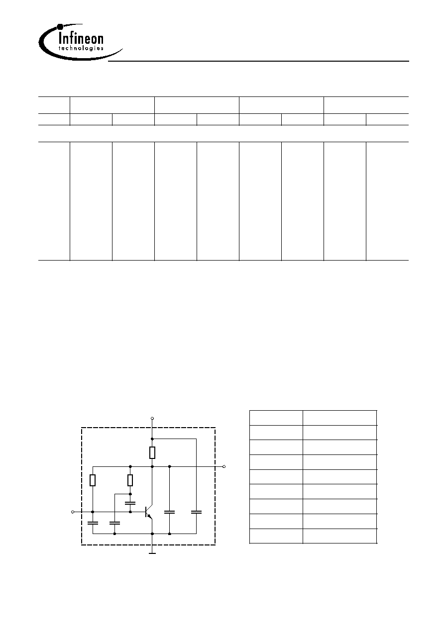
Spice-model BGA 420
EHA07387
3
R
R
1
P1
C
P2
C
1
C
R
2
P3
C
C
P4
11
13
14
12
including parasitics
OUT
BGA 420-chip
IN
GND
+V
T1
T1
T501
R
1
14.5k
R
2
140
R
3
2.4k
C
1
2.3pF
C
P1
0.2pF
C
P2
0.2pF
C
P3
0.6pF
C
P4
0.1pF
BGA420
Jan-29-2002
4
Transistor Chip Data T1 (Berkley-SPICE 2G.6 Syntax) :
BF =
83.23
-
IKF =
0.16493
A
BR =
10.526
-
IKR =
0.25052
A
RB =
15
RE =
1.9289
VJE =
0.70367
V
XTF =
0.3641
-
PTF =
0
deg
MJC =
0.48652
-
CJS =
0
fF
XTB =
0
-
FC =
0.99469
-
NF =
1.0405
-
ISE =
15.761
fA
NR =
0.96647
-
ISC =
0.037223
fA
IRB =
0.21215
A
RC =
0.12691
MJE =
0.37747
-
VTF =
0.19762
V
CJC =
96.941
fF
XCJC =
0.08161
-
VJS =
0.75
V
EG =
1.11
eV
TNOM
300
K
IS =
0.21024
fA
VAF =
39.251
V
NE =
1.7763
-
VAR =
34.368
V
NC =
1.3152
-
RBM =
1.3491
CJE =
3.7265
fF
TF =
4.5899
ps
ITF =
1.3364
mA
VJC =
0.99532
V
TR =
1.4935
ns
MJS =
0
-
XTI =
3
-
C'-E'-Diode Data (Berkley-SPICE 2G.6 Syntax) :
RS =
20
IS =
2
fA
N =
1.02
-
All parameters are ready to use, no scaling is necessary
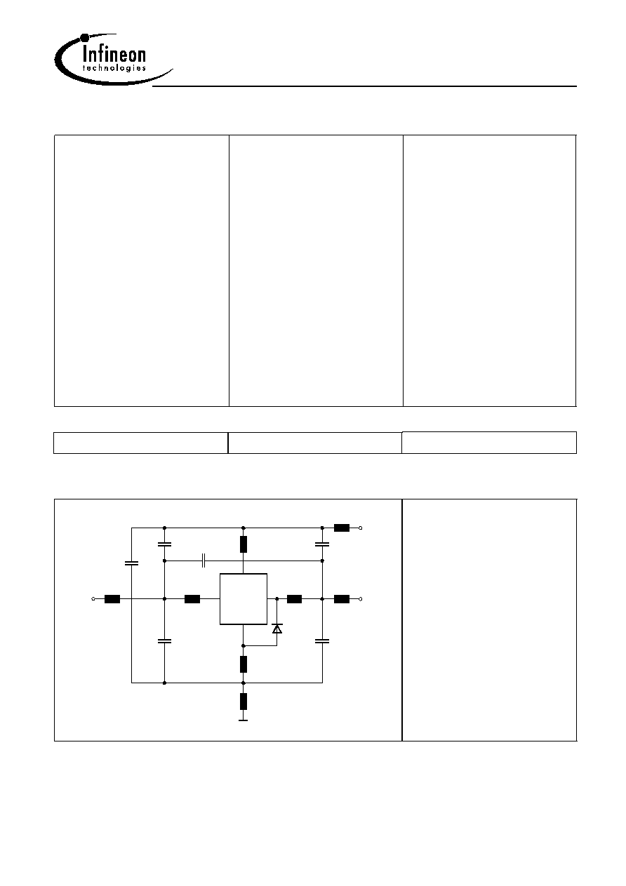
Package Equivalent Circuit:
L
BI
=
0.36
nH
L
BO
=
0.4
nH
L
EI
=
0.3
nH
L
EO
=
0.15
nH
L
CI
=
0.36
nH
L
CO
=
0.4
nH
C
BE
=
95
fF
C
CB
=
6
fF
C
CE
=
132
fF
C
1
=
28
fF
C
2
=
88
fF
C
3
=
8
fF
L
1
=
0.6
nH
L
2
=
0.4
nH
EHA07388
L
BI
1
C
BE
C
BO
L
OUT
EI
L
L
EO
CB
C
CI
L
C
3
CO
L
CE
C
Chip
C'-E'-
IN
Diode
C
2
2
L
L
1
GND
+V
12
13
14
11
BGA 420
Valid up to 3GHz
Extracted on behalf of Infineon Technologies AG by:
Institut f¸r Mobil-und Satellitentechnik (IMST)
For examples and ready to use parameters please contact your local Infineon Technologies distributor
or sales office to obtain a Infineon Technologies CD-ROM or see Internet:
http://www.infineon.com/silicondiscretes
BGA420
Jan-29-2002
5
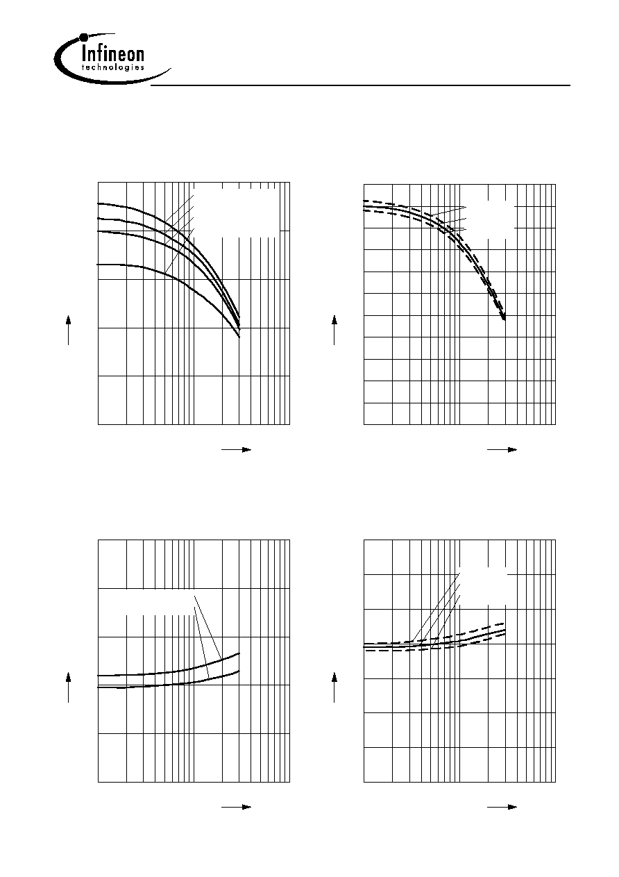
Insertion power gain |S
21
|
2
= f (f)
V
D
= 3 V
T
A
= parameter
10
-1
10
0
10
1
GHz
f
0
2
4
6
8
10
12
14
16
18
dB
22
|
S
21
|
2
TA=-20∞C
TA=+25∞C
TA=+75∞C
Insertion power gain |S
21
|
2
= f (f)
V
D
, I
D
= parameter
10
-1
10
0
10
1
GHz
f
0
5
10
15
dB
25
|
S
21
|
2
VD=5V, ID=12.4mA
VD=4V, ID=9.4mA
VD=3V, ID=6.4mA
VD=2V, ID=3,4mA
Noise figure NF = f (f)
V
D
,I
D
= parameter
10
-1
10
0
10
1
GHz
f
0
1
2
3
dB
5
NF
VD=5V, ID=12.4mA
VD=3V, ID=6.4mA
Noise figure NF = f (f)
V
D
= 3V
T
A
= parameter
10
-1
10
0
10
1
GHz
f
0.0
0.5
1.0
1.5
2.0
2.5
dB
3.5
NF
TA=+75∞C
TA=+25∞C
TA=-20∞C