 | –≠–ª–µ–∫—Ç—Ä–æ–Ω–Ω—ã–π –∫–æ–º–ø–æ–Ω–µ–Ω—Ç: BSP170P | –°–∫–∞—á–∞—Ç—å:  PDF PDF  ZIP ZIP |

2002-01-16
Page 1
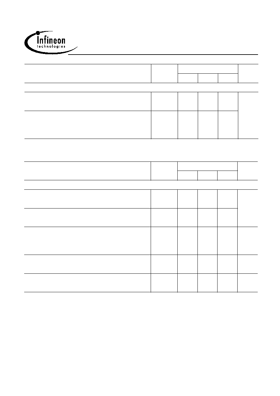
Final data
BSP 170 P
SIPMOS
Small-Signal-Transistor
Product Summary
V
DS
-60
V
R
DS(on)
0.3
I
D
-1.9
A
Feature
∑
P-Channel
∑
Enhancement mode
∑
Avalanche rated
∑
dv/dt rated
SOT-223
VPS05163
1
2
3
4
Gate
pin1
Drain
pin 2
Source
pin 3
Type
Package
Ordering Code
BSP 170 P
SOT-223
Q67041-S4018
Maximum Ratings
,at T
j
= 25 ∞C, unless otherwise specified
Parameter
Symbol
Value
Unit
Continuous drain current
T
A
=25∞C
T
A
=70∞C
I
D
-1.9
-1.5
A
Pulsed drain current
T
A
=25∞C
I
D puls
-7.6
Avalanche energy, single pulse
I
D
=-1.9 A ,
V
DD
=-25V,
R
GS
=25
E
AS
70
mJ
Avalanche energy, periodic limited by T
jmax
E
AR
0.18
Reverse diode dv/dt
I
S
=-1.9A,
V
DS
=-48V, d
i
/d
t
=-200A/µs,
T
jmax
=150∞C
dv/dt
-6
kV/µs
Gate source voltage
V
GS
±20
V
Power dissipation
T
A
=25∞C
P
tot
1.8
W
Operating and storage temperature
T
j ,
T
stg
-55... +150
∞C
IEC climatic category; DIN IEC 68-1
55/150/56
2002-01-16
Page 2
Final data
BSP 170 P
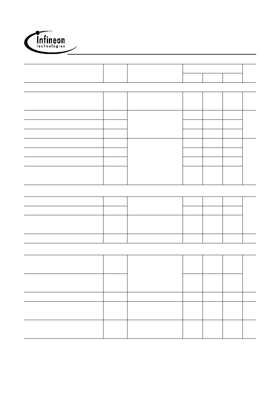
Thermal Characteristics
Parameter
Symbol
Values
Unit
min.
typ.
max.
Characteristics
Thermal resistance, junction - soldering point
(Pin 4)
R
thJS
-
-
20
K/W
SMD version, device on PCB:
@ min. footprint
@ 6 cm
2
cooling area
1)
R
thJA
-
-
-
-
110
70
Electrical Characteristics, at T
j
= 25 ∞C, unless otherwise specified
Parameter
Symbol
Values
Unit
min.
typ.
max.
Static Characteristics
Drain-source breakdown voltage
V
GS
=0, I
D
=-250µA
V
(BR)DSS
-60
-
-
V
Gate threshold voltage, V
GS
= V
DS
I
D
=-250µA
V
GS(th)
-2.1
-3
-4
Zero gate voltage drain current
V
DS
=-60V, V
GS
=0, T
j
=25∞C
V
DS
=-60V, V
GS
=0, T
j
=125∞C
I
DSS
-
-
-0.1
-10
-1
-100
µA
Gate-source leakage current
V
GS
=-20V, V
DS
=0
I
GSS
-
-10
-100 nA
Drain-source on-state resistance
V
GS
=-10V, I
D
=-1.9
R
DS(on)
-
0.24
0.3
1Device on 40mm*40mm*1.5mm epoxy PCB FR4 with 6cm≤ (one layer, 70 µm thick) copper area for drain
connection. PCB is vertical without blown air.
2002-01-16
Page 3
Final data
BSP 170 P
Electrical Characteristics, at T
j
= 25 ∞C, unless otherwise specified
Parameter
Symbol
Conditions
Values
Unit
min.
typ.
max.
Dynamic Characteristics
Transconductance
g
fs
V
DS
2*I
D
*R
DS(on)max
,
I
D
=-1.9
1.4
2.8
-
S
Input capacitance
C
iss
V
GS
=0, V
DS
=-25V,
f=1MHz
-
328
410
pF
Output capacitance
C
oss
-
105
135
Reverse transfer capacitance
C
rss
-
38
48
Turn-on delay time
t
d(on)
V
DD
=-30V, V
GS
=-10V,
I
D
=-1.9A, R
G
=6
-
14
21
ns
Rise time
t
r
-
28
42
Turn-off delay time
t
d(off)
-
92
138
Fall time
t
f
-
60
90
Gate Charge Characteristics
Gate to source charge
Q
gs
V
DD
=-48V, I
D
=-1.9A
-
-1.4
-2.1
nC
Gate to drain charge
Q
gd
-
-3.6
-5.4
Gate charge total
Q
g
V
DD
=-48V, I
D
=-1.9A,
V
GS
=0 to -10V
-
-12.5
-16
Gate plateau voltage
V
(plateau) V
DD
=-48V, I
D
=-1.9A
-
-3.85
-
V
Reverse Diode
Inverse diode continuous
forward current
I
S
T
A
=25∞C
-
-
-1.9
A
Inverse diode direct current,
pulsed
I
SM
-
-
-7.6
Inverse diode forward voltage V
SD
V
GS
=0, I
F
=-1.9A
-
-0.85
-1.1
V
Reverse recovery time
t
rr
V
R
=-30V, I
F=
l
S
,
di
F
/dt=-100A/µs
-
36
54
ns
Reverse recovery charge
Q
rr
V
R
=-30V, I
F=
l
S
,
di
F
/dt=100A/µs
-
41
62
nC

2002-01-16
Page 4
Final data
BSP 170 P
1 Power dissipation
P
tot
= f (TA)
0
20
40
60
80
100
120
∞C
160
T
A
0
0.2
0.4
0.6
0.8
1
1.2
1.4
1.6
W
1.9
BSP 170 P
P
tot
2 Drain current
I
D
= f (TA)
parameter: |V
GS
|
10V
0
20
40
60
80
100
120
∞C
160
T
A
0
-0.2
-0.4
-0.6
-0.8
-1
-1.2
-1.4
-1.6
A
-2
BSP 170 P
I
D
3 Safe operating area
I
D
= f ( V
DS
)
parameter : D = 0 , TA = 25∞C
-10
-1
-10
0
-10
1
-10
2
V
V
DS
-2
-10
-1
-10
0
-10
1
-10
A
BSP 170 P
I
D
R
D
S(
on
)
=
V
D
S
/
I
D
DC
10 ms
1 ms
tp = 340.0µs
4 Transient thermal impedance
Z
thJS
= f (t
p
)
parameter : D = t
p
/T
10
-7
10
-6
10
-5
10
-4
10
-3
10
-2
10
-1
10
1
s
t
p
-5
10
-4
10
-3
10
-2
10
-1
10
0
10
1
10
2
10
K/W
BSP 170 P
Z
thJS
single pulse
0.01
0.02
0.05
0.10
0.20
D = 0.50

2002-01-16
Page 5
Final data
BSP 170 P
5 Typ. output characteristic
I
D
= f (V
DS
); T
j
=25∞C
parameter: t
p
= 80 µs
0
-0.5 -1 -1.5 -2 -2.5 -3 -3.5 -4
V
-5
V
DS
0
-0.5
-1
-1.5
-2
-2.5
-3
-3.5
-4
A
-5
BSP 170 P
I
D
VGS [V]
a
a
-4.0
b
b
-4.5
c
c
-5.0
d
d
-5.5
e
e
-6.0
f
f
-6.5
g
P
tot
= 1.8W
g
-7.0
6 Typ. drain-source on resistance
R
DS(on)
= f (I
D
)
parameter: V
GS
0
-0.4 -0.8 -1.2 -1.6
-2
-2.4 -2.8
A
-3.4
I
D
0
0.1
0.2
0.3
0.4
0.5
0.6
0.7
0.8
1
BSP 170 P
R
DS(on)
V
GS
[V] =
a
a
-4.0
b
b
-4.5
c
c
-5.0
d
d
-5.5
e
e
-6.0
f
f
-6.5
g
g
-7.0
7 Typ. transfer characteristics
I
D
= f ( V
GS
); V
DS
2 x I
D
x R
DS(on)max
parameter: t
p
= 80 µs
0
1
2
3
4
5
6
V
8
- V
GS
0
2
4
6
8
10
12
A
16
-
I
D
8 Typ. forward transconductance
g
fs
= f(I
D
); T
j
=25∞C
parameter: tp = 80 µs
0
3
6
9
A
15
- I
D
0
1
2
3
4
S
6
gfs