1999-09-22
Page 1
BSP308
Preliminary data
SIPMOS
Æ
Small-Signal-Transistor
Features
∑
N-Channel
∑
Enhancement mode
∑
Logic Level
∑
d
v/dt rated
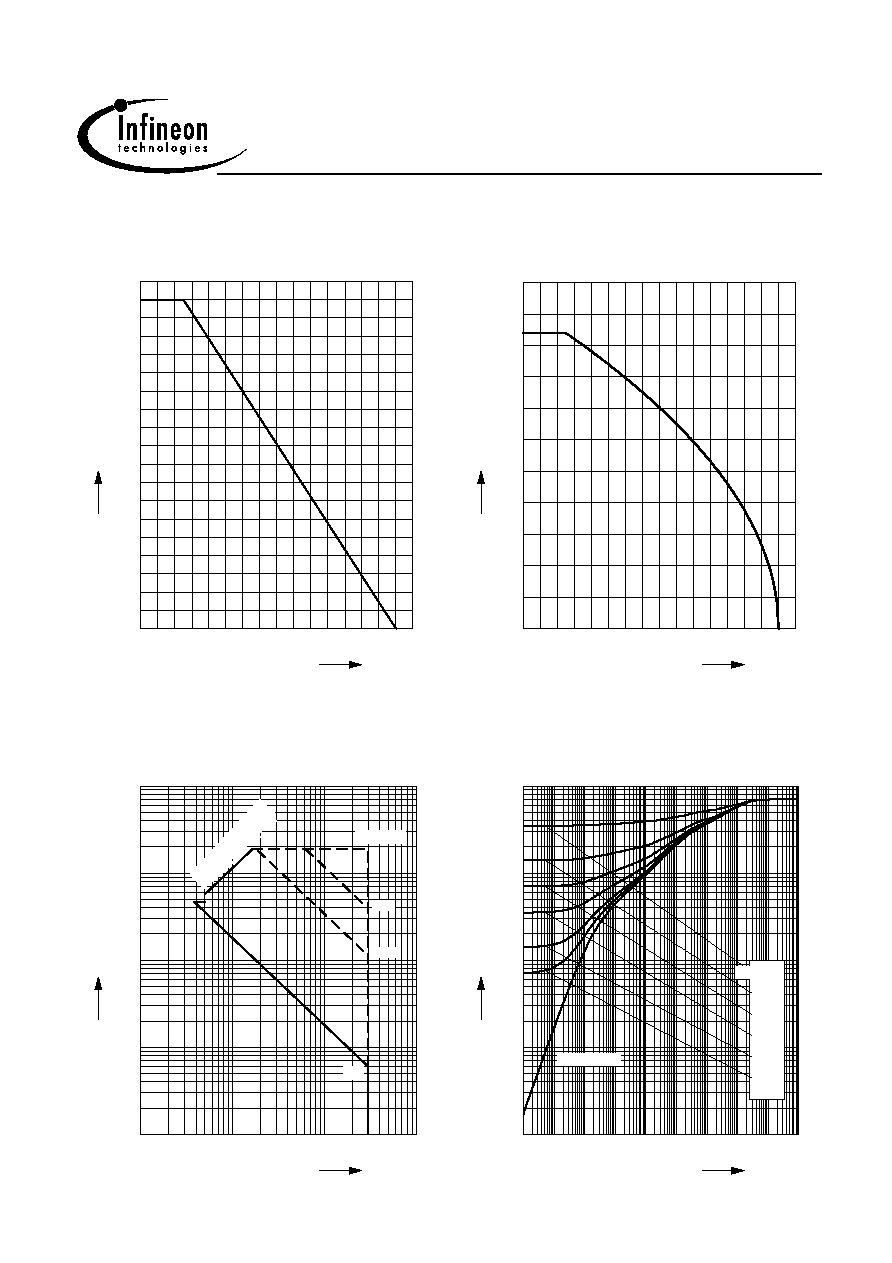
Product Summary
Drain source voltage
V
V
DS
30
Drain-Source on-state resistance
R
DS(on)
0.05
Continuous drain current
A
I
D
4.7
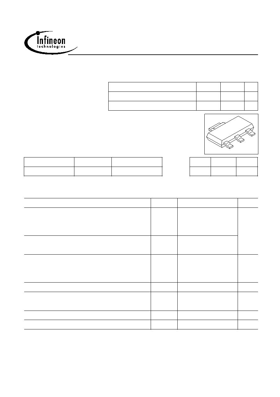
VPS05163
1
2
3
4
Type
Package
Ordering Code
BSP308
SOT-223
Q67000-S4011
Pin 1
Pin 2/4
PIN 3
G
D
S
Maximum Ratings,at
T
j
= 25 ∞C, unless otherwise specified
Parameter
Symbol
Unit
Value
4.7
3.9
A
Continuous drain current
T
A
= 25 ∞C
T
A
= 70 ∞C
I
D
Pulsed drain current
T
A
= 25 ∞C
I
D puls
18.8
d
v/dt
6
Reverse diode d
v/dt
I
S
= 4.7 A,
V
DS
= 20 V, d
i/dt = 200 A/µs,
T
jmax
= 150 ∞C
kV/µs
Gate source voltage
V
GS
±20
V
Power dissipation
T
A
= 25 ∞C
P
tot
1.8
W
Operating and storage temperature
T
j ,
T
stg
-55...+150
∞C
IEC climatic category; DIN IEC 68-1
55/150/56
1999-09-22
Page 2
BSP308
Preliminary data
Thermal Characteristics
Parameter
Symbol
Unit
Values
min.
max.
typ.
Characteristics
Thermal resistance, junction - soldering point
25
K/W
-
R
thJS
-
SMD version, device on PCB:
@ min. footprint
@ 6 cm
2
cooling area
1)
R
thJA
-
-
-
-
110
70
K/W
Electrical Characteristics, at
T
j
= 25 ∞C, unless otherwise specified
Parameter
Symbol
Values
Unit
min.
typ.
max.
Static Characteristics
Drain- source breakdown voltage
V
GS
= 0 V,
I
D
= 250 µA
V
(BR)DSS
30
-
V
-
Gate threshold voltage,
V
GS
=
V
DS
I
D
= 20 µA
1.2
1.6
2
V
GS(th)
Zero gate voltage drain current
V
DS
= 30 V,
V
GS
= 0 V,
T
j
= 25 ∞C
V
DS
= 30 V,
V
GS
= 0 V,
T
j
= 125 ∞C
µA
1
100
I
DSS
0.1
10
-
-
I
GSS
-
10
100
Gate-source leakage current
V
GS
= 20 V,
V
DS
= 0 V
nA
Drain-Source on-state resistance
V
GS
= 4.5 V,
I
D
= 3.9 A
R
DS(on)
-
0.05
0.075
Drain-Source on-state resistance
V
GS
= 10 V,
I
D
= 4.7
R
DS(on)
-
0.03
0.05
1Device on 40mm*40mm*1.5mm epoxy PCB FR4 with 6cm2 (one layer, 70 µm thick) copper area for drain
connection. PCB is vertical without blown air.
1999-09-22
Page 3
BSP308
Preliminary data
Electrical Characteristics, at
T
j
= 25 ∞C, unless otherwise specified
Parameter
Symbol
Values
Unit
min.
typ.
max.
Dynamic Characteristics
Transconductance
V
DS
2*
I
D
*
R
DS(on)max
,
I
D
= 3.9 A
6.1
g
fs
S
-
8.8
Input capacitance
V
GS
= 0 V,
V
DS
= 25 V,
f = 1 MHz
C
iss
400
500
pF
-
C
oss
-
200
160
Output capacitance
V
GS
= 0 V,
V
DS
= 25 V,
f = 1 MHz
Reverse transfer capacitance
V
GS
= 0 V,
V
DS
= 25 V,
f = 1 MHz
90
70
C
rss
-
Turn-on delay time
V
DD
= 15 V,
V
GS
= 4.5 V,
I
D
= 3.9 A ,
R
G
= 15
-
24
ns
16
t
d(on)
Rise time
V
DD
= 15 V,
V
GS
= 4.5 V,
I
D
= 3.9 A ,
R
G
= 15
t
r
-
45
30
16
24
t
d(off)
Turn-off delay time
V
DD
= 15 V,
V
GS
= 4.5 V,
I
D
= 3.9 A ,
R
G
= 15
-
Fall time
V
DD
= 15 V,
V
GS
= 4.5 V,
I
D
= 3.9 A ,
R
G
= 15
t
f
-
15
23
1999-09-22
Page 4
BSP308
Preliminary data
Electrical Characteristics, at
T
j
= 25 ∞C, unless otherwise specified
Unit
Values
Symbol
Parameter
min.
typ.
max.
Dynamic Characteristics
Gate to source charge
V
DD
= 24 V,
I
D
= 4.7 A
-
Q
gs
nC
2.9
1.9
Gate to drain charge
V
DD
= 24 V,
I
D
= 4.7 A
Q
gd
5.4
8.1
-
22
-
Q
g
Gate charge total
V
DD
= 24 V,
I
D
= 4.7 A,
V
GS
= 0 to 10 V
14.5
Gate plateau voltage
V
DD
= 24 V ,
I
D
= 4.7 A
V
(plateau)
-
3.1
-
V
Parameter
Symbol
Values
Unit
min.
typ.
max.
Reverse Diode
Inverse diode continuous forward current
T
A
= 25 ∞C
I
S
-
-
4.7
A
Inverse diode direct current,pulsed
T
A
= 25 ∞C
I
SM
-
-
18.8
Inverse diode forward voltage
V
GS
= 0 V,
I
F
= 4.7 A
V
SD
-
0.84
1.1
V
Reverse recovery time
V
R
= 15 V,
I
F
=
I
S
, d
i
F
/d
t = 100 A/µs
t
rr
-
38.4
57.6
ns
Reverse recovery charge
V
R
= 15 V,
I
F=
l
S
, d
i
F
/d
t = 100 A/µs
Q
rr
-
22.3
33.5
nC