 | –≠–ª–µ–∫—Ç—Ä–æ–Ω–Ω—ã–π –∫–æ–º–ø–æ–Ω–µ–Ω—Ç: BTS5240G | –°–∫–∞—á–∞—Ç—å:  PDF PDF  ZIP ZIP |

Addendum for PCN 2004-018-A
BTS 5240
G
Addendum for PCN-Datasheet 2004-018-A: BTS 5240
G
This Addendum and PCN-Datasheet refers to the PCN 2004-018-A:
"Minor datasheet adaption for BTS 5240 L, BTS 5240 G, BTS 5440 G ".
The PCN-datasheet attached will be valid starting from August 2004.
There are the following changes in the datasheet (on page 7):
Old:
Symbol
min typ
max Unit
Current limit adjustment threshold voltage
V
CLA(T-)
2.6
- - V
-
-
3.6
New:
Symbol
min typ
max Unit
Current limit adjustment threshold voltage
V
CLA(T-)
2.0
- - V
-
-
4.0
2004-Mar-08
Page 1
PCN 2004-018-A: BTS 5240G
Smart High-Side Power Switch
Two Channels: 2 x 25m
IntelliSense
Package
Product Summary
Operating voltage
V
bb(on)
4,5...28
( Loaddump: 40 V )
V
Active channels
one
two parallel
On-state resistance
R
ON
25
13
m
Nominal load current
I
L(nom)
5.9
8,4
A
Current limitation Low
I
L(SCr)
10
A
High
40
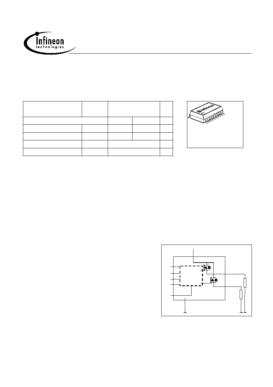
P-DSO-20-1, -6, -7, -9, -14, -15
General Description
∑
N channel vertical power MOSFET with charge pump, ground referenced CMOS compatible input and
diagnostic feedback, monolithically integrated in Smart SIPMOS
technology.
∑
Providing embedded protective functions.
∑
Extern adjustable current limitation.
Application
∑
All types of resistive, inductive and capacitive loads
∑
µC compatible high-side power switch with diagnostic feedback for 12 V grounded loads
∑
Due to the adjustable current limitation best suitable for loads with high inrush currents, so as lamps
∑
Replaces electromechanical relays, fuses and discrete circuits
Basic Functions
∑
Very low standby current
∑
CMOS compatible input
∑
Improved electromagnetic compatibility (EMC)
∑
Stable behaviour at low battery voltage
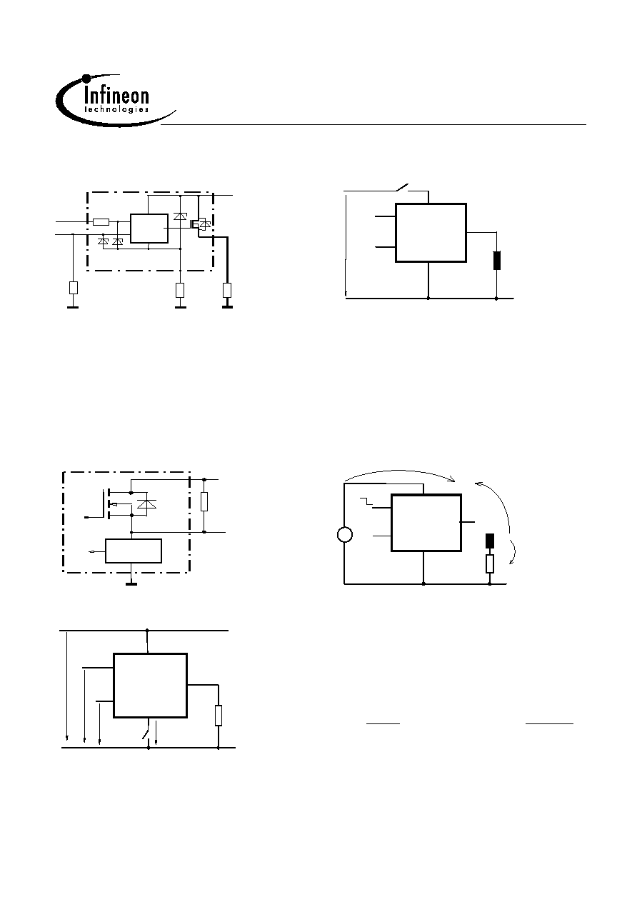
Block Diagram
Vbb
GND
Load 1
Load 2
Logic
Channel 1
Channel 2
IN1
IS1
IN2
IS2
CLA
Protection Functions
∑
Reverse battery protection with external resistor
∑
Short circuit protection
∑
Overload protection
∑
Current limitation
∑
Thermal Shutdown
∑
Overvoltage protection with external resistor
∑
Loss of GND and loss of Vbb protection
∑
Electrostatic discharge Protection (ESD)
Diagnostic Function: IntelliSense
∑
Proportional load current sense ( with defined fault signal during thermal shutdown and overload )
∑
Additional open load detection in OFF - state
∑
Suppressed thermal toggling of fault signal

2004-Mar-08
Page 2
PCN 2004-018-A: BTS 5240G
Functional diagram
OUT1
logic
internal
voltage
supply
ESD
temperature
sensor
clamp for
inductive load
gate control
+
charge
pump
current limit
openload
detection
control and protection circuit
equivalent to
channel 2
IN1
V
bb
GND
IN2
OUT2
LOAD
IS1
IS2
CLA
Channel 1
current
sense
overvoltage
protection
2004-Mar-08
Page 3
PCN 2004-018-A: BTS 5240G
Pin definition and function
Pin
4
7
5
6
3
1,10,
11,15,
16,20
8
17,18,19
12,13,14
2,9
Function
Input 1,2 activates channel1,2 in case of logic high signal
Diagnostic feedback 1 & 2 of channel 1,2
On state: advanced current sense with defined signal in case
of overload or short circuit
Off state: High on failure
Ground of chip
Positive power supply voltage. Design the wiring for the
simultaneous max. short circuit currents from channel 1 to 2 and
also for low thermal resistance
Current limit adjust, the current limit for both channels can be
chosen as high ( potential < 2,6V ) or low ( potential > 3,6V ).
Output 1,2 protected high-side power output of channel 1,2.
Design the wiring for the max. short circuit current.
Not connected
Symbol
IN1
IN2
IS1
IS2
GND 1/2
V
bb
CLA
OUT1
OUT2
N.C.
Pin configuration
V
bb
1
∑
20 V
bb
GND Ω
2
19 OUT1
IN1
3
18 OUT1
IS1
4
17 OUT1
IS2
5
16
IN2
6
15
CLA Ω
7
14 OUT2
8
13 OUT2
N.C. 9
12 OUT2
10
11
V
bb
V
bb
(top view)
V
bb
V
bb
N.C.

2004-Mar-08
Page 4
PCN 2004-018-A: BTS 5240G
Maximum Ratings at T
j
=25∞C, unless otherwise specified
Parameter
Symbol
Value
Unit
Supply voltage (overvoltage protection see page 6)
V
bb
28
1)
V
Supply voltage for full short circuit protection; T
j
= -40...150∞C V
bb(SC)
28
2)
Maximum voltage across DMOS
V
ON
52
Load dump protection
3)
V
LoadDump
4)
= V
A
+ V
S
; V
A
= 13,5 V
In = low or high; t
d
= 400 ms; R
I
4)
= 2
R
L
= 2.25
R
L
= 6.8
V
Loaddump
40
53
Load current (Short - circuit current, see page 7)
I
L
I
L(lim)
5)
A
Operating temperature range
T
j
-40...+150 ∞C
Storage temperature range
T
stg
-55...+150
Dynamical temperature rise at switching
dT
60
K
Power dissipation
6)
(DC), one channel active T
A
= 85 ∞C
P
tot
1,4
W
Maximal switchable inductance, single pulse
V
bb
=12V, T
jstart
=150∞C;
(see diagrams on page 12)
I
L
= 6 A, E
AS
= 0.319 J, R
L
= 0
, one channel:
I
L
= 12 A, E
AS
= 0.679 J, R
L
= 0
, two parallel channels:
Z
L(s)
9.8
5.2
mH
Electrostatic discharge voltage IN:
(Human Body Model)
IS:
according to ANSI EOS/ESD - S5.1 - 1993 , ESD STM5.1 - 1998
OUT:
V
ESD
1.0
2.0
4.0
kV
Continuous input voltage
V
IN
-10...16
V
Voltage at current limit adjustment pin
V
CLA
-10...16
Current limit adjustment current
I
CLA
±
5.0
mA
Current through input pin (DC)
I
IN
±
5.0
Current through sense (DC)
(see page 11)
I
IS
-5...10
118...28 V for 100 hours
2only single pulse, RL = 200 m
; L = 8 µH ; R and L are describing the complete circuit impedance including
line, contact and generator impedances.
3Supply voltage higher than Vbb(AZ) require an external current limit for the GND (150
resistor) and sense pin.
4RI = internal resistance of the load dump test pulse generator.
5
Current limit is a protection function. Operation in current limitation is considered as "outside" normal operating
range. Protection functions are not designed for continuous repetitive operation.
6Device on 50mm*50mm*1.5mm epoxy PCB FR4 with 6 cm2 (one layer, 70µm thick) copper area for Vbb
connection. PCB is vertical without blown air.

2004-Mar-08
Page 5
PCN 2004-018-A: BTS 5240G
Electrical Characteristics
Parameter and Conditions,
each of the two channels
Symbol
Values
Unit
at T
j
= -40...+150 ∞C, V
bb
= 9...16 V,
unless otherwise specified
min.
typ.
max.
Thermal Resistance
junction - soldering point each channel:
R
thJS
-
18
-
K/W
junction - ambient
1)
one channel active:
all channels active:
R
thJA
-
44
42
-
K/W
Load Switching Capabilities and Characteristics
On-state resistance (V
bb
to OUT),
(see page 13)
T
j
= 25 ∞C, I
L
= 5 A, each channel:
T
j
= 150 ∞C, each channel:
T
j
= 25 ∞C, two parallel channels:
R
ON
-
-
-
21
42
11
25
50
13
m
Nominal load current
1)
T
a
= 85∞C, T
j
150∞C , one channel active:
two channels active, per channel:
I
L(nom)
5.4
3.9
5.9
4.2
-
-
A
Output voltage drop limitation at small load currents
I
L
= 0.5 A
V
ON(NL)
-
40
-
mV
Output current while GND disconnected
2)
( see diagram page 12 )
V
IN
= 0 V
I
L(GND
high
)
-
-
2
mA
1Device on 50mm*50mm*1.5mm epoxy PCB FR4 with 6 cm2 (one layer, 70µm thick) copper area for Vbb
connection. PCB is vertical without blown air.
2not subject to production test, specified by design

2004-Mar-08
Page 6
PCN 2004-018-A: BTS 5240G
Electrical Characteristics
Parameter and Conditions,
each of the two channels
Symbol
Values
Unit
at T
j
= -40...+150 ∞C, V
bb
= 9...16 V,
unless otherwise specified
min.
typ.
max.
Load Switching Capabilities and Characteristics
Turn-on time
1)
to 90%
V
OUT
R
L
= 12
, V
bb
= 12 V
t
on
-
90
200
µs
Turn-off time
1)
to 10%
V
OUT
R
L
= 12
, V
bb
= 12 V
t
off
-
100
220
Slew rate on
1)
10 to 30% V
OUT
,
R
L
= 12
, V
bb
= 12 V
dV/dt
on
0.1
0.25
0.45 V/µs
Slew rate off
1)
70 to 40% V
OUT
,
R
L
= 12
, V
bb
= 12 V
-dV/dt
off
0.09
0.25
0.4
Operating Parameters
Operating voltage
2)
V
bb(on)
4.5
-
28
V
Overvoltage protection
3)
I
bb
= 40 mA
V
bb(AZ)
41
47
52
Standby current
4)
(see diagram on page 13)
T
j
= -40...+25 ∞C, V
IN
= 0 V
T
j
= 150 ∞C
I
bb(off)
-
-
5
-
7.5
20
µA
1See timing diagram on page 14.
218V...28V for 100 hours
3Supply voltages higher than Vbb(AZ) require an external current limit for the status pin and GND pin (e.g. 150
).
See also VOut(CL) in table of protection functions and circuit diagram on page 11.
4Measured with load; for the whole device; all channels off.

2004-Mar-08
Page 7
PCN 2004-018-A: BTS 5240G
Electrical Characteristics
Parameter and Conditions,
each of the two channels
Symbol
Values
Unit
at T
j
= -40...+150 ∞C, V
bb
= 9...16 V,
unless otherwise specified
min.
typ.
max.
Operating Parameters
Off-State output current (included in
I
bb(off)
)
V
IN
= 0 V, each channel
I
L(off)
-
1.5
8
µA
Operating current
1)
V
IN
= 5 V, per active channel
I
GND
-
1.6
4
mA
Protection Functions
2)
Current limit,
( see timing diagrams, page 15 )
Low level;
if potential at CLA = high
High level;
if potential at CLA = low
I
L(LIM)
7
40
11
50
14
60
A
Current limit adjustment threshold voltage
V
CLA(T-)
V
CLA(T+)
2.
0
-
-
-
-
4.0
V
Repetitive short circuit current limit
T
j
= T
jt
(see timing diagrams on page 15)
High level one active channel:
two active channels
3)
:
Low level one active channel:
two active channels
3)
:
I
L(SCr)
-
-
-
-
40
40
7
7
-
-
-
-
A
Initial short circuit shutdown time low level:
T
j,start
= 25∞C ; V
bb
= 13,5 V
high level:
t
off(SC)
-
-
3.5
0.75
-
-
ms
Output clamp (inductive load switch off)
4)
I
L
= 40 mA
V
OUT(CL)
-
-15
-
V
Thermal overload trip temperature
T
jt
150
170
-
∞C
Thermal hysteresis
T
jt
-
10
-
K
1Add IIS, if IIS > 0
2Integrated protection functions are designed to prevent IC destruction under fault conditions
described in the data sheet. Fault conditions are considered as "outside" normal operating range.
Protection functions are not designed for continuous repetitive operation.
3At the beginning of the short circuit the double current is possible for a short time.
4If channels are connected in parallel, output clamp is usually accomplished by the
channel with the lowest VOUT(CL).

2004-Mar-08
Page 8
PCN 2004-018-A: BTS 5240G
Electrical Characteristics
Parameter and Conditions,
each of the two channels
Symbol
Values
Unit
at T
j
= -40...+150 ∞C, V
bb
= 9...16 V,
unless otherwise specified
min.
typ.
max.
Diagnostic Characteristics
Open load detection voltage
V
OUT(OL)
2
3.2
4.4
V
Internal output pull down
1)
V
OUT
= 13.5 V
R
OUT(PD)
11
23
35
k
Current sense ratio, static on-condition
k
ILIS
= I
L
:I
IS
I
L
= 0.5 A
I
L
= 3 A
I
L
= 6 A
k
ILIS
4640
4900
4900
5800
5400
5350
6960
5900
5800
Sense signal in case of fault-conditions
2)
in off-state
V
fault
5
6.2
7.5
V
Current saturation of sense fault signal
I
fault
4
-
-
mA
Sense signal delay after thermal shutdown
3)
t
delay(fault)
-
-
1.2
ms
Current sense output voltage limitation
I
IS
= 0 , I
L
= 5 A
V
IS(lim)
5.4
6.5
7.3
V
Current sense leakage/offset current
V
IN
= 5 V, I
L
= 0 , V
IS
= 0
I
IS(LH)
-
-
5
µA
Current sense settling time to I
IS
static
±
10%
after positive input slope
4)
, I
L
= 0 to 5A
t
son(IS)
-
-
400
µs
Current sense settling time to I
IS
static
±
10%
after change of load current
4)
, I
L
= 2.5 to 5A
t
slc(IS)
-
-
300
1In case of floating output, the status doesn¥t show open load.
2Fault condition means output voltage exceeds open load detection voltage VOUT(OL)
3In the case of thermal shutdown the Vfault signal remains for tdelay(fault) longer
than the restart of the switch ( see diagram on page 16 ).
4not subject to production test, specified by design

2004-Mar-08
Page 9
PCN 2004-018-A: BTS 5240G
Electrical Characteristics
Parameter
Symbol
Values
Unit
at T
j
= -40...+150 ∞C, V
bb
= 9...16 V,
unless otherwise specified
min.
typ.
max.
Diagnostic Characteristics
Status invalid after negative input slope
t
d(SToff)
-
-
1.2
ms
Status invalid after positive input slope
with open load
t
d(STOL)
-
-
20
µs
Input Feedback
1)
Input resistance
(see circuit page 11)
R
I
2.0
3.5
5.5
k
Input turn-on threshold voltage
V
IN(T+)
-
-
2.4
V
Input turn-off threshold voltage
V
IN(T-)
1.0
-
-
Input threshold hysteresis
V
IN(T)
-
0.5
-
Off state input current
V
IN
= 0.4 V
I
IN(off)
3
-
40
µA
On state input current
V
IN
= 5 V
I
IN(on)
20
50
90
Reverse Battery
2)
Reverse battery
-V
bb
-
-
27
V
Drain-source diode voltage (V
OUT
> V
bb
)
T
j
= 150 ∞C, I
bb
= -10 mA
-V
ON
-
330
-
mV
1If ground resistors RGND are used, add the voltage drop across these resistor.
2Requires a 150
resistor in GND connection. The reverse load current through the intrinsic drain-source diode
has to be limited by the connected load. Power dissipation is higher compared to normal operating conditions
due to the voltage drop across the drain-source diode. The temperature protection is not active during reverse
current operation! Input and status currents have to be limited. (see max. ratings page 4)
2004-Mar-08
Page 10
PCN 2004-018-A: BTS 5240G
Truth Table - for each of the two channels
Input
level
Output
level
Diagnostic
output
Normal
Operation
L
H
L
V
bb
Z
1)
I
IS
= I
L
/ kilis
Current
Limitation
2)
H
V
bb
V
fault
Short circuit
to GND
L
H
L
L
Z
1)
V
fault
Overtemperature
L
H
L
L
Z
1)
V
fault
Short circuit
to V
bb
L
H
V
bb
V
bb
V
fault
< I
IS
= I
L
/ kilis
3)
Open load
L
H
>V
out(OL)
V
bb
V
fault
Z
1)
L
= " Low" Level Z = high impedance, potential depends on external circuit
H = "High" Level V
fault
= 5V typ., constant voltage independent of external sense resistor.
Parallel switching of channels is possible by connecting the inputs and outputs parallel.
The current sense ouputs have to be connected with a single sense resistor.
Terms
PROFET
IN2
OUT2
GND
Vbb
V
OUT2
I
GND
VON2
18
3
15,16,20
4
5
IN1
V
OUT1
VON1
I L1
OUT1
7
12
VIN1 VIN2 I IS2
Ibb
I IN1
I IN2
I IS1
I L2
V
bb
V
IS2
6
1,10,11
V
IS1
8
V
CLA
IS1
IS2
CLA
13
14
19
17
Leadframe ( Vbb ) is connected to pin 1,10,11,15,16,20
1L-potential by using a sense resistor
2Current limitation is only possible while the device is switched on.
3Low ohmic short to Vbb may reduce the output current IL and therefore also the sense current IIS.
2004-Mar-08
Page 11
PCN 2004-018-A: BTS 5240G
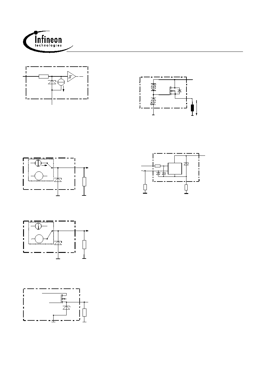
Input circuit ( ESD protection ), IN1 or IN2
IN
GND
I
R
ESD-ZD
I
I
I
The use of ESD zener diodes as voltage clamp
at DC conditions is not recommended.
Inductive and overvoltage output clamp,
OUT1 or OUT2
Sense-Status output, IS1 or IS2
ON-State: Normal operation: IS = IL / kILIS
VIS = IS * RIS; RIS = 1k
nominal
RIS > 500
IS
GND
IS
R
IS
I
ESD-ZD
IS
V
V
f
Sense output
logic
+Vbb
OUT
V
OUT
Power GND
GND
V
Z
+Vbb
OUT
V
OUT
Power GND
GND
V
Z
ESD zener diode: V
ESD
= 6,1 V typ., max. 14 mA ;
ON-State: Fault condition so as thermal shut down
or current limitation
VOUT clamped to VOUT(CL) = -15 V typ.
Overvolt. Protection of logic part
OUT1 or OUT2
GND
IS
R
ESD-ZD
V
fault
V
fault
V
f
Sense output
logic
+ V bb
IN
IS
IS
R
GN D
GN D
R
Signal GN D
Logic
PR OFET
V
Z2
I
R
V
Z1
Vfault = 6 V typ ; V
fault
< V
ESD
under all conditions
OFF-State diagnostic condition:
Open Load, if V
OUT
> 3 V typ.; IN low
VZ1 = 6,1V typ., VZ2 = 47V typ., RGND = 150
,
RIS = 1k
, RI = 3,5k
typ.
IS - ST
GND
ESD-
ZD
R
IS
Int. 5V
ESD-Zener diode: 6,1V typ., max. 5mA; R
ST(ON)
< 375
at 1,6mA.. The use of ESD zener diodes as voltage clamp
at DC conditions is not recommended.
2004-Mar-08
Page 12
PCN 2004-018-A: BTS 5240G
Reverse battery protection
OUT1 or OUT2
Vbb disconnect with energized inductive
load
- V bb
IN
IS
S ig n a l G N D
L o g ic
P R O F E T
V
Z 2
I
R
V Z1
L o a d G N D
G N D
R
O U T
IS
R
L o a d
R
G N D
-I
PROFET
V
IN
IS
OUT
GND
bb
V
bb
high
PROFET
V
IN
IS
OUT
GND
bb
V
bb
V
bb
high
VZ1 = 6,1V typ., VZ2 = 47V typ., RGND = 150
RIS = 1k
, RI = 3,5k
typ.
In case of reverse battery the load current has to
be limited by the load. Protection functions are
not active.
For inductive load currents up to the limits defined
by ZL each switch is protected against loss of Vbb.
(max. ratings and diagram on page 12)
Consider at your PCB layout that in the case of Vbb
disconnection with energized inductive load all the
load current flows through the GND connection.
Open load detection, OUT1 or 2
Off-state diagnostic condition:
Open load, if VOUT > 3 V typ.; IN = low
Inductive load switch-off energy
dissipation
O p en lo ad
d etectio n
Logic
unit
V OU T
S ig na l G N D
O F F
R E XT
V bb
PROFET
V
IN
IS
OUT
GND
bb
=
E
E
E
EAS
bb
L
R
ELoad
RL
L
{
L
Z
GND disconnect
Energy stored in load inductance: E
L
= Ω * L * I
L
2
While demagnetizing load inductance,
the enÈrgy dissipated in PROFET is
E
AS
= E
bb
+ E
L
- E
R
=
V
ON(CL)
* i
L
(t) dt,
with an approximate solution for R
L
> 0
:
PROFET
V
IN
IS
OUT
GND
bb
V
bb
V
IN
V
IS
VGND
E
I
L
R
V
V
I
R
V
AS
L
L
bb
OUT CL
L
L
OUT CL
=
+
+
*
*
*(
|
)* ln(
*
|
|
)
(
)|
(
)
2
1
Any kind of load.

2004-Mar-08
Page 13
PCN 2004-018-A: BTS 5240G
Typ. standby current
I
bb(off)
= f(T
j
) ; V
bb
= 16 V ; V
IN1,2
= low
Maximum allowable load inductance
for a single switch off (one channel)
L =f(I
L
); T
jstart
= 150∞C, V
bb
= 12V, R
L
= 0
0
2
4
6
8
10
12
14
16
-40 -20 0
20 40 60 80 100 120 140 160
T
j
[∞C]
I
bb(
of
f
)
[µ
A
]
0,1
1
10
100
1000
0
5
10
15
20
I
L
[A]
Z
L(
s
)
[m
H
]
Typ. on-state resistance
R
ON
= f(V
bb
,T
j
); I
L
= 5 A ; V
in
= high
12
14
16
18
20
22
24
26
28
30
0
5
10
15
20
25
30
35
V
bb
[V]
R
on
[m
O
h
m
]
2004-Mar-08
Page 14
PCN 2004-018-A: BTS 5240G
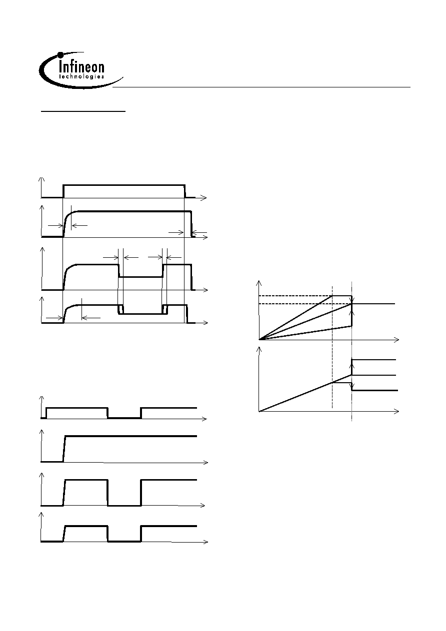
Timing diagrams
All channels are symmetric and consequently the diagrams are valid for channel 1 and channel 2.
Figure 1c: Behaviour of sense output:
Sense current (I
S
) and sense voltage (V
S
)
as function of load current dependent on
the sense resistor.
Shown is V
S
and I
S
for three different
sense resistors. Curve 1 refers to a low
resistor, curve 2 to a medium-sized
resistor and curve 3 to a big resistor.
Note, that the sense resistor may not falls
short of a minimum value of 500
.
Figure 1a: Switching a resistive load,
change of load current in on-condition
IN
OUT
L
t
V
I
I
S
,V
S
t
son(IS)
t
t
slc(IS)
slc(IS)
Load 1
Load 2
t
t
on
off
V
S
I
L(lim)
V
fault
V
ESD
I
S
I
L
I
L
1
2
1
3
2
3
The sense signal is not valid during settling time after
turn on or change of load current. tslc(IS) = 300 µs typ.
Figure 1b: V
bb
turn on
IN
V
L
I
bb
I
S
,V
S
I
S
= I
L
/ k
ILIS
V
IS
= I
S
* R
IS
; R
IS
= 1k
nominal
R
IS
> 500
proper turn on under all conditions
2004-Mar-08
Page 15
PCN 2004-018-A: BTS 5240G
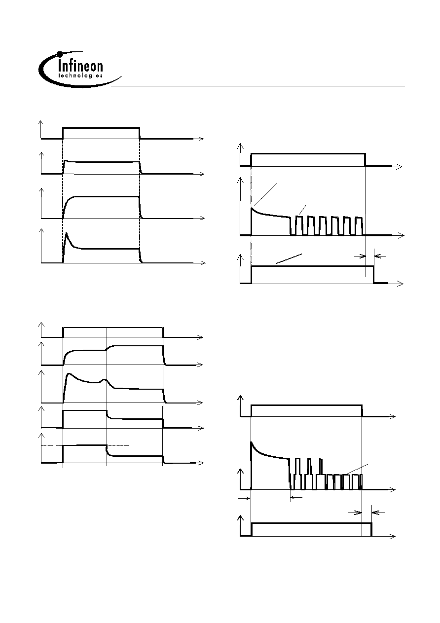
Figure 2a: Switching a lamp
Figure 3a: Short circuit:
Shut down by overtemperature,
reset by cooling
IN
IS
O U T
L
t
V
I
IN
I
IL(lim)
L
V
S
V
fault
L(SCr)
I
t
delay
fault
Figure 2b: Switching a lamp with current limit:
The behaviour of I
S
and V
S
is shown for a
resistor, which refers to curve 1 in figure 1c
Heating up may require several milliseconds,
depending on external conditions.
IL(lim) = 50A typ. increases with
decreasing temperature.
Figure 3a: Turn on into short circuit,
shut down by overtemperature, restart by cooling
( channel 1 and 2 switched parallel )
IN
O U T
L
t
V
I
I
S
V
S
V
fa u lt
IN
O U T
L
t
V
I
I
S
V
S
V
fa u lt
IN 1 /2
L (S C r)
I
2 x IL(lim )
toff(SC)
V
S 1
, V
S 2
V
fau lt
t
d e la y
fa u lt
IL1 + IL2
2 x IL(lim )
2004-Mar-08
Page 16
PCN 2004-018-A: BTS 5240G
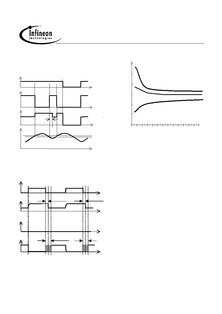
Figure 4a: Overtemperature
Reset if
Tj < Tjt
The behaviour of IS and VS is shown for a resistor,
which refers to curve 1 in figure 1c.
t
IN
IL
T
J
I
S
t
delay(fault)
Figure 5a:Open-load: detection in OFF-state,
turn on/off to open load.
Open load of channel 1; other channels normal
opertaion.
Figure 6b: Current sense ratio
1)
0 1 2 3 4 5 6 7 8 9 10 11 12 13
IL
[A]
kILIS
4000
5000
6000
7000
OUT1
V
IS
IN1
I
L1
t
ST delay
t
off
t
ST delay
off
t
V
fault
toff = 250µs max.; tST delay = 500µs max.
with pull up resistor at output
1This range for the current sense ratio refers to all devices. The accuracy of the kILIS can
be raised by calibrating the value of kILIS for every single device.
2004-Mar-08
Page 17
PCN 2004-018-A: BTS 5240G
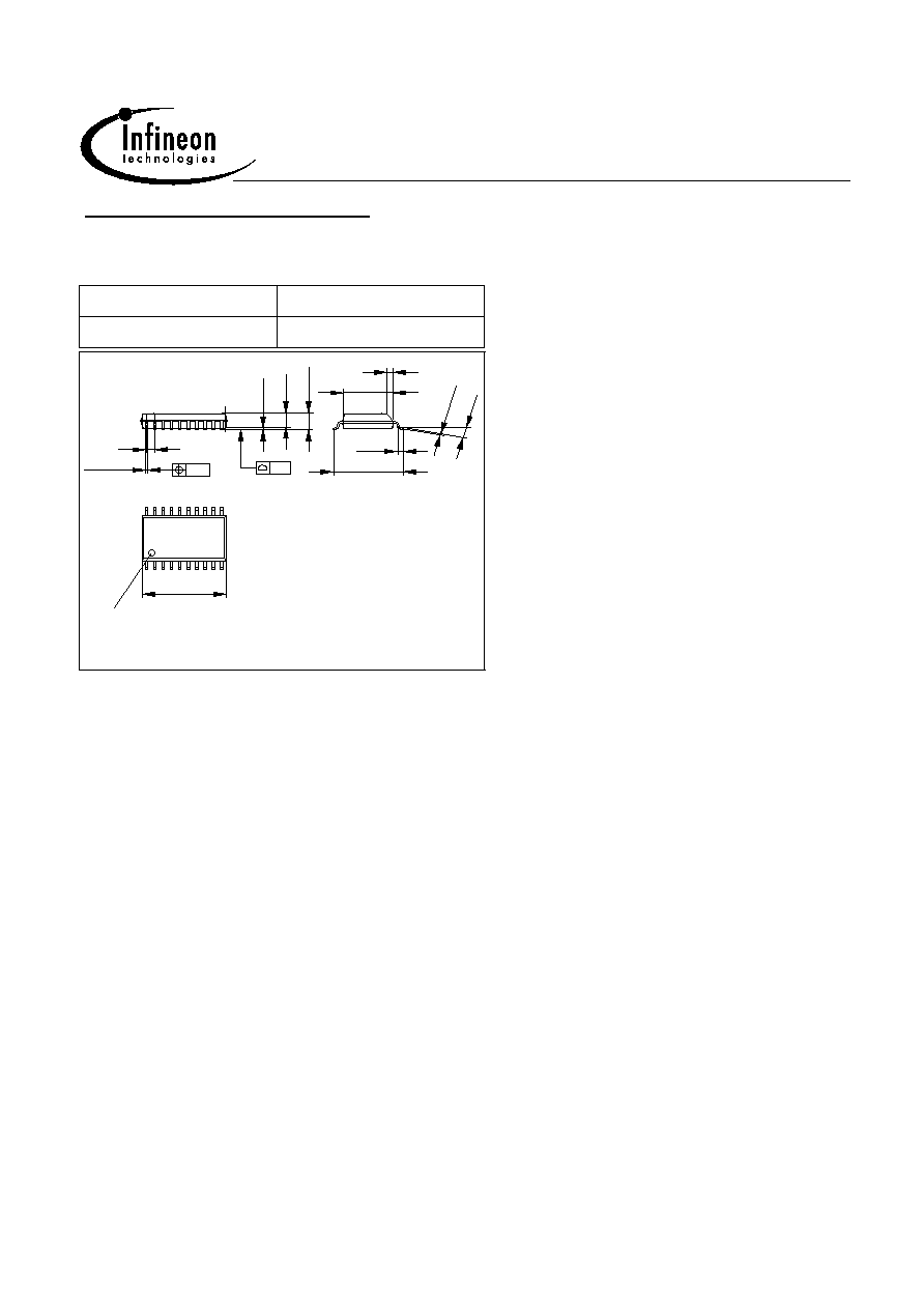
Package and ordering code
all dimensions in mm
Published by
Infineon Technologies AG,
St.-Martin-Strasse 53,
D-81669 M¸nchen
© Infineon Technologies AG 2001
All Rights Reserved.
Attention please!
The information herein is given to describe certain
components and shall not be considered as
a guarantee of characteristics.
Terms of delivery and rights to technical change
reserved.
We hereby disclaim any and all warranties, including
but not limited to warranties of non-infringement,
regarding circuits, descriptions and charts stated herein.
Infineon Technologies is an approved CECC
manufacturer.
Information
For further information on technology, delivery
terms and conditions and prices please contact
your nearest Infineon Technologies Office in
Germany or our Infineon Technologies
Representatives worldwide (see address list).
Warnings
Due to technical requirements components may
contain dangerous substances. For information
on the types in question please contact your
nearest Infineon Technologies Office.
Infineon Technologies Components may only be
used in life-support devices or systems with the
express written approval of Infineon Technologies,
if a failure of such components can reasonably be
expected to cause the failure of that life-support
device or system, or to affect the safety or
effectiveness of that device or system. Life support
devices or systems are intended to be implanted in
the human body, or to support and/or maintain and
sustain and/or protect human life. If they fail, it is
reasonable to assume that the health of the user or
other persons may be endangered.
P-DSO-20-21
Sales Code
BTS 5240G
Ordering Code
Q67060-S6145
1
10
11
20
Index Marking
1) Does not include plastic or metal protrusions of 0.15 max per side
2) Does not include dambar protrusion of 0.05 max per side
GPS05094
2.65 max
0.1
0.2
-0.1
2.45
-0.2
+0.15
0.35
1.27
2)
0.2 24x
-0.2
7.6
1)
0.35 x 45∞
0.23
8∞ max
+0.09
+0.8
±0.3
10.3
0.4
12.8
-0.2
1)