 | –≠–ª–µ–∫—Ç—Ä–æ–Ω–Ω—ã–π –∫–æ–º–ø–æ–Ω–µ–Ω—Ç: BTS555 | –°–∫–∞—á–∞—Ç—å:  PDF PDF  ZIP ZIP |

PROFETÆ Data Sheet BTS555
Infineon Technologies AG 1 of 16
2003-Oct-01
Smart Highside High Current Power Switch
Reversave
Reversave
∑
Reverse battery protection by self turn on of
power MOSFET
Features
∑
Overload protection
∑
Current limitation
∑
Short circuit protection
∑
Overtemperature protection
∑
Overvoltage protection (including load dump)
∑
Clamp of negative voltage at output
∑
Fast deenergizing of inductive loads
2)
∑
Low ohmic inverse current operation
∑
Diagnostic feedback with load current sense
∑
Open load detection via current sense
∑
Loss of V
bb
protection
3)
∑
Electrostatic discharge (ESD) protection
Application
∑
Power switch with current sense diagnostic
feedback for 12
V and 24
V DC grounded loads
∑
Most suitable for loads with high inrush current
like lamps and motors; all types of resistive and inductive loads
∑
Replaces electromechanical relays, fuses and discrete circuits
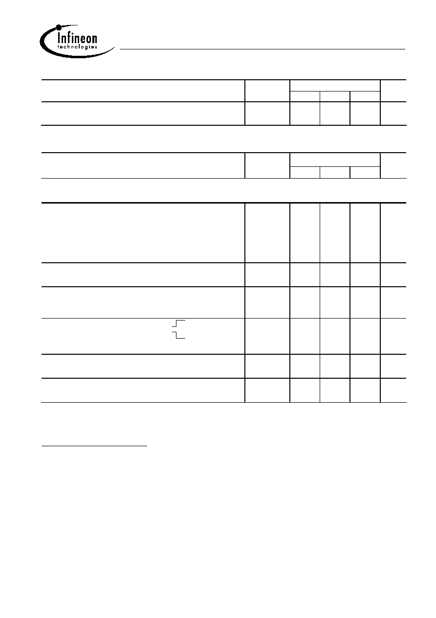
General Description
N channel vertical power FET with charge pump, current controlled input and diagnostic feedback with load
current sense, integrated in Smart SIPMOS
chip on chip technology. Providing embedded protective functions.
IN
Charge pump
Level shifter
Rectifier
Limit for
unclamped
ind. loads
Gate
protection
Current
limit
2
Overvoltage
protection
+ Vbb
PROFET
OUT
3 & Tab
1, 5
Load GND
Load
Output
Voltage
detection
RIS
IS
4
I
IS
I
L
V
IS
I
IN
Logic GND
Voltage
sensor
Voltage
source
Current
Sense
Logic
ESD
Temperature
sensor
R bb
V
IN
1
)
Due to the different lead frame geometry Ron @25∞C is 0.3 m
higher in staggered than in straight version,
and accordingly for other temperatures.
2
)
With additional external diode.
3)
Additional external diode required for energized inductive loads (see page 9).
Product Summary
Overvoltage protection
V
bb(AZ)
62
V
Output clamp
V
ON(CL)
44
V
Operating voltage
V
bb(on)
5.0
...
34
V
On-state resistance
R
ON
1
)
2.5
m
Load current (ISO)
I
L(ISO)
165
A
Short circuit current limitation
I
L(SCp)
520
A
Current sense ratio
I
L :
I
IS
30 000
TO-218AB/5 TO-218AB-5-1
5
1
Straight leads
Staggered leads

Data Sheet BTS555
Infineon Technologies AG
2
2003-Oct-01
Pin Symbol
Function
1 OUT
O
Output to the load. The pins
1 and 5 must be shorted with each other
especially in high current applications!
4
)
2
IN
I
Input, activates the power switch in case of short to ground
3 Vbb
+
Positive power supply voltage, the tab is electrically connected to this pin.
In high current applications the tab should be used for the V
bb
connection
instead of this pin
5
)
.
4 IS
S
Diagnostic feedback providing a sense current proportional to the load
current; zero current on failure (see Truth Table on page 7)
5 OUT
O
Output to the load. The pins
1 and 5 must be shorted with each other
especially in high current applications!
4)
Maximum Ratings at T
j
= 25 ∞C unless otherwise specified
Parameter Symbol
Values
Unit
Supply voltage (overvoltage protection see page 4)
V
bb
40
V
Supply voltage for full short circuit protection,
(E
AS
limitation see diagram on page 9)
T
j,start
=-40 .+150∞C:
V
bb
34
V
Load current (short circuit current, see page 5)
I
L
self-limited
A
Load dump protection V
LoadDump
=
U
A
+
V
s
, U
A
=
13.5
V
R
I
6
)
=
2
, R
L
=
0.1
, t
d
=
200
ms,
IN,
IS
= open or grounded
V
Load dump
7
)
80
V
Operating temperature range
Storage temperature range
T
j
T
stg
-40 ...+150
-55 ...+150
∞C
Power dissipation (DC), T
C
25 ∞C
P
tot
360
W
Inductive load switch-off energy dissipation, single pulse
V
bb
=
12V, T
j,start
=
150∞C, T
C
=
150∞C const.,
I
L
=
20
A, Z
L
=
15
mH, 0
,
see diagrams on page 10
E
AS
3
J
Electrostatic discharge capability (ESD)
Human Body Model acc. MIL-STD883D, method 3015.7 and ESD
assn. std. S5.1-1993, C = 100 pF, R = 1.5 k
V
ESD
4.0
kV
Current through input pin (DC)
Current through current sense status pin (DC)
see internal circuit diagrams on page 7 and 8
I
IN
I
IS
+15
, -250
+15
, -250
mA
4)
Not shorting all outputs will considerably increase the on-state resistance, reduce the peak current capability
and decrease the current sense accuracy
5)
Otherwise add up to 0.5 m
(depending on used length of the pin) to the R
ON
if the pin is used instead of the
tab.
6)
R
I
= internal resistance of the load dump test pulse generator.
7)
V
Load dump
is setup without the DUT connected to the generator per ISO 7637-1 and DIN 40839.
Data Sheet BTS555
Infineon Technologies AG
3
2003-Oct-01
Thermal Characteristics
Parameter and Conditions Symbol
Values
Unit
min typ
max
Thermal resistance
chip - case
:
R
thJC
8
)
-- --
0.35
K/W
junction - ambient (free air):
R
thJA
--
30 --
Electrical Characteristics
Parameter and Conditions Symbol
Values
Unit
at T
j
=
-40 ... +150
∞C, V
bb
=
12
V unless otherwise specified
min typ
max
Load Switching Capabilities and Characteristics
On-state resistance
(Tab to pins 1,5, see measurement
circuit page 7)
I
L
=
30
A, T
j
=
25
∞C:
V
IN
=
0, I
L
=
30
A
,
T
j
=
150
∞C:
R
ON
1)
--
--
1.9
3.3
2.5
4.0
m
I
L
=
120
A
,
T
j
=
150
∞C:
--
--
4.0
V
bb
=
6 V
9
)
, I
L
=
20
A
,
T
j
=
150
∞C: R
ON(Static)
1)
-- 4.6 9.0
Nominal load current
10
)
(Tab to pins 1,5)
ISO 10483-1/6.7: V
ON
=
0.5
V, Tc =
85
∞C
11
)
I
L(ISO)
128
165
--
A
Maximum load current in resistive range
(Tab to pins 1,5)
V
ON
=
1.8
V, Tc =
25
∞C:
see diagram on page 13
V
ON
=
1.8
V, Tc =
150
∞C:
I
L(Max)
520
360
--
--
--
--
A
Turn-on time
12
)
IIN
to 90% V
OUT
:
Turn-off time
IIN
to 10% V
OUT
:
R
L
=
1
,
T
j
=-40...+150∞C
t
on
t
off
120
50
--
--
600
200
µ
s
Slew rate on
12)
(10 to 30% V
OUT
)
R
L
=
1
dV/dt
on
0.3 0.5 0.8
V/
µ
s
Slew rate off
12)
(70 to 40% V
OUT
)
R
L
=
1
-dV/dt
off
0.3
0.7 1
V/
µ
s
8)
Thermal resistance R
thCH
case to heatsink (about 0.25 K/W with silicone paste) not included!
9
) Decrease of V
bb
below 10 V causes slowly a dynamic increase of R
ON
to a higher value of R
ON(Static)
. As
long as V
bIN
> V
bIN(u) max
, R
ON
increase is less than 10 % per second for T
J
< 85 ∞C.
10)
not subject to production test, specified by design
11)
T
J
is about 105∞C under these conditions.
12
) See timing diagram on page 14.

Data Sheet BTS555
Infineon Technologies AG
4
2003-Oct-01
Parameter and Conditions Symbol
Values
Unit
at T
j
=
-40 ... +150
∞C, V
bb
=
12
V unless otherwise specified
min typ
max
Inverse Load Current Operation
On-state resistance
(Pins 1,5 to pin 3)
V
bIN
=
12 V, I
L
=
-
30
A
T
j
=
25
∞C:
see diagram on page 10
T
j
=
150
∞C:
R
ON(inv)
1)
--
1.9
3.3
2.5
4.0
m
Nominal inverse load current
(Pins 1,5 to Tab)
V
ON
=
-0.5
V, Tc =
85
∞C
11
I
L(inv)
128
165
--
A
Drain-source diode voltage
(V
out
> V
bb
)
I
L
=
-
20
A, I
IN
= 0, T
j
=
+150∞C
-V
ON
-- 0.6 0.7
V
Operating Parameters
Operating voltage (V
IN
=
0)
13
)
V
bb(on)
5.0
--
34
V
Undervoltage shutdown
14
)
V
bIN(u)
1.5 3.0 4.5
V
Undervoltage start of charge pump
see diagram page
15
V
bIN(ucp)
3.0
4.5 6.0
V
Overvoltage protection
15
)
T
j
=-40∞C:
I
bb
=
15
mA
T
j
=
25...+150∞C:
V
bIN(Z)
60
62
--
66
--
--
V
Standby current
T
j
=-40...+25∞C:
I
IN
=
0
T
j
=
150∞C:
I
bb(off)
--
--
15
25
25
50
µ
A
13
) If the device is turned on before a V
bb
-decrease, the operating voltage range is extended down to V
bIN(u)
.
For the voltage range 0..34 V the device is fully protected against overtemperature and short circuit.
14
) V
bIN
= V
bb
-
V
IN
see diagram on page 7. When V
bIN
increases from less than V
bIN(u)
up to V
bIN(ucp)
= 5
V
(typ.) the charge pump is not active and V
OUT
V
bb
-
3
V.
15)
See also V
ON(CL)
in circuit diagram on page 8.

Data Sheet BTS555
Infineon Technologies AG
5
2003-Oct-01
Parameter and Conditions Symbol
Values
Unit
at T
j
=
-40 ... +150
∞C, V
bb
=
12
V unless otherwise specified
min typ
max
Protection Functions
16
)
Short circuit current limit
(Tab to pins 1,5)
17
)
V
ON
=
12
V, time until shutdown max. 300
µ
s
T
c
=-40∞C:
T
c
=25∞C:
T
c
=+150∞C:
I
L(SCp)
200
200
300
320
400
480
550
620
650
A
Short circuit shutdown delay after input current
positive slope, V
ON
> V
ON(SC)
min. value valid only if input "off-signal" time exceeds 30
µ
s
t
d(SC)
80
-- 300
µ
s
Output clamp
18
)
I
L
= 40 mA:
(inductive load switch off)
-V
OUT(CL)
14
17
20
V
Output clamp (inductive load switch off)
at V
OUT
= V
bb
- V
ON(CL)
(e.g. overvoltage)
I
L
= 40 mA
V
ON(CL)
40
44 47
V
Short circuit shutdown detection voltage
(pin 3 to pins 1,5)
V
ON(SC)
--
6
--
V
Thermal overload trip temperature
T
jt
150 -- --
∞C
Thermal hysteresis
T
jt
-- 10 --
K
Reverse Battery
Reverse battery voltage
19
)
-V
bb
--
--
16
V
On-state resistance
(Pins 1,5 to pin 3)
T
j
=
25
∞C:
V
bb
=
-12V,
V
IN
=
0,
I
L
=
-
30
A,
R
IS
=
1
k
T
j
=
150
∞C:
R
ON(rev)
1)
--
2.3
3.9
3.0
4.7
m
Integrated resistor in V
bb
line T
j
=
25
∞C:
T
j
=
150
∞C:
R
bb
90
105
110
125
135
150
16
) Integrated protection functions are designed to prevent IC destruction under fault conditions described in the
data sheet. Fault conditions are considered as "outside" normal operating range. Protection functions are not
designed for continuous repetitive operation.
17
) Short circuit is a failure mode. The device is not designed to operate continuously into a short circuit by
permanent resetting the short circuit latch function. The lifetime will be reduced under such conditions.
18
) This output clamp can be "switched off" by using an additional diode at the IS-Pin (see page 8). If the diode
is used, V
OUT
is clamped to V
bb
- V
ON(CL)
at inductive load switch off.
19
) The reverse load current through the intrinsic drain-source diode has to be limited by the connected load (as
it is done with all polarity symmetric loads). Note that under off-conditions (I
IN
=
I
IS
=
0) the power transistor
is not activated. This results in raised power dissipation due to the higher voltage drop across the intrinsic
drain-source diode. The temperature protection is not active during reverse current operation! Increasing
reverse battery voltage capability is simply possible as described on page 9.

Data Sheet BTS555
Infineon Technologies AG
6
2003-Oct-01
Parameter and Conditions Symbol
Values
Unit
at T
j
=
-40 ... +150
∞C, V
bb
=
12
V unless otherwise specified
min typ
max
Diagnostic Characteristics
Current sense ratio,
I
L
=
120
A,T
j
=-40∞C:
static on-condition,
T
j
=25∞C:
k
ILIS
=
I
L
:
I
IS
,
T
j
=150∞C:
V
ON
<
1.5
V
20)
,
I
L
=
30
A,T
j
=-40∞C:
V
IS
<V
OUT
-
5 v,
T
j
=25∞C:
V
bIN
>
4.0
V
T
j
=150∞C:
(see diagram on page 10)
I
L
=
16
A,T
j
=-40∞C:
T
j
=25∞C:
T
j
=150∞C:
I
L
=
12
A,T
j
=-40∞C:
T
j
=25∞C:
T
j
=150∞C:
k
ILIS
25 000
26 000
24 000
25 000
25 000
23 000
24 000
24 000
23 000
23 000
23 000
23 000
29 000
28 500
26 500
31 200
30 200
27 200
33 500
31 500
27 500
40 500
40 500
29 000
34 000
32 000
29 000
40 000
35 000
31 500
48 000
40 000
32 000
61 000
45 000
34 000
I
IS
=0 by IIN =0 (e.g. during deenergizing of inductive loads):
Sense current saturation
I
IS,lim
6.5 -- --
mA
Current sense leakage current
I
IN
=
0, V
IS
=
0:
V
IN
=
0, V
IS
=
0, I
L
0:
I
IS(LL)
I
IS(LH)
--
--
--
2
0.5
--
µ
A
Current sense settling time
21
)
t
s(IS)
--
--
500
µ
s
Overvoltage protection
T
j
=-40∞C:
I
bb
=
15
mA
T
j
=
25...+150∞C:
V
bIS(Z)
60
62
--
66
--
--
V
Input
Input and operating current (see diagram page 13)
IN grounded (V
IN
=
0)
I
IN(on)
--
0.8 1.5
mA
Input current for turn-off
22)
I
IN(off)
-- --
40
µ
A
20)
If V
ON
is higher, the sense current is no longer proportional to the load current due to sense current
saturation, see
I
IS,lim
.
21
) not subject to production test, specified by design
22
) We recommend the resistance between IN and GND to be less than 0.5
k
for turn-on and more than
500
k
for turn-off. Consider that when the device is switched off (I
IN
=
0) the voltage between IN and GND
reaches almost V
bb
.
Data Sheet BTS555
Infineon Technologies AG
7
2003-Oct-01
Truth Table
Input
current
Output Current
Sense
Remark
level
level IIS
Normal
operation
L
H
L
H
0
nominal
=I
L
/ k
ilis
, up to I
IS
=I
IS,lim
Very high
load current
H H I
IS, lim
up to V
ON
=V
ON(Fold back)
I
IS
no longer proportional to I
L
Current-
limitation
H H
0
V
ON
> V
ON(Fold back)
if V
ON
>V
ON(SC)
, shutdown will occure
Short circuit to
GND
L
H
L
L
0
0
Over-
temperature
L
H
L
L
0
0
Short circuit to
V
bb
L
H
H
H
0
<nominal
23)
Open load
L
H
Z
24)
H
0
0
Negative output
voltage clamp
L L
0
Inverse load
current
L
H
H
H
0
0
L = "Low" Level
H = "High" Level
Overtemperature reset via input: I
IN
=low and Tj < Tjt (see diagram on page14)
Short circuit to GND: Shutdown remains latched until next reset via input (see diagram on page 14)
23
) Low ohmic short to V
bb
may reduce the output current I
L
and can thus be detected via the sense current I
IS
.
24
) Power Transistor "OFF", potential defined by external impedance.
Terms
PROFET
V
IN
IS
OUT
bb
V
IN
I
IS
I
IN
V
bb
Ibb
IL
V
OUT
V
ON
2
4
3
1,5
R
IS
V
IS
V
bIN
R
IN
D
S
V
bIS
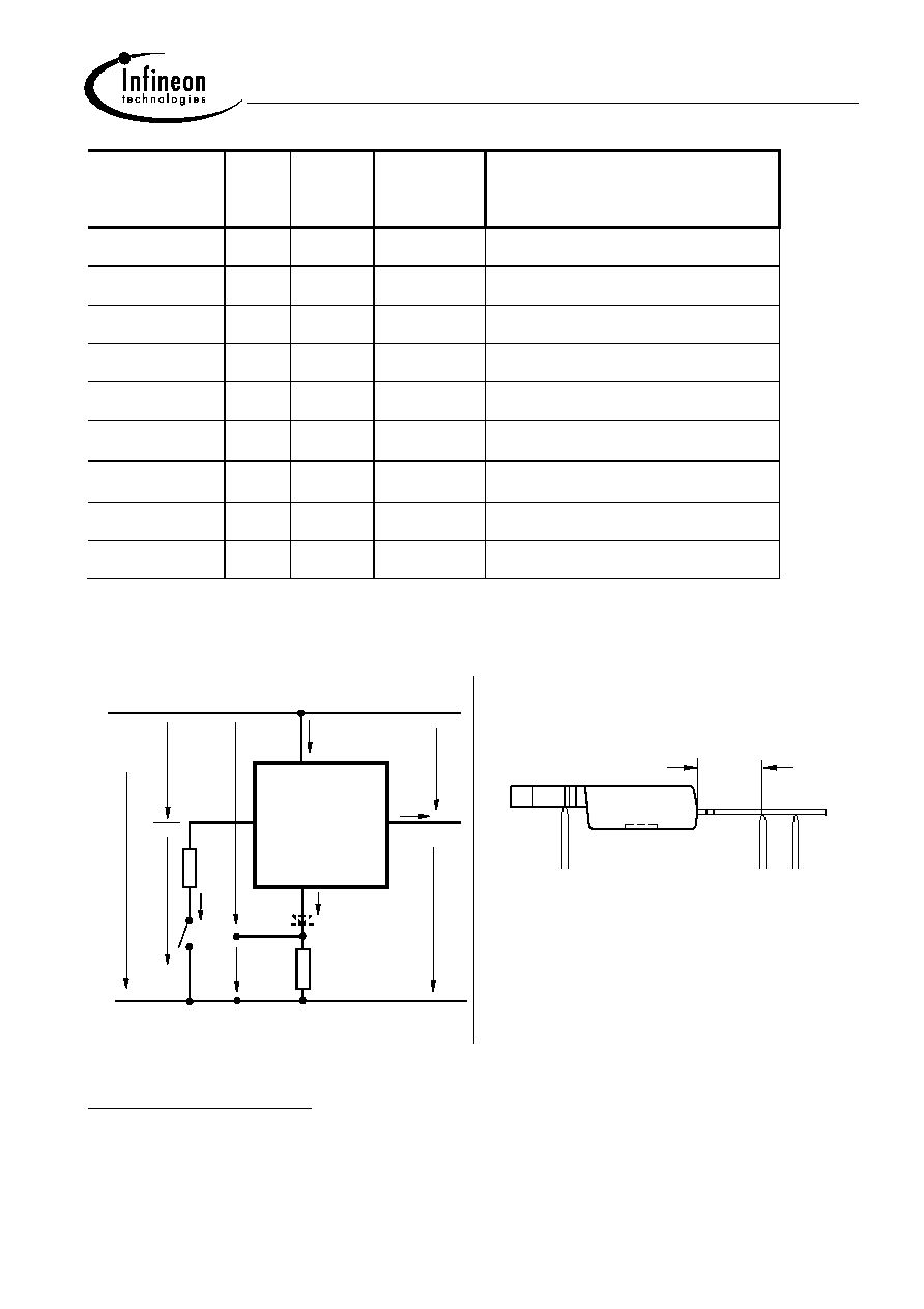
Two or more devices can easily be connected in
parallel to increase load current capability.
R
ON
measurement layout (straight leads)
Sense
V force contacts
Out Force
bb
contacts
5.5 mm
contacts
(both out
pins parallel)
Data Sheet BTS555
Infineon Technologies AG
8
2003-Oct-01
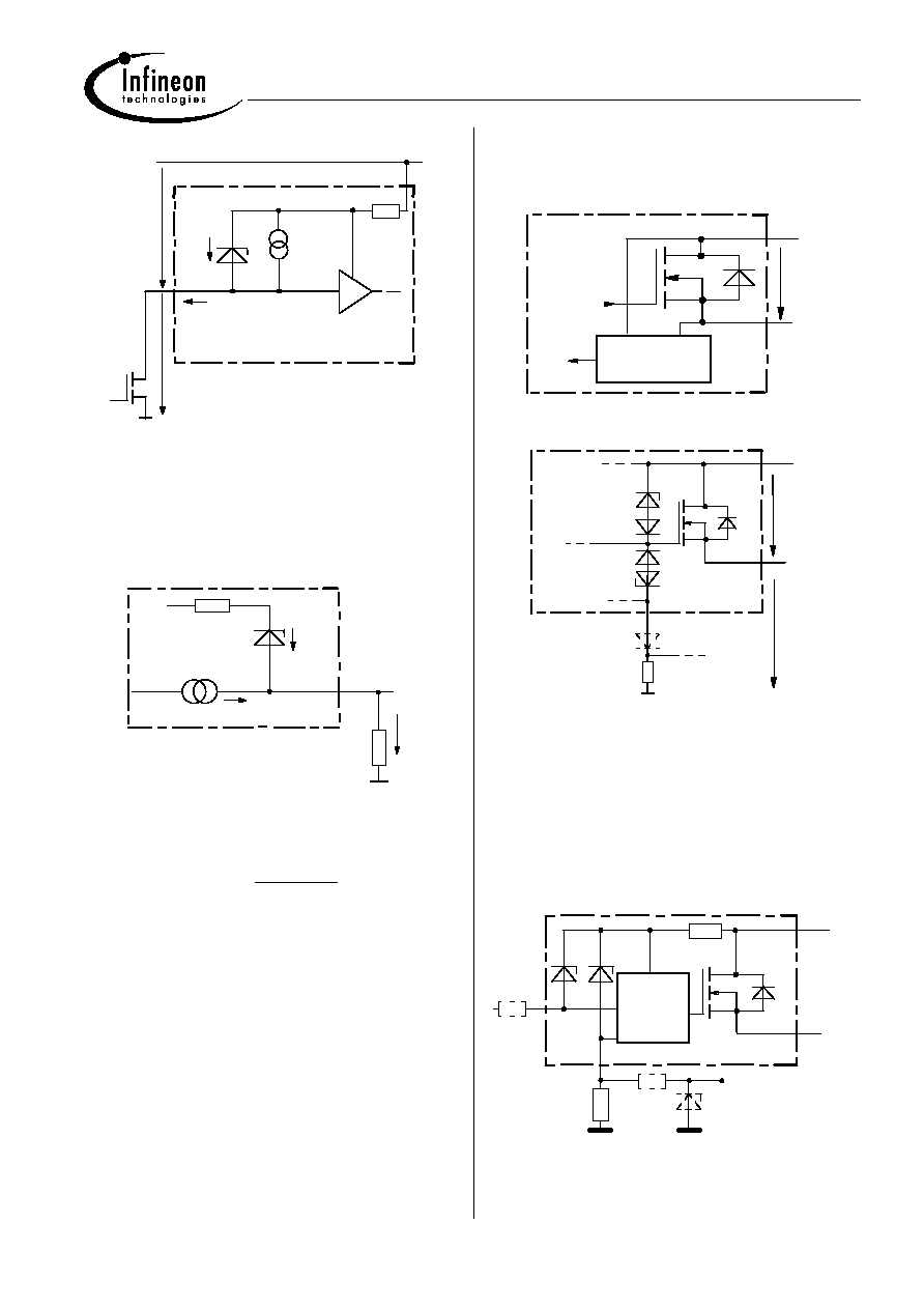
Input circuit (ESD protection)
IN
ZD
IN
I
V bb
Rbb
V
Z,IN
V bIN
V IN
When the device is switched off (I
IN
=
0) the voltage
between IN and GND reaches almost V
bb
. Use a
mechanical switch, a bipolar or MOS transistor with
appropriate breakdown voltage as driver.
V
Z,IN
=
66
V
(typ).
Current sense status output
IS
IS
R
IS
I
ZD
IS
V
bb
V
bb
R
Z,IS
V
V
Z,IS
=
66
V
(typ.), R
IS
=
1
k
nominal (or 1
k
/n, if n
devices are connected in parallel). I
S
= I
L
/k
ilis
can be
only driven by the internal circuit as long as V
out
- V
IS
>
5V. If you want to measure load currents up to I
L(M)
,
R
IS
should be less than
ilis
M
L
bb
K
I
V
V
/
5
)
(
-
.
Note: For large values of R
IS
the voltage V
IS
can reach
almost V
bb
. See also overvoltage protection.
If you don't use the current sense output in your
application, you can leave it open.
Short circuit detection
Fault Condition: V
ON
> V
ON(SC)
(6
V typ.) and t> t
d(SC)
(80 ...300 µs).
Short circuit
detection
Logic
unit
+ Vbb
OUT
V
ON
Inductive and overvoltage output clamp
+ V
bb
OUT
PROFET
V
Z1
V
ON
D
S
IS
V
OUT
V
ZG
V
ON
is clamped to V
ON(Cl)
=
42
V typ. At inductive load
switch-off without D
S
, V
OUT
is clamped to V
OUT(CL)
=
-17
V typ. via V
ZG
. With D
S
, V
OUT
is clamped to V
bb
-
V
ON(CL)
via V
Z1
. Using D
S
gives faster deenergizing of
the inductive load, but higher peak power dissipation in
the PROFET. In case of a floating ground with a
potential higher than 19V referring to the OUT ≠
potential the device will switch on, if diode DS is not
used.
Overvoltage protection of logic part
+ V
bb
V
OUT
IN
bb
R
Signal GND
Logic
PROFET
V
Z,IS
R
IS
IN
R
IS
V
Z,IN
R
V
V
Z,VIS
R
bb
=
120
typ
.
,
V
Z,IN
= V
Z,IS
=
66
V
typ.,
R
IS
=
1
k
nominal. Note that when overvoltage exceeds 71
V
typ.
a voltage above 5V can occur between IS and GND, if
R
V
, V
Z,VIS
are not used.

Data Sheet BTS555
Infineon Technologies AG
9
2003-Oct-01
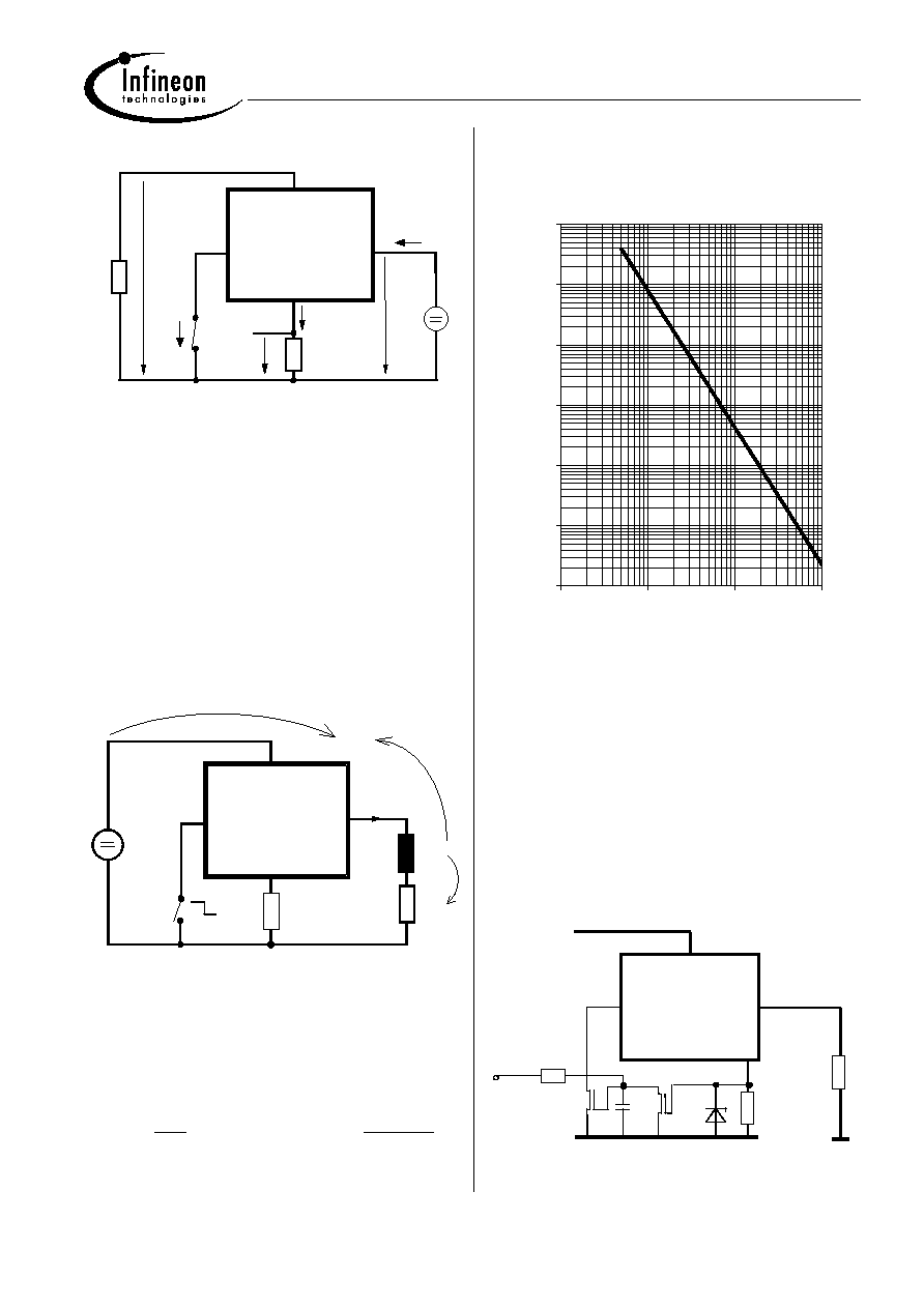
Reverse battery protection
Logic
IS
IN
IS
R
V
R
OUT
L
R
Power GND
Signal GND
Vbb
-
Power
Transistor
IN
R
bb
R
D
S
D
R
V
1
k
,
R
IS
=
1
k
nominal. Add
R
IN
for reverse
battery protection in applications with
V
bb
above
16
V
19)
; recommended value:
1
R
IN
+
1
R
IS
+
1
R
V
=
0.1A
|V
bb
| - 12V
if D
S
is not used (or
1
R
IN
=
0.1A
|V
bb
| - 12V
if D
S
is
used).
To minimize power dissipation at reverse battery
operation, the summarized current into the IN and IS
pin should be about 120mA. The current can be
provided by using a small signal diode D in parallel to
the input switch, by using a MOSFET input switch or by
proper adjusting the current through R
IS
and
R
V
.
V
bb
disconnect with energized inductive
load
Provide a current path with load current capability by
using a diode, a Z-diode, or a varistor. (V
ZL
<
72 V or
V
Zb
<
30 V if R
IN
=0). For higher clamp voltages
currents at IN and IS have to be limited to
250 mA.
Version a:
PROFET
V
IN
OUT
IS
bb
V
bb
V
ZL
Version b:
PROFET
V
IN
OUT
IS
bb
V
bb
V
Zb
Note that there is no reverse battery protection when
using a diode without additional Z-diode V
ZL
, V
Zb
.
Version c: Sometimes a neccessary voltage clamp is
given by non inductive loads R
L
connected to the same
switch and eliminates the need of clamping circuit:
PROFET
V
IN
OUT
IS
bb
V
bb
R
L
Data Sheet BTS555
Infineon Technologies AG
10
2003-Oct-01
Inverse load current operation
PROFET
V
IN
OUT
IS
bb
V
bb
V
OUT
- I
L
R
IS
V
IS
V
IN
+
-
+
-
I
IS
The device is specified for inverse load current
operation (V
OUT
> V
bb
> 0V). The current sense feature
is not available during this kind of operation (I
IS
= 0).
With I
IN
= 0 (e.g. input open) only the intrinsic drain
source diode is conducting resulting in considerably
increased power dissipation. If the device is switched
on (V
IN
= 0), this power dissipation is decreased to the
much lower value R
ON(INV)
* I
2
(specifications see page
4).
Note: Temperature protection during inverse load
current operation is not possible!
Inductive load switch-off energy
dissipation
PROFET
V
IN
OUT
IS
bb
E
E
E
EAS
bb
L
R
ELoad
L
RL
{
Z L
RIS
I
IN
Vbb
i (t)
L
Energy stored in load inductance:
E
L
=
1/2
∑
L
∑
I
2
L
While demagnetizing load inductance, the energy
dissipated in PROFET is
E
AS
= E
bb
+ E
L
- E
R
=
V
ON(CL)
∑
i
L
(t) dt,
with an approximate solution for RL
>
0
:
E
AS
=
I
L
∑
L
2
∑
R
L
(
V
bb
+
|V
OUT(CL)
|)
ln
(1+
I
L
∑
R
L
|V
OUT(CL)
|
)
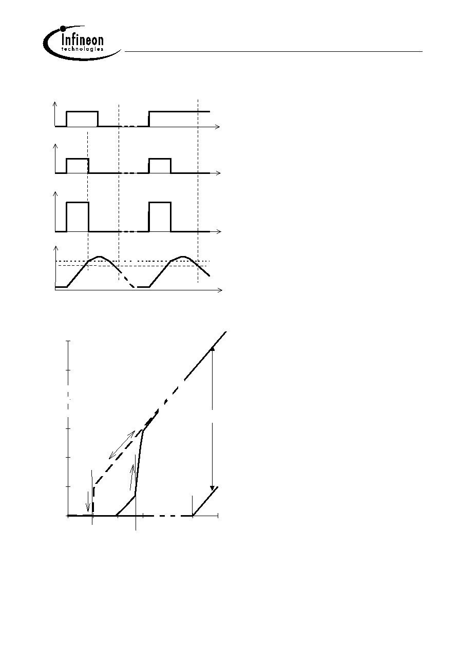
Maximum allowable load inductance for
a single switch off
L = f (IL );
Tj,start =
150∞C, Vbb =
12
V, RL =
0
L [µH]
IL [A]
Externally adjustable current limit
If the device is conducting, the sense current can be
used to reduce the short circuit current and allow
higher lead inductance (see diagram above). The
device will be turned off, if the threshold voltage of T2
is reached by I
S
*R
IS
. After a delay time defined by
R
V
*C
V
T1 will be reset. The device is turned on again,
the short circuit current is defined by I
L(SC)
and the
device is shut down after t
d(SC)
with latch function.
PROFET
IS
IN
IS
R
V
R
Power
GND
Signal
GND
Vbb
OUT
V
C
load
R
T1
T2
IN
Signal
Vbb
1
10
100
1000
10000
100000
1000000
1
10
100
1000
Data Sheet BTS555
Infineon Technologies AG
11
2003-Oct-01
Options Overview
Type BTS
6510
550P
650P
555
Overtemperature protection with hysteresis
X X X
Tj >150 ∞C, latch function
25
)
Tj >150 ∞C, with auto-restart on cooling
X
X
X
Short circuit to GND protection
with overtemperature shutdown
switches off when V
ON
>6 V typ.
(when first turned on after approx. 180
µ
s)
X
X
X
Overvoltage shutdown
- - -
Output negative voltage transient limit
to V
bb
- V
ON(CL)
X
X
X
to V
OUT
= -15 V typ
X
26)
X
26
)
X
26)
25
) Latch except when V
bb
-V
OUT
< V
ON(SC)
after shutdown. In most cases V
OUT
= 0 V after shutdown (V
OUT
0 V only if forced externally). So the device remains latched unless V
bb
< V
ON(SC)
(see page 5). No latch
between turn on and t
d(SC)
.
26
) Can be "switched off" by using a diode D
S
(see page 8) or leaving open the current sense output.

Data Sheet BTS555
Infineon Technologies AG
12
2003-Oct-01
Characteristics
Current sense versus load current:
I
IS
= f(I
L
)
I
IS
[mA]
I
L
[A]
Current sense ratio:
K
ILIS
= f(I
L
), T
J
= -40 ∞C
k
ilis
I
L
[A]
Current sense ratio:
K
ILIS
= f(I
L
), T
J
= 25 ∞C
k
ilis
I
L
[A]
Current sense ratio:
K
ILIS
= f(I
L
), T
J
= 150 ∞C
k
ilis
I
L
[A]
0
1
2
3
4
5
6
7
0
50
100
150
max
min
20000
25000
30000
35000
40000
45000
50000
55000
60000
65000
0
50
100
150
typ
max
min
20000
25000
30000
35000
40000
45000
50000
55000
60000
65000
0
50
100
150
typ
max
min
20000
25000
30000
35000
40000
45000
50000
55000
60000
65000
0
50
100
150
typ
max
min

Data Sheet BTS555
Infineon Technologies AG
13
2003-Oct-01
Typ. current limitation characteristic
I
L
= f (V
ON
, T
j
)
I
L
[A]
0
100
200
300
400
500
600
700
800
900
1000
0
10
15
20
T
j
= -40∞C
25∞C
85∞C
150∞C
V
ON(FB)
V
ON
>V
ON(SC)
only for t < t
d(SC)
(otherwise immediate shutdown)
V
ON
[V]
In case of V
ON
> V
ON(SC)
(typ. 6 V) the device will be
switched off by internal short circuit detection.
Typ. on-state resistance
R
ON
= f (V
bb
, T
j
)
; I
L
= 30
A; V
IN
= 0
R
ON
[mOhm]
0
1
2
3
4
5
6
0
5
10
15
20
static
dynamic
T
j
= 150∞C
85∞C
25∞C
-40∞C
40
V
bb
[V]
Typ. input current
I
IN
= f (V
bIN
), V
bIN =
V
bb
- V
IN
I
IN
[mA]
0
0.2
0.4
0.6
0.8
1.0
1.2
1.4
1.6
0
20
40
60
80
V
bIN
[V]
Data Sheet BTS555
Infineon Technologies AG
14
2003-Oct-01
Timing diagrams
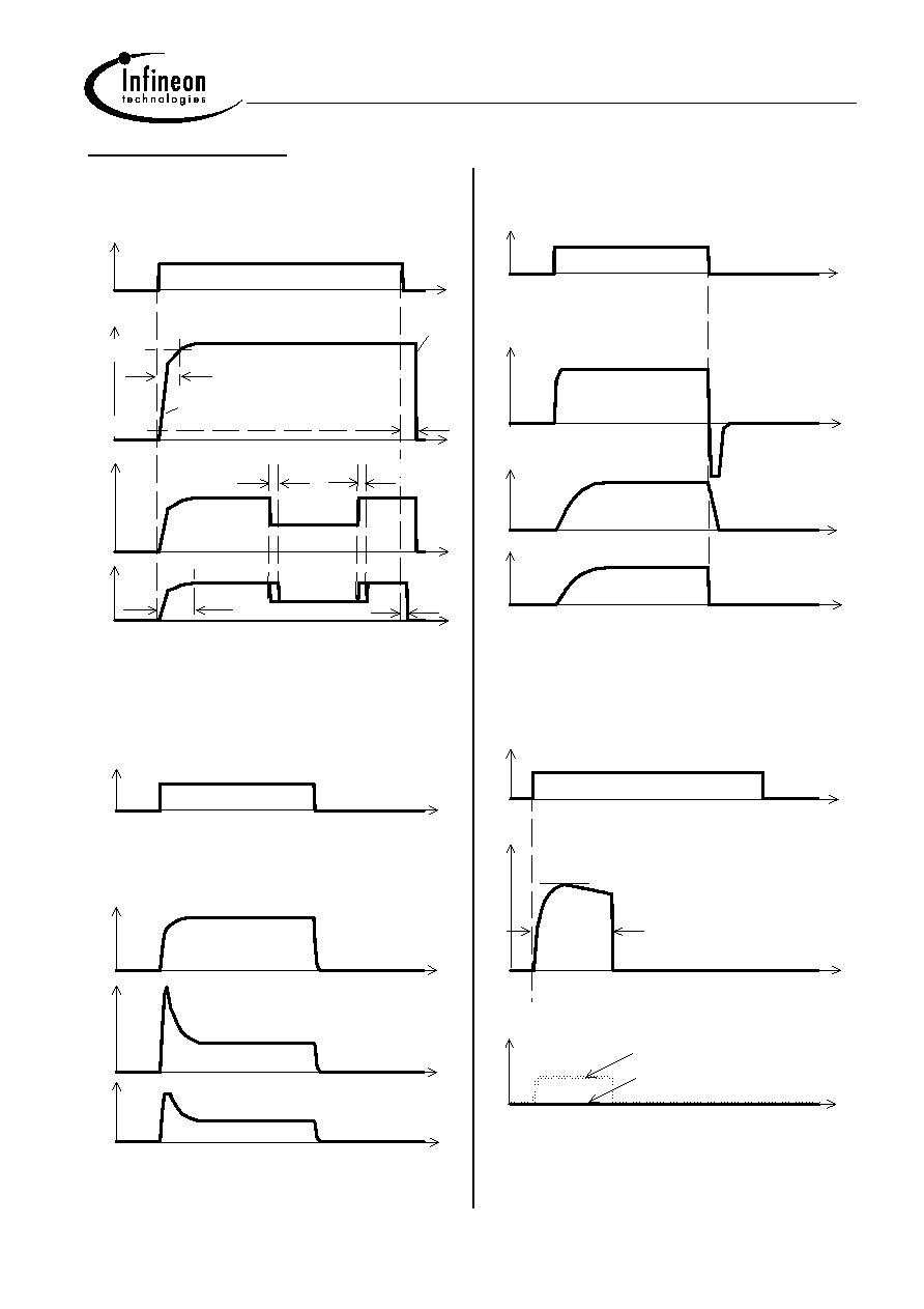
Figure 1a: Switching a resistive load,
change of load current in on-condition:
I
IN
t
V
OUT
I
L
I
IS
t
son(IS)
t
t
slc(IS)
Load 1
Load 2
soff(IS)
t
t
t
on
off
slc(IS)
90%
dV/dton
dV/dtoff
10%
The sense signal is not valid during a settling time
after turn-on/off and after change of load current.
Figure 2a: Switching motors and lamps:
I
IN
t
V
OUT
I
IL
I
IS
Sense current saturation can occur at very high
inrush currents (see I
IS,lim
on page 6).
Figure 2b: Switching an inductive load:
I
IN
t
V
OUT
I
L
I
IS
Figure 3a: Short circuit:
shut down by short circuit detection, reset by I
IN
=
0.
I
IN
I
L
I
L(SCp)
I
IS
t
t
d(SC)
V
OUT
=0
V
OUT
>>0
Shut down remains latched until next reset via input.
Data Sheet BTS555
Infineon Technologies AG
15
2003-Oct-01
Figure 4a: Overtemperature,
Reset if (I
IN
=low) and (T
j
<T
jt
)
IN
S
OUT
J
t
V
T
I
I
Figure 6a: Undervoltage restart of charge pump,
overvoltage clamp
0
2
4
6
0
V
OUT
V
bIN(ucp)
V
IN
= 0
I
IN
= 0
V
ON(CL)
V
bIN(u)
V
bIN(u)
dynamic, short
Undervoltage
not below
VON(CL)

Data Sheet BTS555
Infineon Technologies AG
16
2003-Oct-01
Package and Ordering Code
All dimensions in mm
TO-218AB/5 Option E3146
Ordering code
BTS555 E3146
Q67060-S6953A3
TO-218AB/5-1
Ordering
code
BTS555
Q67060-S6954
0.4
2)
1)
4.5
10.16
=
x
4
2.54
1.1
4.9
4
2.54
8.2
3.5
20.3
±0.2
+1
1
M
±0.3
+0.15
0.5
+0.3
12.5
2
-0.02
+0.1
16.3
+0.15
10
-0.25
±0.5
14
3)
+0.3
4.04
±0.2
10.8
14.8
±0.2
15
radii not dimensioned max. 0.2
Punch direction, burr max. 0.04
Dip tinning
Max. 15.5 by dip tinning
press burr max. 0.05
2)
3)
1)
±0.3
±0.5
11.5
Published by
Infineon Technologies AG,
St.-Martin-Strasse 53,
D-81669 M¸nchen
© Infineon Technologies AG 2001
All Rights Reserved.
Attention please!
The information herein is given to describe certain
components and shall not be considered as a guarantee of
characteristics.
Terms of delivery and rights to technical change reserved.
We hereby disclaim any and all warranties, including but not
limited to warranties of non-infringement, regarding circuits,
descriptions and charts stated herein.
Infineon Technologies is an approved CECC manufacturer.
Information
For further information on technology, delivery terms and
conditions and prices please contact your nearest Infineon
Technologies Office in Germany or our Infineon
Technologies Representatives worldwide (see address list).
Warnings
Due to technical requirements components may contain
dangerous substances. For information on the types in
question please contact your nearest Infineon Technologies
Office.
Infineon Technologies Components may only be used in life-
support devices or systems with the express written approval
of Infineon Technologies, if a failure of such components can
reasonably be expected to cause the failure of that life-
support device or system, or to affect the safety or
effectiveness of that device or system. Life support devices
or systems are intended to be implanted in the human body,
or to support and/or maintain and sustain and/or protect
human life. If they fail, it is reasonable to assume that the
health of the user or other persons may be endangered.