 | –≠–ª–µ–∫—Ç—Ä–æ–Ω–Ω—ã–π –∫–æ–º–ø–æ–Ω–µ–Ω—Ç: BUP311D | –°–∫–∞—á–∞—Ç—å:  PDF PDF  ZIP ZIP |
Semiconductor Group
1 May-06-1999
BUP 311D
IGBT With Antiparallel Diode
Preliminary data sheet
∑ Low forward voltage drop
∑ High switching speed
∑ Low tail current
∑ Latch-up free
∑ Including fast free-wheel diode
Former Development ID: BUP 3JKD
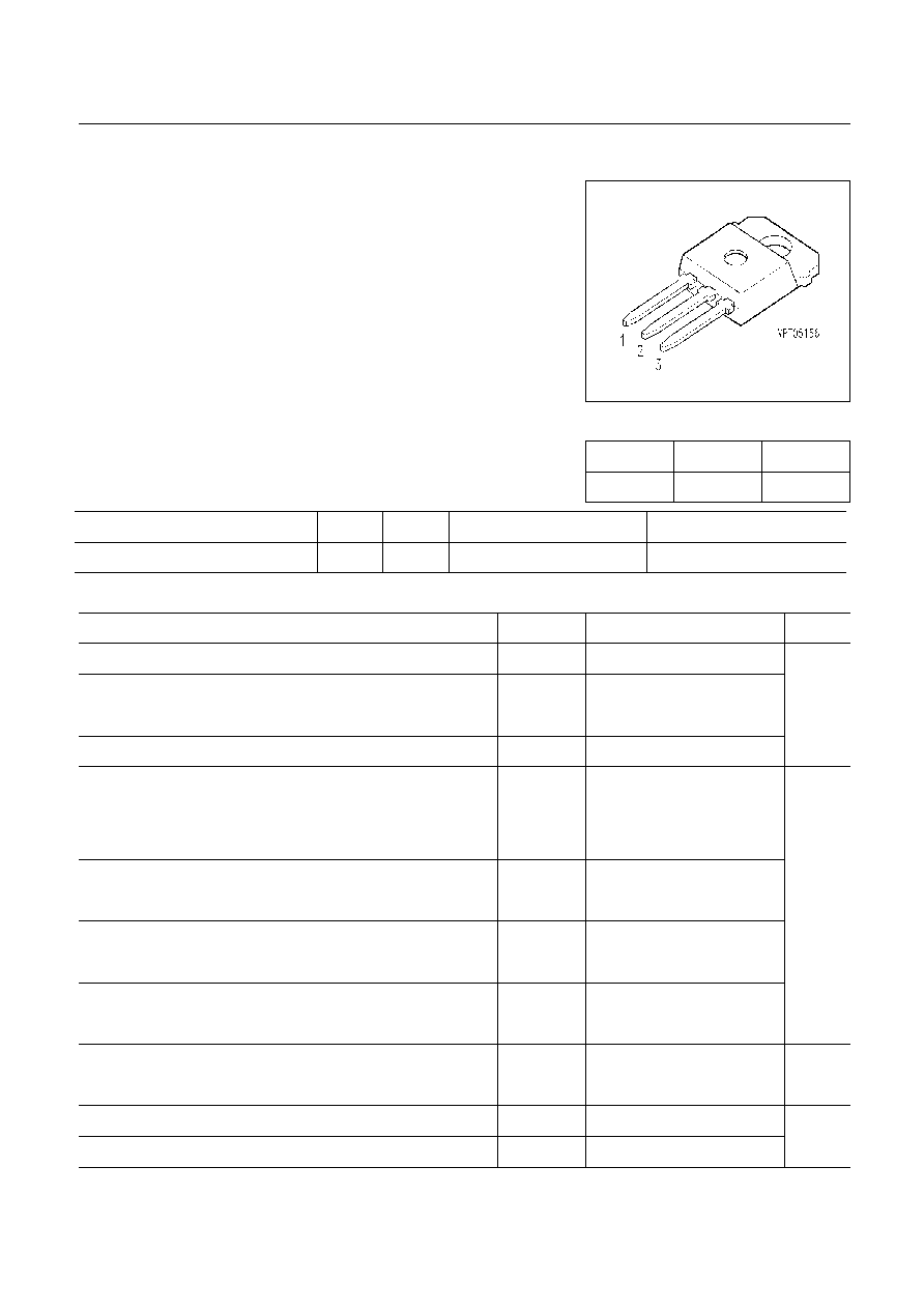
Pin 1
Pin 2
Pin 3
G
C
E
Type
V
CE
I
C
Package
Ordering Code
BUP 311D
1200V A
TO-218 AB
ON REQUEST
Maximum Ratings
Parameter
Symbol
Values
Unit
Collector-emitter voltage
V
CE
1200
V
Collector-gate voltage
R
GE
= 20 k
V
CGR
1200
Gate-emitter voltage
V
GE
± 20
DC collector current
T
C
= 25 ∞C
T
C
= 100 ∞C
I
C
12
20
A
Pulsed collector current,
t
p
= 1 ms
T
C
= 25 ∞C
I
Cpuls
40
Diode forward current
T
C
= 100 ∞C
I
F
tbd
Pulsed diode current,
t
p
= 1 ms
T
C
= 25 ∞C
I
Fpuls
tbd
Power dissipation
T
C
= 25 ∞C
P
tot
125
W
Chip or operating temperature
T
j
-55 ... + 150
∞C
Storage temperature
T
stg
-55 ... + 150
Infineon
C67078-A4102

Semiconductor Group
2
May-06-1999
BUP 311D
Maximum Ratings
Parameter
Symbol
Values
Unit
Chip or operating temperature
T
j
-55 ... + 150
∞C
Storage temperature
T
stg
-55 ... + 150
IEC climatic category, DIN IEC 68-1
-
55 / 150 / 56
-
Thermal Resistance
Thermal resistance, junction - case
R
thJC
1
K/W
Diode thermal resistance, chip case
R
thJC
D
2.5
Electrical Characteristics, at T
j
= 25 ∞C, unless otherwise specified
Parameter
Symbol
Values
Unit
min.
typ.
max.
Static Characteristics
Gate threshold voltage
V
GE
=
V
CE,
I
C
= 0.3 mA,
T
j
= 25 ∞C
V
GE(th)
4.5
5.5
6.5
V
Collector-emitter saturation voltage
V
GE
= 15 V,
I
C
= 8 A,
T
j
= 25 ∞C
V
GE
= 15 V,
I
C
= 8 A,
T
j
= 125 ∞C
V
GE
= 15 V,
I
C
= 16 A,
T
j
= 25 ∞C
V
GE
= 15 V,
I
C
= 16 A,
T
j
= 125 ∞C
V
CE(sat)
-
-
-
-
4.3
3.4
3.1
2.5
-
-
3.7
3
Zero gate voltage collector current
V
CE
= 1200 V,
V
GE
= 0 V,
T
j
= 25 ∞C
I
CES
-
-
0.4
mA
Gate-emitter leakage current
V
GE
= 25 V,
V
CE
= 0 V
I
GES
-
-
120
nA
Infineon

Semiconductor Group
3
May-06-1999
BUP 311D
AC Characteristics
Transconductance
V
CE
= 20 V,
I
C
= 8 A
g
fs
4
-
-
S
Input capacitance
V
CE
= 25 V,
V
GE
= 0 V,
f = 1 MHz
C
iss
-
600
tbd
pF
Output capacitance
V
CE
= 25 V,
V
GE
= 0 V,
f = 1 MHz
C
oss
-
60
tbd
Reverse transfer capacitance
V
CE
= 25 V,
V
GE
= 0 V,
f = 1 MHz
C
rss
-
38
tbd
Electrical Characteristics, at T
j
= 25 ∞C, unless otherwise specified
Parameter
Symbol
Values
Unit
min.
typ.
max.
Switching Characteristics, Inductive Load at T
j
= 125 ∞C
Turn-on delay time
V
CC
= 600 V,
V
GE
= 15 V,
I
C
= 8 A
R
Gon
= 150
t
d(on)
-
55
tbd
ns
Rise time
V
CC
= 600 V,
V
GE
= 15 V,
I
C
= 8 A
R
Gon
= 150
t
r
-
50
tbd
Turn-off delay time
V
CC
= 600 V,
V
GE
= -15 V,
I
C
= 8 A
R
Goff
= 150
t
d(off)
-
380
tbd
Fall time
V
CC
= 600 V,
V
GE
= -15 V,
I
C
= 8 A
R
Goff
= 150
t
f
-
80
tbd
Infineon

Semiconductor Group
4
May-06-1999
BUP 311D
Free-Wheel Diode
Diode forward voltage
I
F
= 8 A,
V
GE
= 0 V,
T
j
= 25 ∞C
I
F
= 8 A,
V
GE
= 0 V,
T
j
= 125 ∞C
V
F
-
-
tbd
tbd
-
tbd
V
Reverse recovery time
I
F
= 8 A,
V
R
= -600 V,
V
GE
= 0 V
di
F
/
dt = -400 A/µs, T
j
= 25 ∞C
t
rr
-
tbd tbd
ns
Reverse recovery charge
I
F
= 15 A,
V
R
= -600 V,
V
GE
= 0 V
di
F
/
dt = -400 A/µs
T
j
= 25 ∞C
T
j
= 125 ∞C
Q
rr
-
-
tbd
tbd
tbd
tbd
µC
Infineon
Semiconductor Group
5
May-06-1999
BUP 311D
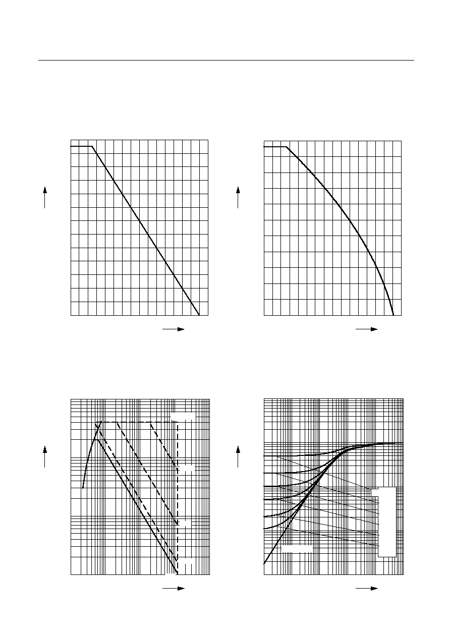
Power dissipation
P
tot
=
(T
C
)
parameter: T
j
150 ∞C
0
20
40
60
80
100
120
∞C
160
T
C
0
10
20
30
40
50
60
70
80
90
100
110
W
130
P
tot
Collector current
I
C
=
(T
C
)
parameter: V
GE
15 V , T
j
150 ∞C
0
20
40
60
80
100
120
∞C
160
T
C
0
2
4
6
8
10
12
14
16
18
A
22
I
C
Safe operating area
I
C
=
(V
CE
)
parameter: D = 0, T
C
= 25∞C , T
j
150 ∞C
-1
10
0
10
1
10
2
10
A
I
C
10
0
10
1
10
2
10
3
V
V
CE
DC
10 ms
1 ms
100 µs
t
p
= 15.0µs
Transient thermal impedance IGBT
Z
th JC
=
(t
p
)
parameter: D = t
p
/ T
-3
10
-2
10
-1
10
0
10
1
10
K/W
Z
thJC
10
-5
10
-4
10
-3
10
-2
10
-1
10
0
s
t
p
single pulse
0.01
0.02
0.05
0.10
0.20
D = 0.50
Infineon
Semiconductor Group
6
May-06-1999
BUP 311D
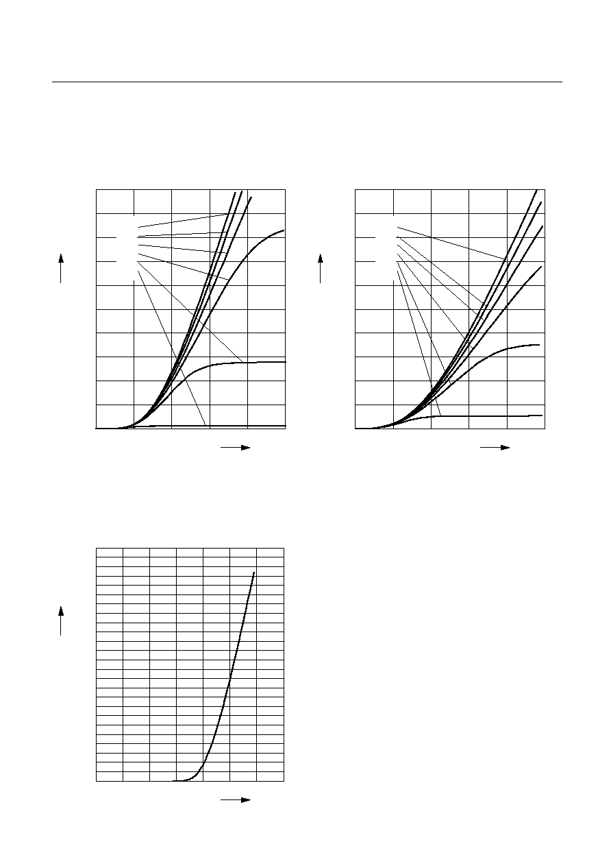
Typ. output characteristics
I
C
=
f (V
CE
)
parameter:
t
p
= 80 µs,
T
j
= 25 ∞C
0
1
2
3
V
5
V
CE
0
2
4
6
8
10
12
14
16
A
20
I
C
17V
15V
13V
11V
9V
7V
Typ. output characteristics
I
C
= f (V
CE
)
parameter:
t
p
= 80 µs,
T
j
= 125 ∞C
0
1
2
3
V
5
V
CE
0
2
4
6
8
10
12
14
16
A
20
I
C
17V
15V
13V
11V
9V
7V
Typ. transfer characteristics
I
C
=
f (V
GE
)
parameter:
t
p
= 80 µs,
V
CE
= 20 V
0
2
4
6
8
10
V
14
V
GE
0
2
4
6
8
10
12
14
16
18
20
22
A
25
I
C
Infineon

Semiconductor Group
7
May-06-1999
BUP 311D
Typ. switching time
t = f (R
G
)
, inductive load ,
T
j
= 125∞C
par.:
V
CE
=600V,
V
GE
= ±15V,
I
C
=8 A
0
50
100 150 200 250 300 350 400
500
R
G
1
10
2
10
3
10
ns
t
tdon
tr
tdoff
tf
Typ. switching time
t = f (I
C
)
, inductive load , T
j
= 125∞C
par.:
V
CE
=600V,
V
GE
= ±15V,
R
G
=153
0
4
8
12
16
20
24
A
30
I
C
1
10
2
10
3
10
ns
t
tdon
tr
tdoff
tf
Typ. switching losses
E = f (I
C
)
,
inductive load ,
T
j
= 125∞C
par.:
V
CE
=600V,
V
GE
= ±15V,
R
G
=153
0
4
8
12
16
20
24
A
30
I
C
0
1
2
3
4
5
6
7
8
mWs
10
E
Eon
Eoff
Typ. switching losses
E = f (R
G
)
, inductive load , T
j
= 125∞C
par.:
V
CE
=600V,
V
GE
= ±15V,
I
C
=8 A
0
50
100 150 200 250 300 350 400
500
R
G
0
1
2
3
4
5
6
7
8
mWs
10
E
Eon
Eon
Infineon

Semiconductor Group
8
May-06-1999
BUP 311D
Typ. gate charge
V
GE
=
(Q
Gate
)
parameter: I
C puls
= 15 A
0
-4
-8
-12
-16
-20
-28
Q
Gate
0
2
4
6
8
10
12
14
16
V
20
V
GE
Typ. capacitances
C = f (V
CE
)
0
5
10
15
20
25
30
V
40
V
CE
1
10
2
10
3
10
4
10
pF
C
C
iss
C
oss
C
rss
Short circuit safe operating area
I
Csc
= f (V
CE
) , T
j
= 150∞C
parameter:
V
GE
= ± 15 V,
t
sc
10 µs, L < 25 nH
0
200
400
600
800
1000 1200
V
1600
V
CE
0
2
4
6
10
I
Csc
/I
C(90∞C)
Reverse biased safe operating area
I
Cpuls
= f (V
CE
) , T
j
= 150∞C
parameter:
V
GE
= 15 V
0
200
400
600
800
1000 1200
V
1600
V
CE
0.0
0.5
1.0
1.5
2.5
I
Cpuls
/I
C
Infineon

Semiconductor Group
9
May-06-1999
BUP 311D
Typ. forward characteristics
I
F
=
f (V
F
)
parameter:
T
j
0.0
0.5
1.0
1.5
2.0
V
3.0
V
F
0
2
4
6
8
10
12
14
16
18
20
22
24
26
A
30
I
F
T
j
=25∞C
=125∞C
j
T
Transient thermal impedance Diode
Z
th JC
=
(t
p
)
parameter: D = t
p
/ T
-2
10
-1
10
0
10
1
10
K/W
Z
thJC
10
-5
10
-4
10
-3
10
-2
10
-1
10
0
s
t
p
single pulse
0.01
0.02
0.05
0.10
0.20
D = 0.50
Infineon