Mar-10-2004
1
SMBD7000/MMBD7000...
Silicon Switching Diode Array
·
For high-speed switching applications
SMBD7000/MMBD7000
3
1
D 2
2
D 1
Type
Package
Configuration
Marking
SMBD7000/MMBD7000
SOT23
series
s5C
Maximum Ratings at T
A
= 25°C, unless otherwise specified
Parameter
Symbol
Value
Unit
Diode reverse voltage
V
R
100
V
Peak reverse voltage
V
RM
100
Forward current
I
F
200
mA
Non-repetitive peak surge forward current
t = 1 µs
t = 1 s
I
FSM
4.5
0.5
A
Total power dissipation
T
S
28°C
P
tot
330
mW
Junction temperature
T
j
150
°C
Storage temperature
T
stg
-65 ... 150
Thermal Resistance
Parameter
Symbol
Value
Unit
Junction - soldering point
1)
SMBD7000/MMBD7000
R
thJS
360
K/W
1
For calculation of R
thJA
please refer to Application Note Thermal Resistance
Mar-10-2004
2
SMBD7000/MMBD7000...
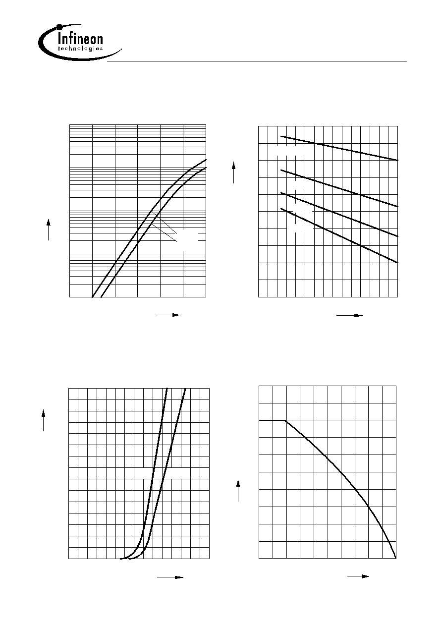
Electrical Characteristics at T
A
= 25°C, unless otherwise specified
Parameter
Symbol
Values
Unit
min.
typ.
max.
DC Characteristics
Breakdown voltage
I
(BR)
= 100 µA
V
(BR)
100
-
-
V
Reverse current
V
R
= 50 V
V
R
= 100 V
V
R
= 50 V, T
A
= 150 °C
I
R
-
-
-
-
-
-
0.3
0.5
100
µA
Forward voltage
I
F
= 1 mA
I
F
= 10 mA
I
F
= 50 mA
I
F
= 100 mA
I
F
= 150 mA
V
F
550
670
-
750
-
-
-
-
-
-
700
820
1000
1100
1250
mV
AC Characteristics
Diode capacitance
V
R
= 0 V, f = 1 MHz
C
T
-
-
2
pF
Reverse recovery time
I
F
= 10 mA, I
R
= 10 mA, measured at I
R
= 1mA,
R
L
= 100
t
rr
-
-
4
ns
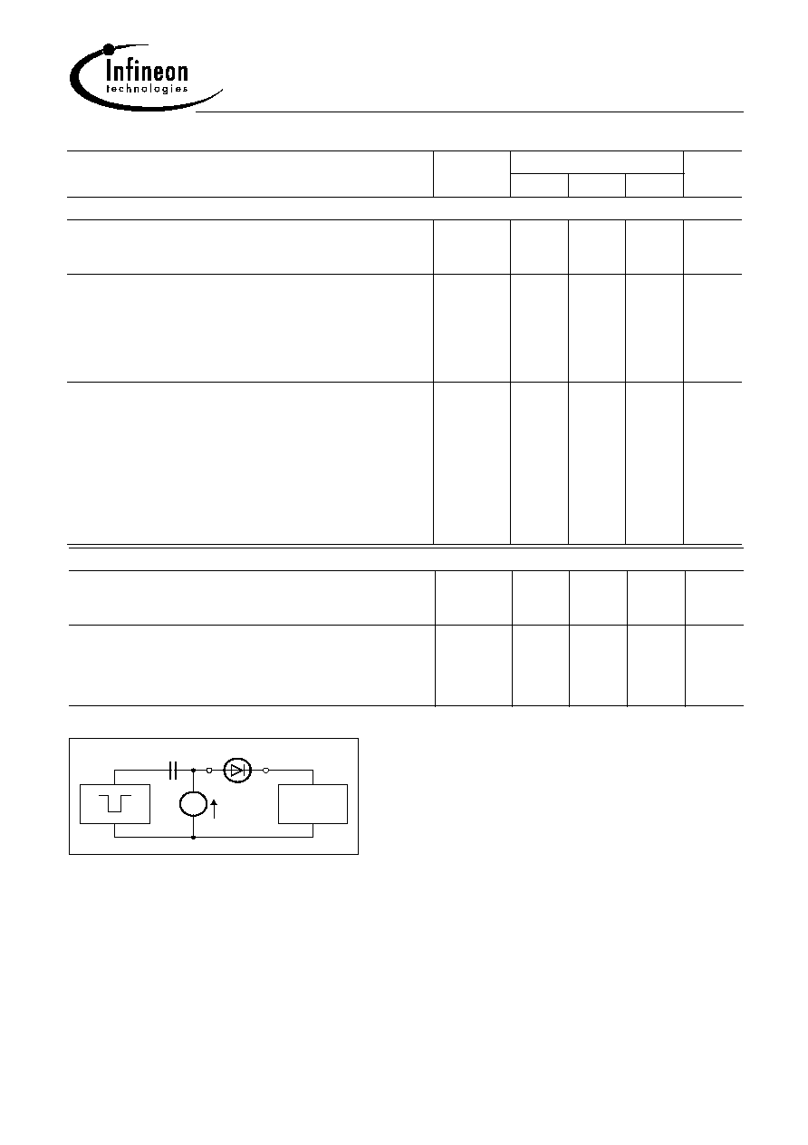
Test circuit for reverse recovery time
EHN00019
F
D.U.T.
Oscillograph
Pulse generator: t
p
= 100ns, D = 0.05, t
r
= 0.6ns,
R
i
= 50
Oscillograph: R = 50
, t
r
= 0.35ns, C
1pF
Mar-10-2004
4
SMBD7000/MMBD7000...
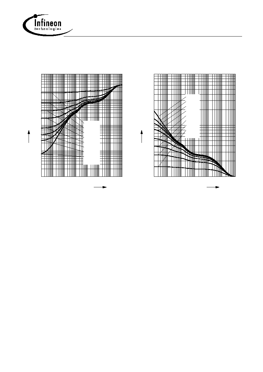
Permissible Puls Load R
thJS
=
(t
p
)
10
-7
10
-6
10
-5
10
-4
10
-3
10
-2
10
0
s
T
P
-1
10
0
10
1
10
2
10
3
10
R
thJS
D = 0,5
0,2
0,1
0,05
0,02
0,01
0,005
0
Permissible Pulse Load
I
Fmax
/ I
FDC
=
(t
p
)
10
-6
10
-5
10
-4
10
-3
10
-2
10
0
s
T
P
0
10
1
10
2
10
-
I
Fmax
/
I
FDC
D = 0
0.005
0.01
0.02
0.05
0.1
0.2
0.5