1
2001-07-25
SPI11N60S5
SPP11N60S5, SPB11N60S5
Preliminary data
Cool MOSTM
=
=
=
=
Power Transistor
∑
=
New revolutionary high voltage technology
∑
Ultra low gate charge
∑
=
Periodic avalanche rated
∑
Extreme dv/dt rated
∑
=
Optimized capacitances
∑
=
Improved noise immunity
∑
=
Former development designation:
SPPx2N60S5/SPBx2N60S5
C
Power Semiconductors
O
O L
MOS
Product Summary
V
DS
@ T
jmax
650
V
R
DS(on)
0.38
I
D
11
A
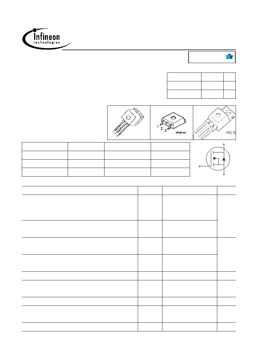
P-TO262
P-TO263-3-2
P-TO220-3-1
G,1
D,2
S,3
Marking
11N60S5
11N60S5
11N60S5
Type
Package
Ordering Code
SPP11N60S5
P-TO220-3-1
Q67040-S4198
SPB11N60S5
P-TO263-3-2
Q67040-S4199
SPI11N60S5
P-TO262
Q67040-S4338
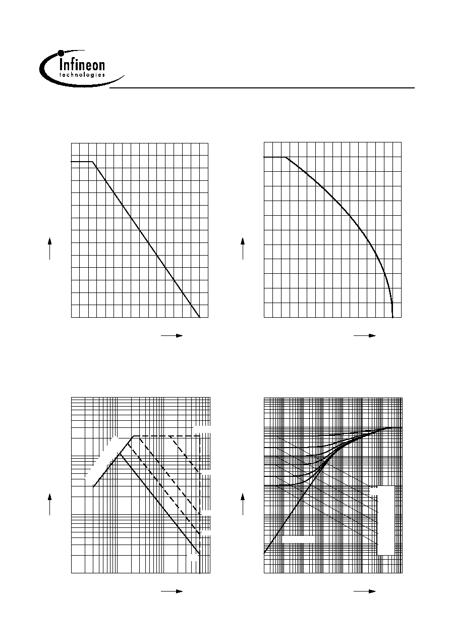
Maximum Ratings,at T
j
= 25 ∞C, unless otherwise specified
Parameter
Symbol
Value
Unit
Continuous drain current
T
C
=25∞C
T
C
=100∞C
I
D
11
7
A
Pulsed drain current
1)
T
C
=25∞C
I
D puls
22
Avalanche energy, single pulse
I
D
= 5.5 A, V
DD
= 50 V
E
AS
340
mJ
Avalanche energy (repetitive, limited by T
jmax
)
I
D
= 11 A, V
DD
= 50 V
E
AR
0.6
Avalanche current (repetitive, limited by T
jmax
)
I
AR
11
A
Reverse diode dv/dt
I
S
=11A, V
DS
<V
DSS
, di/dt=100A/µs, T
jmax
=150∞C
dv/dt
6
kV/µs
Gate source voltage
V
GS
±
20
V
Power dissipation
T
C
=25∞C
P
tot
125
W
Operating and storage temperature
T
j ,
T
stg
-55... +150
∞C

2
2001-07-25
SPI11N60S5
SPP11N60S5, SPB11N60S5
Preliminary data
Electrical Characteristics, at T
j
= 25 ∞C, unless otherwise specified
Parameter
Symbol
Values
Unit
min.
typ.
max.
Thermal Characteristics
Thermal resistance, junction - case
R
thJC
-
-
1
K/W
Thermal resistance, junction - ambient
(Leaded and through-hole packages)
R
thJA
-
-
62
SMD version, device on PCB:
@ min. footprint
@ 6 cm
2
cooling area
2)
R
thJA
-
-
-
35
62
-
Static Characteristics, at T
j
= 25 ∞C, unless otherwise specified
Drain-source breakdown voltage
V
GS
= 0 V, I
D
= 0.25 mA
V
(BR)DSS
600
-
-
V
Gate threshold voltage, V
GS
= V
DS
I
D
= 0.5 mA, T
j
= 25 ∞C
V
GS(th)
3.5
4.5
5.5
Zero gate voltage drain current, V
DS
=V
DSS
V
GS
= 0 V, T
j
= 25 ∞C
V
GS
= 0 V, T
j
= 150 ∞C
I
DSS
-
-
-
-
25
250
µA
Gate-source leakage current
V
GS
= 20 V, V
DS
= 0 V
I
GSS
-
-
100
nA
Drain-source on-state resistance
V
GS
= 10 V, I
D
= 7 A
R
DS(on)
-
0.34
0.38
1current limited by Tjmax
2 Device on 40mm*40mm*1.5mm epoxy PCB FR4 with 6 cm
≤
(one layer, 70µm thick) copper area for drain
connection. PCB is vertical without blown air.
3
2001-07-25
SPI11N60S5
SPP11N60S5, SPB11N60S5
Preliminary data
Electrical Characteristics, at T
j
= 25 ∞C, unless otherwise specified
Parameter
Symbol
Conditions
Values
Unit
min.
typ.
max.
Dynamic Characteristics
Transconductance
g
fs
V
DS
2*I
D
*R
DS(on)max
,
I
D
=7A
-
6
-
S
Input capacitance
C
iss
V
GS
=0V, V
DS
=25V,
f=1MHz
-
1460
-
pF
Output capacitance
C
oss
-
610
-
Reverse transfer capacitance
C
rss
-
21
-
Turn-on delay time
t
d(on)
V
DD
=350V, V
GS
=10V,
I
D
=11A, R
G
=6.8
-
130
-
ns
Rise time
t
r
-
35
-
Turn-off delay time
t
d(off)
-
150
225
Fall time
t
f
-
20
30
Gate Charge Characteristics
Gate to source charge
Q
gs
V
DD
=350V, I
D
=11A
-
10.5
-
nC
Gate to drain charge
Q
gd
-
24
-
Total gate charge
Q
g
V
DD
=350V, I
D
=11A,
V
GS
=0 to 10V
-
41.5
54
Reverse Diode
Inverse diode continuous
forward current
I
S
T
C
=25∞C
-
-
11
A
Inverse diode direct
current,pulsed
I
SM
-
-
22
Inverse diode forward voltage V
SD
V
GS
=0V, I
F
=11A
-
1
1.2
V
Reverse recovery time
t
rr
V
R
=350V, I
F=
l
S
,
di
F
/dt=100A/µs
-
650
1105 ns
Reverse recovery charge
Q
rr
-
7.9
-
µC
5
2001-07-25
SPI11N60S5
SPP11N60S5, SPB11N60S5
Preliminary data
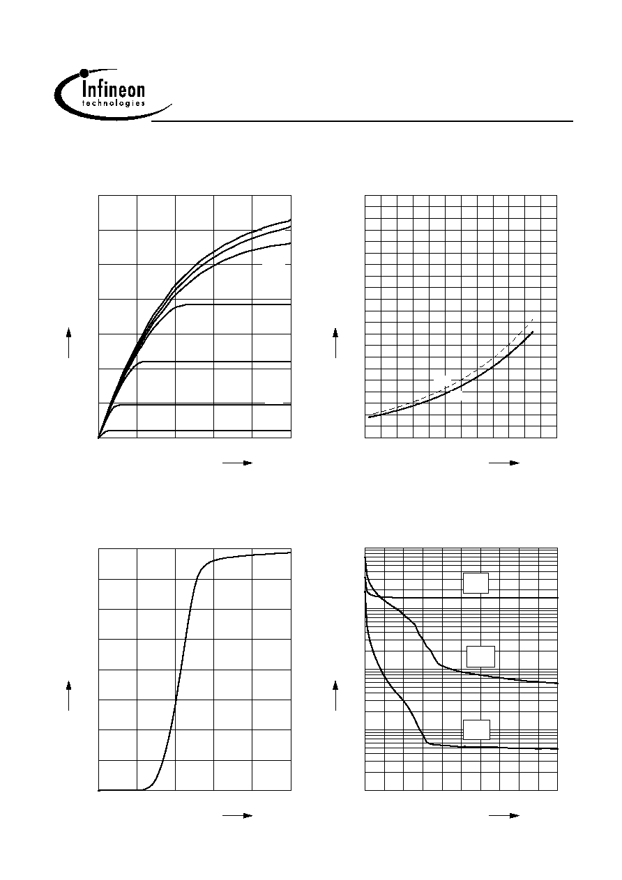
Typ. output characteristic
I
D
= f (V
DS
)
Parameter: V
GS
, T
j
= 25 ∞C
0
5
10
15
V
25
V
DS
0
5
10
15
20
25
A
35
I
D
6V
7V
8V
9V
10V
12V
20V
Drain-source on-resistance
R
DS(on)
= f (T
j
)
parameter : I
D
= 7 A, V
GS
= 10 V
-60
-20
20
60
100
∞C
180
T
j
0
0.2
0.4
0.6
0.8
1
1.2
1.4
1.6
1.8
2.1
SPP11N60S5
R
DS(on)
typ
98%
Typ. capacitances
C = f (V
DS
)
parameter: V
GS
=0 V, f=1 MHz
0
10
20
30
40
50
60
70
80
V
100
V
DS
0
10
1
10
2
10
3
10
4
10
pF
C
C
iss
C
oss
C
rss
Typ. transfer characteristics
I
D
= f ( V
GS
)
V
DS
2 x I
D
x R
DS(on)max
0
4
8
12
V
GS
20
V
0
4
8
12
16
20
24
A
32
I
D