 | –≠–ª–µ–∫—Ç—Ä–æ–Ω–Ω—ã–π –∫–æ–º–ø–æ–Ω–µ–Ω—Ç: 8XC196MD | –°–∫–∞—á–∞—Ç—å:  PDF PDF  ZIP ZIP |

Other brands and names are the property of their respective owners
Information in this document is provided in connection with Intel products Intel assumes no liability whatsoever including infringement of any patent or
copyright for sale and use of Intel products except as provided in Intel's Terms and Conditions of Sale for such products Intel retains the right to make
changes to these specifications at any time without notice Microcomputer Products may have minor variations to this specification known as errata
April 1994
COPYRIGHT
INTEL CORPORATION 1995
Order Number 272323-002
8XC196MD
INDUSTRIAL MOTOR CONTROL
MICROCONTROLLER
87C196MD 16 Kbytes of On-Chip OTPROM
87C196MD ROM 16 Kbytes of On-Chip Factory-Programmed OTPROM
80C196MD ROMless
Y
High-Performance CHMOS 16-Bit CPU
Y
16 Kbytes of On-Chip OTPROM
Factory-Programmed OTPROM
Y
488 bytes of On-Chip Register RAM
Y
Register to Register Architecture
Y
Up to 64 I O Lines
Y
Peripheral Transaction Server (PTS)
with 17 Prioritized Sources
Y
Event Processor Array (EPA)
6 High Speed Capture Compare
Modules
6 High Speed Compare Modules
Y
Extended Temperature Standard
Y
Programmable Frequency Generator
Y
Two 16-Bit Timers with Quadrature
Counting Input
Y
3-Phase Complementary Waveform
Generator
Y
14 Channel 8 10-Bit A D with Sample
Hold with Zero Offset Adjustment H W
Y
18 Prioritized Interrupt Sources
Y
Flexible 8- 16-Bit External Bus
Y
1 75 ms 16 x 16 Multiply
Y
3 ms 32 16 Divide
Y
Idle and Power Down Modes
The 8XC196MD is a 16-bit microcontroller designed primarily to control 3 phase AC induction and DC brush-
less motors The 8XC196MD is based on Intel's MCS
96 16-bit microcontroller architecture and is manufac-
tured with Intel's CHMOS process
The 8XC196MD has a three phase waveform generator specifically designed for use in ``Inverter'' motor
control applications This peripheral allows for pulse width modulation three phase sine wave generation with
minimal CPU intervention It generates 3 complementary non-overlapping PWM pulses with resolutions of
0 125 ms (edge trigger) or 0 250 ms (centered)
The 8XC196MD has 16 Kbytes on-chip OTPROM ROM and 488 bytes of on-chip RAM It is available in two
packages PLCC (84-L) and EIAJ QFP (80-L)
Operational characteristics are guaranteed over the temperature range of b40 C to a85 C
The 87C196MD contains 16 Kbytes on-chip OTPROM The 83C196MD contains 16 Kbytes on-chip ROM All
references to the 80C196MD also refers to the 83C196MD and 87C196MD unless noted
OTPROM (One Time Programmable Read Only Memory) is the same as EPROM but it comes in an unwindowed package
and cannot be erased It is user programmable
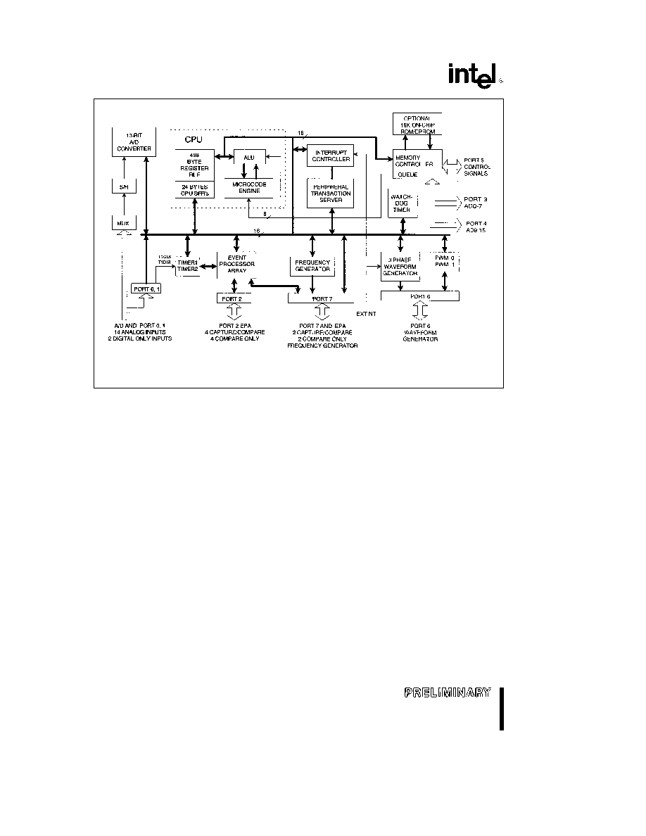
8XC196MD
272323 ≠ 1
NOTE
Connections between the standard I O ports and the bus are not shown
Figure 1 87C196MD Block Diagram
2
8XC196MD
PROCESS INFORMATION
This device is manufactured on PX29 5 a CHMOS
III-E process Additional process and reliability infor-
mation is available in Intel's
Components Quality
and Reliability Handbook
Order Number 210997
272323 ≠ 2
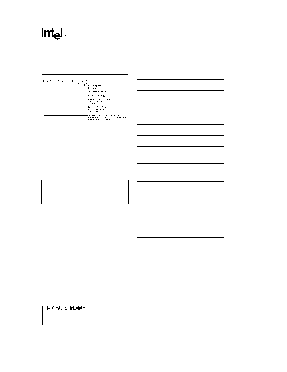
EXAMPLE
N87C196MD is 84-Lead PLCC OTPROM
16 MHz
For complete package dimensional data refer to the
Intel Packaging Handbook (Order Number 240800)
NOTE
EPROMs are available as One Time Programmable
(OTPROM) only
Figure 2 The 8XC196MD Family Nomenclature
Table 1 Thermal Characteristics
Package
i
ja
i
jc
Type
PLCC
35 C W
13 C W
QFP
56 C W
12 C W
All thermal impedance data is approximate for static air
conditions at 1W of power dissipation Values will change
depending on operation conditions and application See
the Intel
Packaging Handbook (order number 240800) for a
description of Intel's thermal impedance test methodology
Table 2 8XC196MD Memory Map
Description
Address
External Memory or I O
0FFFFH
06000H
Internal ROM EPROM or External
5FFFH
Memory (Determined by EA)
2080H
Reserved Must contain FFH
207FH
(Note 5)
205EH
PTS Vectors
205DH
2040H
Upper Interrupt Vectors
203FH
2030H
ROM EPROM Security Key
202FH
2020H
Reserved Must contain FFH
201FH
(Note 5)
201CH
Reserved Must Contain 20H
201BH
(Note 5)
CCB1
201AH
Reserved Must Contain 20H
2019H
(Note 5)
CCB0
2018H
Reserved Must contain FFH
2017H
(Note 5)
2014H
Lower Interrupt Vectors
2013H
2000H
SFR's
1FFFH
1F00H
External Memory
1EFFH
0200H
488 Bytes Register RAM (Note 1)
01FFH
0018H
CPU SFR's (Notes 1 3)
0017H
0000H
NOTES
1 Code executed in locations 0000H to 01FFH will be
forced external
2 Reserved memory locations must contain 0FFH unless
noted
3 Reserved SFR bit locations must contain 0
4 Refer to 8XC196MC for SFR descriptions
5 WARNING Reserved memory locations must not be
written or read The contents and or function of these lo-
cations may change with future revisions of the device
Therefore a program that relies on one or more of these
locations may not function properly
3

8XC196MD
8XC196MC AND 8XC196MD
DIFFERENCES
INT
MASK1 INT
PEND1 Registers
There
are
some
differences
between
the
8XC196MC
and
8XC196MD
INT
MASK1
INT
PEND1 registers
The 8XC196MD interrupt
mask and pending registers are shown below No-
tice that the CAPCOM5 COMP4 and CAPCOM4
bits are reserved bits on the 8XC196MC The PI bit
of the INT
PEND1 register will be set when a
Waveform Generator or Compare Module 5 event
occurs and the corresponding bit in the PI
MASK
register is set The PI interrupt vector can be taken
when the PI bit in the INT
MASK1 register is set
The 8XC196MC User's Manual should be refer-
enced for details about the interrupts
INT
MASK1 (0031H)
and INT
PEND1 (0012H)
7
6
5
4
3
2
1
0
RSV EXTINT
PI
CAPCOM5 COMP4 CAPCOM4 COMP3 CAPCOM3
RSV
e
RESERVED BIT MUST WRITE AS 0
e
THIS BIT RESERVED ON 8XC196MC
Figure 3 Interrupt Mask and Status Registers
PTSSRV and PTSSEL Register
Similarly there are differences between 8XC196MC
and 8XC196MD PTS registers The 8XC196MD PTS
registers are shown below Notice the CAPCOM5
COMP4 and CAPCOM4 bits are reserved bits on
the 8XC196MC The PI bit in the PTSSRV will be set
when a Waveform Generator or Compare Module 5
end of PTS interrupt occurs and the corresponding
bit in the PI
MASK register is set The PI PTS vec-
tor can be used when the PI bit in the PTSSEL regis-
ter is set The 8XC196MC User's Manual should be
referenced for details about the PTS
PTSSEL (0004H) and PTSSRV (0006H)
15
14
13
12
11
10
9
8
RSV
EXTINT
PI
CAPCOM5
COMP4
CAPCOM4
COMP3 CAPCOM3
7
6
5
4
3
2
1
0
COMP2 CAPCOM2 COMP1 CAPCOM1 COMP0 CAPCOM0 AD
DONE TOVF
RSV
e
RESERVED BIT MUST WRITE AS 0
e
THIS BIT RESERVED ON 8XC196MC
Figure 4 PTS Select and Service Registers
PI
MASK and PI
PEND Registers
The PI
MASK PI
PEND registers contain the bits
for the Compare Module 5 (COMP5) Waveform Gen-
erator (WG) Timer 1 Overflow (TFI) and Timer 2
Overflow (TF2) mask status flag The diagram be-
low shows the registers Notice that the COMP5 bit
is a reserved bit on the 8XC196MC The 8XC196MC
User's Manual should be referenced for details
about the Waveform Generator Compare Modules
and Timers
PI
MASK (1FBEH) and
PI
PEND (1FBCH Read Only)
7
6
5
4
3
2
1
0
RSV
COMP5
RSV
WG
RSV
TF2
RSV
TF1
RSV
e
RESERVED BIT MUST WRITE AS 0
READ AS 1
e
THIS BIT RESERVED ON 8XC196MC
Figure 5 Peripheral Interrupt Mask
and Status Registers
The PI bit in the INT
PEND1 register is set if a
Waveform Generator event or Compare Module 5
event occurs and the corresponding PI
MASK bit is
set For either of these events to cause an interrupt
the PI bit in the INT
MASK1 register and the corre-
sponding event bit in the PI
MASK register must be
set
Similarly the TOVF bit in the INT
PEND register is
set if Timer 1 or Timer 2 overflow and the corre-
sponding bit in the PI
MASK register is set For ei-
ther of these two events to cause an interrupt the
TOVF bit in the INT
MASK register and the corre-
sponding event bit in the PI
MASK must be set
Upon a PI and or a TOVF interrupt it may be neces-
sary to check if the Compare Module 5 the Wave-
form Generator Timer 1 or Timer 2 event caused
the interrupt The PI
PEND will give this informa-
tion However it should be noted that reading the
PI
PEND register will clear the register So the indi-
vidual bits in the PI
PEND register must be read by
loading PI
PEND into another ``shadow'' register
then checking the ``shadow'' register to see what
event occurred
4
8XC196MD
Table 3 Interrupt Sources Vectors and Priorities
Interrupt Service
PTS Service
Interrupt Source
Symbol
Name
Vector
Priority
Name
Vector
Priority
Capture Compare5
CAPCOMP5
INT12
2038H
12
PTS12
2058H
27
Compare4
COMP4
INT11
2036H
11
PTS11
2056H
26
Capture Compare4
CAPCOMP4
INT10
2034H
10
PTS10
2054H
25
Interrupt and PTS Vectors
The 8XC196MD has three new interrupt and PTS
vectors which are Capture Compare5 Compare 4
and Capture Compare4 Table 3 shows these inter-
rupt vectors and priorities These are shown as re-
served vectors in the 8XC196MC User's Manual
Frequency Generator
The Frequency Generator (FG) Peripheral which
was not available on the 8XC196MC device is avail-
able on the 8XC196MD device The FG outputs a
programmable-frequency 50% duty cycle waveform
on the FREQOUT pin (P7 7) There are two 8-bit reg-
isters which control the FG peripheral
Frequency Generator Control Register
(FG
CON) at 1FB8h
Frequency Generator Period Count Register
(FG
COUNT) at 1FBAh
The FG
CON can be read or written This register
is loaded with a value which determines the number
of counts necessary for toggling the output The fol-
lowing equation should be used to calculate the
FG
CON value
FG
CON value
e
F
XTAL
16
(FG Frequency)
b
1
where FG Frequency is from 4 kHz to 1 MHz
The FG
COUNT is loaded with the FG
CON reg-
ister value The FG
COUNT register is decrement-
ed every eighth state time When it reaches 00h the
FG
COUNT register will send a signal to toggle the
output pin and reload the FG
COUNT register with
the
value
in
the
FG
CON
register
The
FG
COUNT can only be read not written
The FREQOUT pin (P7 7) must be configured for a
special function to use it for the Frequency Genera-
tor feature
Port 7
Port 7 is an additional bidirectional port that was not
available on the 8XC196MC device Port 7 can be
used as I O or some of the pins have special func-
tions The pins are listed below followed by their
special functions
Table 4 Port 7 Special Function Pins
Pin
Special Function
P7 0
CAPCOMP4
P7 1
CAPCOMP5
P7 2
CAPCOMP4
P7 3
CAPCOMP5
P7 4
P7 5
P7 6
P7 7
FREQOUT
The special functions of the pins are selected in the
Port 7 SFRs The Port 2 I O Port section of the
8XC196MC User's Manual can be referenced when
setting up the Port 7 SFRs Port 7 SFRs are located
in the following locations
Table 5 Port 7 Special Function Registers
SFR
Address
P7
MODE
1FD1h
P7
DIR
1FD3h
P7
REG
1FD5h
P7
PIN
1FD7h
5

8XC196MD
Port 1
There are three additional Port 1 input pins (P1 5 ≠
P1 7) that were not available on the 8XC196MC
These pins are listed below followed by their func-
tion
Table 6 New 8XC196MD Port 1 Pins
Pin
Description
P1 5
Digital or Analog Input
P1 6
Digital Input
P1 7
Digital Input
NOTE
P1 5 was a V
SS
pin on the 8XC196MC device If
P1 5 and P1 6 are not being used these pins can
remain connected to V
SS
6
8XC196MD
272323 ≠ 3
NOTE
NC means No Connect Do not connect these pins
Figure 6 84-Lead PLCC Package
7

8XC196MD
272323 ≠ 4
Figure 7 80-Lead Shrink EIAJQFP (Quad Flat Pack)
8

8XC196MD
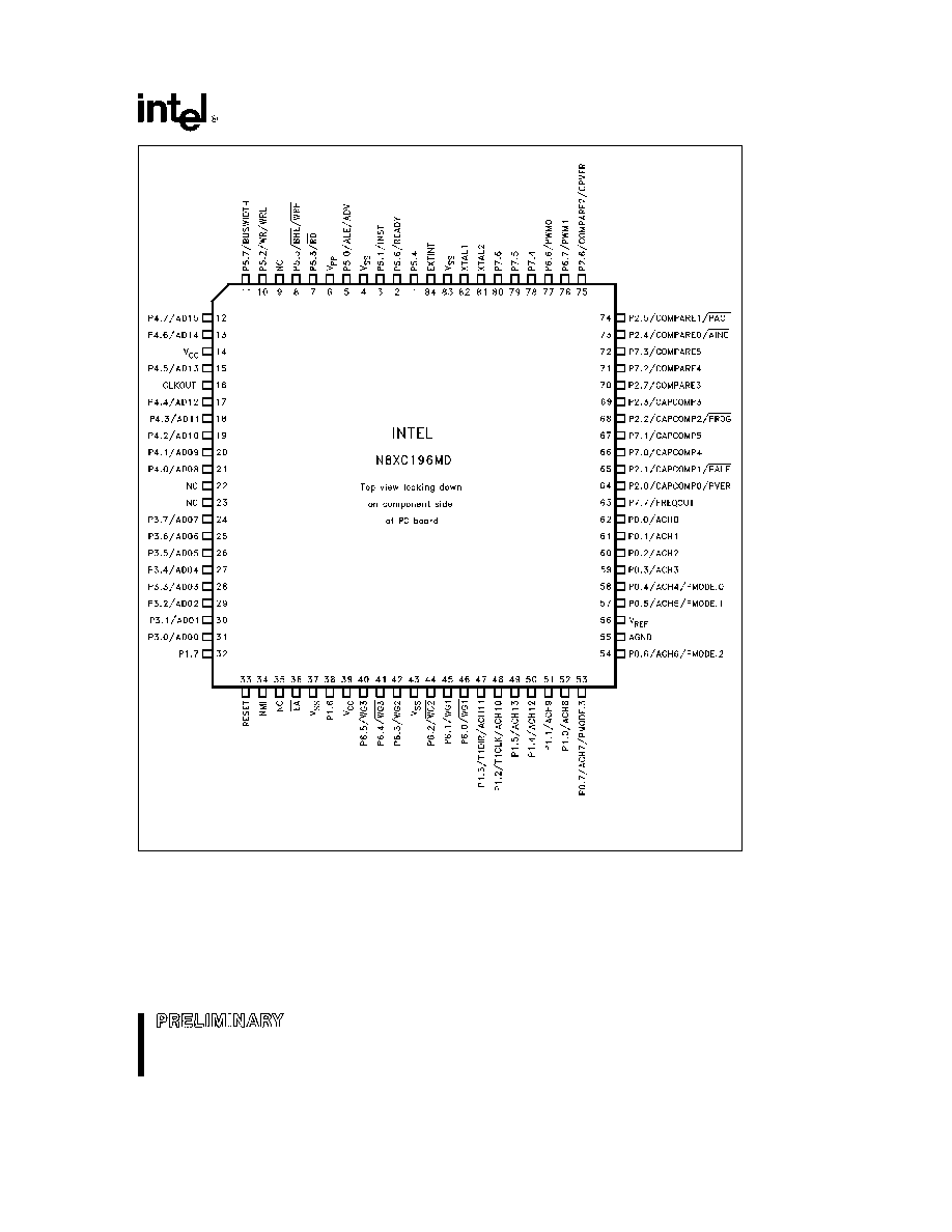
PIN DESCRIPTIONS
(Alphabetically Ordered)
Symbol
Function
ACH0 ≠ ACH13
Analog inputs to the on-chip A D converter ACH0 ≠ 7 share the input pins
with P0 0 ≠ 7 and ACH8 ≠ 13 share pins with P1 0 ≠ 5 If the A D is not used
(P0 0 ≠ P0 7 P1 0 ≠ P1 5)
the port pins can be used as standard input ports
ANGND
Reference ground for the A D converter Must be held at nominally the
same potential as V
SS
ALE ADV(P5 0)
Address Latch Enable or Address Valid output as selected by CCR Both
options allow a latch to demultiplex the address data bus on the signal's
falling edge When the pin is ADV it goes inactive (high) at the end of the
bus cycle ALE ADV is active only during external memory accesses Can be
used as standard I O when not used as ALE ADV
BHE WRH (P5 5)
Byte High Enable or Write High output as selected by the CCR BHE will go
low for external writes to the high byte of the data bus WRH will go low for
external writes where an odd byte is being written BHE WRH is activated
only during external memory writes
BUSWIDTH (P5 7)
Input for bus width selection If CCR bits 1 and 2 e 1 this pin dynamically
controls the bus width of the bus cycle in progress If BUSWIDTH is low an
8-bit cycle occurs If it is high a 16-bit cycle occurs This pin can be used as
standard I O when not used as BUSWIDTH
CAPCOMP0 ≠ CAPCOMP5
The EPA Capture Compare pins CAPCOMP0 ≠ 3 share the pins with
P2 0 ≠ P2 3 CAPCOMP4 ≠ 5 share the pins with P7 0 ≠ P7 1 If not used for the
(P2 0 ≠ P2 3 P7 0 ≠ P7 1)
EPA they can be configured as standard I O pins
CLKOUT
Output of the internal clock generator The frequency is
of the oscillator
frequency It has a 50% duty cycle
COMPARE0 ≠ COMPARE5
The EPA Compare pins COMPARE0 ≠ 3 share the pins with P2 4 ≠ P2 7
COMPARE4 ≠ 5 share the pins with P7 2 ≠ P7 3 If not used for the EPA they
(P2 4 ≠ P2 7 P7 2 ≠ P7 3)
can be configured as standard I O pins
EA
External Access enable pin EA e 0 causes all memory accesses to be
external to the chip EA e 1 causes memory accesses from location 2000H
to 5FFFH to be from the on-chip OTPROM ROM EA e 12 5V causes
execution to begin in the programming mode EA is latched at reset
EXTINT
A programmable input on this pin causes a maskable interrupt vector
through memory location 203CH The input may be selected to be a
positive negative edge or a high low level using WG
PROTECT (1FCEH)
FREQOUT
Programmable frequency output pin The frequency can vary from 4 KHz to 1
MHz (16 MHz input clock) It has a 50% duty cycle Pin may be configured as
standard I O if FREQOUT is not used
INST (P5 1)
INST is high during the instruction fetch from the external memory and
throughout the bus cycle It is low otherwise This pin can be configured as
standard I O if not used as INST
NMI
A positive transition on this pin causes a non-maskable interrupt which
vectors to memory location 203EH If not used it should be tied to V
SS
May
be used by Intel Evaluation boards
PORT0
8-bit high impedance input-only port Also used as A D converter inputs
Port0 pins should not be left floating These pins also used to select
programming modes in the OTPROM devices
PORT1
8-bit high impedance input-only port P1 0 ≠ P1 5 are also used as A D
converter inputs In addition P1 2 and P1 3 can be used as Timer 1 clock
input and direction select respectively P1 6 ≠ P1 7 can be used as input-only
pins
9
8XC196MD
PIN DESCRIPTIONS
(Alphabetically Ordered) (Continued)
Symbol
Function
PORT2
8-bit bidirectional I O port All of the Port2 pins are shared with the EPA I O
pins (CAPCOMP0 ≠ 3 and COMPARE0 ≠ 3)
PORT3
8-bit bidirectional I O ports with open drain outputs These pins are shared
with the multiplexed address data bus which uses strong internal pullups
PORT4
PORT5
8-bit bidirectional I O port 7 of the pins are shared with bus control signals
(ALE INST WR RD BHE READY BUSWIDTH) Can be used as standard
I O
PORT6
8-bit output port P6 6 and P6 7 output PWM the others are used as the Wave
Form Generator outputs Can be used as standard output ports
PORT7
8-bit bidirectional I O port P7 0 ≠ P7 3 can be used as EPA I O pins
(CAPCOMP4 ≠ 5 and COMPARE4 ≠ 5) P7 7 can be used as FREQOUT output
pin P7 4 ≠ P7 6 are standard I O pins
PWM0 PWM1
Programmable duty cycle Programmable frequency Pulse Width Modulator
pins The duty cycle has a resolution of 256 steps and the frequency can vary
(P6 6 P6 7)
from 122 Hz to 31 KHz (16 MHz input clock) Pins may be configured as
standard output if PWM is not used
RD (P5 3)
Read signal output to external memory RD is low only during external memory
reads Can be used as standard I O when not used as RD
READY (P5 6)
Ready input to lengthen external memory cycles If READY e 0 the memory
controller inserts wait states until the next positive transition of CLKOUT
occurs with READY e 1 Can be used as standard I O when not used as
READY
RESET
Reset input to and open-drain output from the chip Held low for at least 16
state times to reset the chip Input high for normal operation RESET has an
Ohmic internal pullup resistor
T1CLK
Timer 1 Clock input This pin has two other alternate functions ACH10 and
P1 2
(P1 2)
T1DIR
Timer 1 Direction input This pin has two other alternate functions ACH11 and
P1 3
(P1 3)
V
PP
The programming voltage is applied to this pin It is also the timing pin for the
return from Power Down circuit Connect this pin with a 1 mF capacitor to V
SS
and a 1 MX resistor to V
CC
If the Power Down feature is not used connect
the pin to V
CC
WG1 ≠ WG3 WG1 ≠ WG3
3 phase output signals and their complements used in motor control
applications The pins can also be configured as standard output pins
(P6 0 ≠ P6 5)
WR WRL (P5 2)
Write and Write Low output to external memory WR will go low every external
write WRL will go low only for external writes to an even byte Can be used as
standard I O when not used as WR WRL
XTAL1
Input of the oscillator inverter and the internal clock generator This pin should
be used when using an external clock source
XTAL2
Output of the oscillator inverter
PMODE
Determines the EPROM programming mode
(P0 4 ≠ 7)
PACT
A low signal in Auto Programming mode indicates that programming is in
process A high signal indicates programming is complete
(P2 5)
10

8XC196MD
PIN DESCRIPTIONS
(Alphabetically Ordered) (Continued)
Symbol
Function
PALE
A falling edge in Slave Programming Mode and Auto Configuration Byte
Programming Mode indicates that ports 3 and 4 contain valid programming
(P2 1)
address command information (input to slave)
PROG
A falling edge in Slave Programming Mode begins programming A rising edge
ends programming
(P2 2)
PVER
A high signal in Slave Programming Mode and Auto Configuration Byte
Programming Mode indicates the byte programmed correctly
(P2 0)
CPVER
Cumulative Program Verification Pin is high if all locations since entering a
programming mode have programmed correctly
(P2 6)
AINC
Auto Increment Active low input enables the auto increment mode Auto
increment will allow reading or writing of sequential EPROM locations without
(P2 4)
address transactions across the PBUS for each read or write
11

8XC196MD
ABSOLUTE MAXIMUM RATINGS
Ambient Temperature
Under Bias
b
40 C to a85 C
Storage Temperature
b
65 C to a150 C
Voltage from EA or V
PP
to V
SS
or ANGND
b
0 5V to a13 00V
Voltage on Any Other Pin
to V
SS
or ANGND
b
0 5V to a7 0V
(1)
Power Dissipation
1 5W
(2)
NOTES
1 This includes V
PP
and EA on ROM or CPU only devices
2 Power dissipation is based on package heat transfer lim-
itations not device power consumption
NOTICE This data sheet contains preliminary infor-
mation on new products in production The specifica-
tions are subject to change without notice Verify with
your local Intel Sales office that you have the latest
data sheet before finalizing a design
WARNING Stressing the device beyond the ``Absolute
Maximum Ratings'' may cause permanent damage
These are stress ratings only Operation beyond the
``Operating Conditions'' is not recommended and ex-
tended exposure beyond the ``Operating Conditions''
may affect device reliability
OPERATING CONDITIONS
Symbol
Description
Min
Max
Units
T
A
Ambient Temperature Under Bias
b
40
a
85
C
V
CC
Digital Supply Voltage
4 50
5 50
V
V
REF
Analog Supply Voltage
4 00
5 50
V
F
OSC
Oscillator Frequency
8
16
MHz
NOTE
ANGND and V
SS
should be nominally at the same potential Also V
SS
and V
SS1
must be at the same potential
DC ELECTRICAL CHARACTERISTICS
(Over Specified Operating Conditions)
Symbol
Parameter
Min
Max
Units
Test Conditions
V
IL
Input Low Voltage
b
0 5
0 3 V
CC
V
V
IH
Input High Voltage
0 7 V
CC
V
CC
a
0 5
V
V
OL
Output Low Voltage
0 3
V
I
OL
e
200 mA
Port 2 5 and 7 P6 6 P6 7
0 45
V
I
OL
e
3 2 mA
CLKOUT
1 5
V
I
OL
e
7 mA
V
OL1
Output Low Voltage on Port 3 4
1 0
V
I
OL
e
15 mA
V
OL2
Output Low Voltage on
0 45
V
I
OL
e
10 mA
Port 6 0 ≠ 6 5
V
OH
Output High Voltage
V
CC
b
0 3
V
I
OH
e b
200 mA
V
CC
b
0 7
V
I
OH
e b
3 2 mA
V
CC
b
1 5
V
I
OH
e b
7 mA
V
th
a
≠ V
th
b
Hysteresis Voltage Width on
0 2
V
Typical
RESET
12
8XC196MD
DC ELECTRICAL CHARACTERISTICS
(Over Specified Operating Conditions) (Continued)
Symbol
Parameter
Min Typ
Max
Units
Test Conditions
I
LI
Input Leakage Current on All Input
g
10
m
A
0V
k
V
IN
k
V
CC
≠ 0 3V (in RESET)
Only Pins
I
LI1
Input Leakage Current on Port0
g
3
m
A
0V
k
V
IN
k
V
REF
and Port1
I
IL
Input Low Current on BD Ports
b
70
m
A
V
IN
e
0 3 V
CC
(Note 1)
I
IL1
Input Low Current on P5 4 and
b
10
mA
0 2 V
CC
P2 6 during Reset (Note 3)
I
OH
Output High Current on P5 4 and
b
2
mA
0 7 V
CC
P2 6 during Reset (Note 4)
I
CC
Active Mode Current in Reset
50
70
mA
XTAL1 e 16 MHz
I
REF
A D Conversion Reference Current
2
5
mA
V
CC
e
V
PP
e
V
REF
e
5 5V
I
IDL
Idle Mode Current
15
30
mA
I
PD
Power-Down Mode Current
5
50
m
A
V
CC
e
V
PP
e
V
REF
e
5 5V
R
RST
RESET Pin Pullup Resistor
6k
65k
X
C
S
Pin Capacitance (Any Pin to V
SS
)
10
pF
F
TEST
e
1 0 MHz
NOTES
1 BD (Bidirectional ports) include
P2 0 ≠ P2 7 except P2 6
P3 0 ≠ P3 7
P4 0 ≠ P4 7
P5 0 ≠ P5 3
P5 5 ≠ P5 7
P7 0 ≠ P7 7
2 During normal (non-transient) conditions the following total current limits apply
P6 0 ≠ P6 5
I
OL
40 mA
I
OH
28 mA
P3
I
OL
90 mA
I
OH
42 mA
P4
I
OL
90 mA
I
OH
42 mA
P5 CLKOUT
I
OL
35 mA
I
OH
35 mA
P2 P6 6 P6 7 P7
I
OL
63 mA
I
OH
63 mA
3 Maximum current that must be sunk by external device to ensure test mode entry
4 Do not exceed minimum current or device may enter test mode
13

8XC196MD
EXPLANATION OF AC SYMBOLS
Each symbol is two pairs of letters prefixed by ``T'' for time The characters in a pair indicate a signal and its
condition respectively Symbols represent the time between the two signal condition points
Conditions
Signals
H
High
L
Low
V
Valid
X
No Longer Valid
Z
Floating
A
Address
B
BHE
C
CLKOUT
D
DATA
G
Buswidth
H
HOLD
HA
HLDA
L
ALE ADV
BR
BREQ
R
RD
W
WR WRH WRL
X
XTAL1
Y
READY
Q
Data Out
AC ELECTRICAL CHARACTERISTICS
(Over Specified Operating Conditions)
Test Conditions Capacitive load on all pins e 100 pF Rise and fall times e 10 ns F
OSC
e
16 MHz
The system must meet the following specifications to work with the 87C196MD
Symbol
Parameter
Min
Max
Units
Notes
F
XTAL
Frequency on XTAL1
8
16
MHz
3
T
OSC
1 F
XTAL
62 5
125
ns
T
AVYV
Address Valid to READY Setup
2 T
OSC
b
75
ns
T
LLYV
ALE Low to READY Setup
T
OSC
b
70
ns
4
T
YLYH
Not READY Time
No Upper Limit
ns
T
CLYX
READY Hold after CLKOUT Low
0
T
OSC
b
30
ns
1
T
LLYX
READY Hold after ALE Low
T
OSC
b
15
2 T
OSC
b
40
ns
1
T
AVGV
Address Valid to BUSWIDTH Setup
2 T
OSC
b
75
ns
T
LLGV
ALE Low to BUSWIDTH Setup
T
OSC
b
60
ns
4
T
CLGX
Buswidth Hold after CLKOUT Low
0
ns
T
AVDV
Address Valid to Input Data Valid
3 T
OSC
b
55
ns
2
T
RLDV
RD Active to Input Data Valid
T
OSC
b
22
ns
2
T
CLDV
CLKOUT Low to Input Data Valid
T
OSC
b
50
ns
T
RHDZ
End of RD to Input Data Float
T
OSC
ns
T
RXDX
Data Hold after RD Inactive
0
ns
NOTES
1 If Max is exceeded additional wait states will occur
2 If wait states are used add 2 T
OSC
N where N
e
number of wait states
3 Testing performed at 8 MHz However the device is static by design and will typically operate below 1 Hz
4 These timings are included for compatibility with older
b
90 and BH products They should not be used for newer high-
speed designs
14

8XC196MD
AC ELECTRICAL CHARACTERISTICS
(Continued)
Test Conditions Capacitive load on all pins e 100 pF Rise and fall times e 10 ns F
OSC
e
16 MHz
The 87C196MD will meet the following timing specifications
Symbol
Parameter
Min
Max
Units
Notes
T
XHCH
XTAL1 to CLKOUT High or Low
30
110
ns
T
CLCL
CLKOUT Cycle Time
2 T
OSC
ns
T
CHCL
CLKOUT High Period
T
OSC
b
10
T
OSC
a
15
ns
T
CLLH
CLKOUT Falling Edge to ALE Rising
b
5
15
ns
T
LLCH
ALE Falling Edge to CLKOUT Rising
b
20
15
ns
T
LHLH
ALE Cycle Time
4 T
OSC
ns
3
T
LHLL
ALE High Period
T
OSC
b
10
T
OSC
a
10
ns
T
AVLL
Address Setup to ALE Falling Edge
T
OSC
b
15
ns
T
LLAX
Address Hold after ALE Falling
T
OSC
b
40
ns
T
LLRL
ALE Falling Edge to RD Falling
T
OSC
b
30
ns
T
RLCL
RD Low to CLKOUT Falling Edge
4
30
ns
T
RLRH
RD Low Period
T
OSC
b
5
T
OSC
a
25
ns
3
T
RHLH
RD Rising Edge to ALE Rising Edge
T
OSC
T
OSC
a
25
ns
1
T
RLAZ
RD Low to Address Float
5
ns
T
LLWL
ALE Falling Edge to WR Falling
T
OSC
b
10
ns
T
CLWL
CLKOUT Low to WR Falling Edge
0
25
ns
T
QVWH
Data Stable to WR Rising Edge
T
OSC
b
23
ns
T
CHWH
CLKOUT High to WR Rising Edge
b
10
15
ns
T
WLWH
WR Low Period
T
OSC
b
30
ns
3
T
WHQX
Data Hold after WR Rising Edge
T
OSC
b
25
ns
T
WHLH
WR Rising Edge to ALE Rising Edge
T
OSC
b
10
T
OSC
a
15
ns
1
T
WHBX
BHE INST Hold after WR Rising
T
OSC
b
10
ns
T
WHAX
AD8 ≠ 15 Hold after WR Rising
T
OSC
b
30
ns
2
T
RHBX
BHE INST Hold after RD Rising
T
OSC
b
10
ns
T
RHAX
AD8 ≠ 15 Hold after RD Rising
T
OSC
b
30
ns
2
NOTES
1 Assuming back to back cycles
2 8-bit bus only
3 If wait states are used add 2 T
OSC
N where N
e
number of wait states
15

8XC196MD
SYSTEM BUS TIMINGS
272323 ≠ 5
16

8XC196MD
READY TIMINGS (One Wait State)
272323 ≠ 6
BUSWIDTH TIMINGS
272323 ≠ 7
17

8XC196MD
EXTERNAL CLOCK DRIVE
Symbol
Parameter
Min
Max
Units
1 T
XLXL
Oscillator Frequency
8
16 0
MHz
T
XLXL
Oscillator Period
62 5
125
ns
T
XHXX
High Time
22
ns
T
XLXX
Low Time
22
ns
T
XLXH
Rise Time
10
ns
T
XHXL
Fall Time
10
ns
EXTERNAL CRYSTAL CONNECTIONS
272323 ≠ 8
NOTE
Keep oscillator components close to chip and use
short direct traces to XTAL1 XTAL2 and V
SS
When
using crystals C1
e
20 pF C2
e
20 pF When using
ceramic resonators consult manufacturer for recom-
mended circuitry
EXTERNAL CLOCK CONNECTIONS
272323 ≠ 9
Required if TTL driver used
Not needed if CMOS driver is used
EXTERNAL CLOCK DRIVE WAVEFORMS
272323 ≠ 10
An external oscillator may encounter as much as a 100 pF load at XTAL1 when it starts-up This is due to
interaction between the amplifier and its feedback capacitance Once the external signal meets the V
IL
and
V
IH
specifications the capacitance will not exceed 20 pF
AC TESTING INPUT OUTPUT WAVEFORMS
272323 ≠ 11
AC Testing inputs are driven at 3 5V for a Logic ``1'' and 0 45V for
a Logic ``0'' Timing measurements are made at 2 0V for a Logic
``1'' and 0 8V for a Logic ``0''
FLOAT WAVEFORMS
272323 ≠ 12
For Timing Purposes a Port Pin is no Longer Floating when a
100 mV change from Load Voltage Occurs and Begins to Float
when a 100 mV change from the Loaded V
OH
V
OL
Level occurs
I
OL
I
OH
e
g
15 mA
18

8XC196MD
A TO D CHARACTERISTICS
The sample and conversion time of the A D convert-
er in the 8-bit or 10-bit modes is programmed by
loading a byte into the AD
TIME Special Function
Register This allows optimizing the A D operation
for specific applications The AD
TIME register is
functional for all possible values but the accuracy of
the A D converter is only guaranteed for the times
specificed in the operating conditions table
The value loaded into AD
TIME bits 5 6 7 deter-
mines the sample time T
SAM
and is calculated us-
ing the following formula
SAM e
(T
SAM
c
F
OSC
) b 2
8
T
SAM
e
Sample time ms
F
OSC
e
Processor frequency MHz
SAM e Value loaded into AD
TIME
bits 5 6 7
SAM must be in the range 1 through 7
The value loaded into AD
TIME bits 0 ≠ 5 deter-
mines the conversion time T
CONV
and is calculated
using the following formula
CONV e
(T
CONV
c
F
OSC
) b 3
2B
b
1
T
CONV
e
Conversion time ms
F
OSC
e
Processor frequency MHz
B e 8 for 8-bit conversion
B e 10 for 10-bit conversion
CONV e Value loaded into AD
TIME
bits 0 ≠ 5
CONV must be in the range 2 through 31
The converter is ratiometric so absolute accuracy is
dependent on the accuracy and stability of V
REF
V
REF
must be close to V
CC
since it supplies both the
resistor ladder and the analog portion of the convert-
er and input port pins There is also an AD
TEST
SFR that allows for conversion on ANGND and
V
REF
as well as adjusting the zero offset The abso-
lute error listed is WITHOUT doing any adjustments
A D CONVERTER SPECIFICATION
The specifications given assume adherence to the
operating conditions section of this data sheet Test-
ing is performed with V
REF
e
5 12V and 16 0 MHz
operating frequency After a conversion is started
the device is placed in the IDLE mode until the con-
version is complete
19

8XC196MD
10-BIT MODE A D OPERATING CONDITIONS
Symbol
Description
Min
Max
Units
T
A
Ambient Temperature
b
40
a
85
C
V
CC
Digital Supply Voltage
4 50
5 50
V
V
REF
Analog Supply Voltage
4 00
5 50
V
(1)
T
SAM
Sample Time
1 0
m
s
(2)
T
CONV
Conversion Time
10 0
20 0
m
s
(2)
F
OSC
Oscillator Frequency
8 0
16 0
MHz
NOTES
ANGND and V
SS
should nominally be at the same potential
1 V
REF
must be within 0 5V of V
CC
2 The value of AD
TIME is selected to meet these specifications
10-BIT MODE A D CHARACTERISTICS
(Over Specified Operating Conditions)
Parameter
Typical
(1)
Min
Max
Units
Resolution
1024
1024
Levels
10
10
Bits
Absolute Error
0
g
4
LSBs
Full Scale Error
0 25
g
0 5
LSBs
Zero Offset Error
0 25
g
0 5
LSBs
Non-Linearity
1 0
g
2 0
g
4
LSBs
Differential Non-Linearity
l
b
1
a
2
LSBs
Channel-to-Channel Matching
g
0 1
0
g
1 0
LSBs
Repeatability
g
0 25
0
LSBs
Temperature Coefficients
Offset
0 009
LSB C
Full Scale
0 009
LSB C
Differential Non-Linearity
0 009
LSB C
Off Isolation
b
60
dB
(2 3)
Feedthrough
b
60
dB
(2)
V
CC
Power Supply Rejection
b
60
dB
(2)
Input Series Resistance
750
2K
X
(4)
Voltage on Analog Input Pin
ANGND b 0 5
V
REF
a
0 5
V
(5 6)
Sampling Capacitor
3
pF
DC Input Leakage
g
1
0
g
3 0
m
A
NOTES
An ``LSB'' as used here has a value of approximately 5 mV (See Embedded Microcontrollers and Processors Handbook
for A D glossary of terms)
1 These values are expected for most parts at 25 C but are not tested or guaranteed
2 DC to 100 KHz
3 Multiplexer Break-Before-Make is guaranteed
4 Resistance from device pin through internal MUX to sample capacitor
5 These values may be exceeded if the pin current is limited to
g
2 mA
6 Applying voltages beyond these specifications will degrade the accuracy of other channels being converted
7 All conversions performed with processor in IDLE mode
20
8XC196MD
8-BIT MODE A D OPERATING CONDITIONS
Symbol
Description
Min
Max
Units
T
A
Ambient Temperature
b
40
a
85
C
V
CC
Digital Supply Voltage
4 50
5 50
V
V
REF
Analog Supply Voltage
4 00
5 50
V
(1)
T
SAM
Sample Time
1 0
m
s
(2)
T
CONV
Conversion Time
7 0
20 0
m
s
(2)
F
OSC
Oscillator Frequency
8 0
16 0
MHz
NOTES
ANGND and V
SS
should nominally be at the same potential
1 V
REF
must be within 0 5V of V
CC
2 The value of AD
TIME is selected to meet these specifications
8-BIT MODE A D CHARACTERISTICS
(Over the Above Operating Conditions)
Parameter
Typical
(1)
Min
Max
Units
Resolution
256
256
Level
8
8
Bits
Absolute Error
0
g
1
LSBs
Full Scale Error
g
0 5
LSBs
Zero Offset Error
g
0 5
LSBs
Non-Linearity
0
g
1
LSBs
Differential Non-Linearity
l
b
1
a
1
LSBs
Channel-to-Channel Matching
0
g
1 0
LSBs
Repeatability
g
0 25
LSBs
Temperature Coefficients
Offset
0 003
LSB C
Full Scale
0 003
LSB C
Differential Non-Linearity
0 003
LSB C
Off Isolation
b
60
dB
(2 3)
Feedthrough
b
60
dB
(2)
V
CC
Power Supply Rejection
b
60
dB
(2)
Input Series Resistance
750
2K
X
(4)
Voltage on Analog Input Pin
V
SS
b
0 5
V
REF
a
0 5
V
(5 6)
Sampling Capacitor
3
pF
DC Input Leakage
g
1
0
g
3 0
m
A
NOTES
An ``LSB'' as used here has a value of approximately 20 mV (See Embedded Microcontrollers and Processors Handbook
for A D glossary of terms)
1 These values are expected for most parts at 25 C but are not tested or guaranteed
2 DC to 100 KHz
3 Multiplexer Break-Before-Make is guaranteed
4 Resistance from device pin through internal MUX to sample capacitor
5 These values may be exceeded if the pin current is limited to
g
2 mA
6 Applying voltages beyond these specifications will degrade the accuracy of other channels being converted
7 All conversions performed with processor in IDLE mode
21

8XC196MD
EPROM SPECIFICATIONS
OPERATING CONDITIONS DURING PROGRAMMING
Symbol
Description
Min
Max
Units
T
A
Ambient Temperature during Programming
20
30
C
V
CC
Supply Voltage during Programming
4 5
5 5
V
(1)
V
REF
Reference Supply Voltage during Programming
4 5
5 5
V
(1)
V
PP
Programming Voltage
12 25
12 75
V
(2)
V
EA
EA Pin Voltage
12 25
12 75
V
(2)
F
OSC
Oscillator Frequency during Auto
6 0
8 0
MHz
and Slave Mode Programming
T
OSC
Oscillator Frequency during
6 0
12 0
MHz
Run-Time Programming
NOTES
1 V
CC
and V
REF
should nominally be at the same voltage during programming
2 V
PP
and V
EA
must never exceed the maximum specification or the device may be damaged
3 V
SS
and ANGND should nominally be at the same potential (0V)
4 Load capacitance during Auto and Slave Mode programming
e
150 pF
AC EPROM PROGRAMMING CHARACTERISTICS (SLAVE MODE)
Symbol
Parameter
Min
Max
Units
T
SHLL
Reset High to First PALE Low
1100
T
OSC
T
LLLH
PALE Pulse Width
50
T
OSC
T
AVLL
Address Setup Time
0
T
OSC
T
LLAX
Address Hold Time
100
T
OSC
T
PLDV
PROG Low to Word Dump Valid
50
T
OSC
T
PHDX
Word Dump Data Hold
50
T
OSC
T
DVPL
Data Setup Time
0
T
OSC
T
PLDX
Data Hold Time
400
T
OSC
T
PLPH
(1)
PROG Pulse Width
50
T
OSC
T
PHLL
PROG High to Next PALE Low
220
T
OSC
T
LHPL
PALE High to PROG Low
220
T
OSC
T
PHPL
PROG High to Next PROG Low
220
T
OSC
T
PHIL
PROG High to AINC Low
0
T
OSC
T
ILIH
AINC Pulse Width
240
T
OSC
T
ILVH
PVER Hold after AINC Low
50
T
OSC
T
ILPL
AINC Low to PROG Low
170
T
OSC
T
PHVL
PROG High to PVER Valid
220
T
OSC
NOTE
1 This specification is for the Word Dump Mode For programming pulses use the Modified Quick Pulse Algorithm
22

8XC196MD
DC EPROM PROGRAMMING CHARACTERISTICS
Symbol
Parameter
Min
Max
Units
I
PP
V
PP
Supply Current (When Programming)
100
mA
NOTE
Do not apply V
PP
until V
CC
is stable and within specifications and the oscillator clock has stabilized or the device may be
damaged
SLAVE PROGRAMMING MODE DATA PROGRAM MODE WITH SINGLE PROGRAM PULSE
2723231 ≠ 13
NOTE
P3 0 must be high (``1'')
23

8XC196MD
SLAVE PROGRAMMING MODE IN WORD DUMP WITH AUTO INCREMENT
272323 ≠ 14
NOTE
P3 0 must be low (``0'')
SLAVE PROGRAMMING MODE TIMING IN DATA PROGRAM
WITH REPEATED PROG PULSE AND AUTO INCREMENT
272323 ≠ 15
24

8XC196MD
87C196MD DESIGN
CONSIDERATIONS
When an indirect shift during divide occurs the upper
3 bits of the shift count are not masked completely
If the shift count register has the value 32
n where
n e 1 3 5 or 7 the operand will be shifted 32 times
This should have resulted in no shift taking place
8XC196MC to 8XC196MD Design
Considerations
8XC196MC and 8XC196MD are pin compatible
However there were several pins that were not con-
nected (NC) on the 8XC196MC that are I O pins on
the 8XC196MD Port 7 is a bidirectional port added
to the 8XC196MD Port 1 has one additional analog
or digital input that was connected to V
SS
on the
8XC196MC Port 1 also has two additional digital in-
puts See 8XC196MC and 8XC196MD Differences
Section of this data sheet
DATA SHEET REVISION HISTORY
This is the initial data sheet (272323-001) It is valid
for devices with a ``B'' at the end of the topside
tracking number Data sheets are changed as new
device information becomes available Verify with
your local Intel sales office that you have the latest
version before finalizing a design or ordering devic-
es
25