
IXF32003
10Gbps Section and Line Termination Device
Product Description
The Intel
Æ
IXF32003 is a transport termination
device designed for use in SDH STM-16/64
and SONET OC-48/192 optical communication
systems. The IXF32003 integrates all main
functions of a section and line terminating
transceiver including
s
STM-64/OC-192 deframing
s
Overhead extraction
s
Overhead manipulation
s
STM-64/OC-192 framing in a single monolithic
IC, directly interfacing to an external front-end
(e.g., GD16584/85), as required at line side
The device has a line side interface with
16 parallel 622Mbps LVDS inputs and 16 parallel
622Mbps LVDS outputs. The output stage
supports either forward or counter clocking.
At system side, the IXF32003 supports one
10Gbps data stream, or four 2.5Gbps data
streams, in both receive and transmit directions.
The system side interface consists of 16 parallel
622Mbps LVDS data inputs for the transmitter
section and 16 parallel 622Mbps LVDS data
outputs from the receiver section. Users can operate
the system interface in two different modes:
s
STM-64/OC-192 (10G) mode. Used for
connecting 10G path-terminating equipment.
In 10G mode, the 16 data lines are synchronous
to one clock. An integrated cross connect level
allows you to deliberately remap STS-1 streams
within the STM-64/OC-192.
s
Four-times STM-16/OC-48 (2.5G) mode.
Used for connecting the IXF32003 to four
2.5G path-terminating devices. In 2.5G mode,
the device builds four groups of four data
lines each, which are synchronous to four
separate group clocks.
The IXF32003 supports various types of
overhead processing. You can choose to mani-
pulate overhead via the processor interface, or
you can add and drop overhead via dedicated SOH
interfaces, which allows additional external over-
head processing. You can also choose to add and
drop the whole overhead of all STS-1 channels.
Intel manufactures the IXF32003 in a 0.18µ
CMOS technology, and delivers the device in
a 576-pin ball grid array (
TBGA) package. The
IXF32003's typical power dissipation is
approximately 3W.
Features
s
STM-64/OC-192 data processing
s
16-bit input and 16-bit output 622MHz LVDS
line side interface
s
Easy interfacing to the Intel
Æ
10Gbps chipset
GD16584/85
s
Event monitoring (LOS, LOF, OOF)
s
B1, B2, M1 extraction, monitoring, and
optional insertion and event sum-up over a
programmable time period
s
Optional SONET/SDH scrambling/descrambling
s
Signal Degrade and Signal Fail detection on
B2 errors
s
J0 capture and optional insertion over
16 (64) frames
s
Detection of section trace mismatch
s
K1/K2 byte observation for APS MS-AIS/RDI
detection and optional insertion
s
AU-AIS/CI detection and optional insertion
product brief
www.intel.com/
design/network
(continued)
Transmit OH Processing
Within the line side transmitter section, the device performs
optional overhead processing. Bytes may be inserted by the
host processor or via the serial interfaces. In addition, AIS
may be automatically inserted when the receiver detects LOF,
LOS, SD or SF (all triggering events are programmable).
The AU-AIS insertion can also be configured. Valid B1/B2
checksums are generated. With scrambling activated, an
OC-192/STM-64 signal is transmitted, compliant with ITU,
ANSI or Bellcore standards. The line side output is a synchronous
16-bit parallel 622Mbps LVDS interface. At the line interface,
the device transmits either unmodified original overhead data
(transparent mode) or the generated overhead data.
Loopback
The IXF32003 supports four loopback modes:
s
System-side loopback without overhead operation, and with
STS-1 rearranging possibility
s
System-side loopback with overhead operation and
OC-192/STM-64 framing/deframing, and with STS-1
rearranging possibility
s
Line-side loopback without overhead operation, and
without STS-1 rearranging possibility
s
System-side loopback with overhead operation and
OC-192/STM-64 framing/deframing, and with STS-1
rearranging possibility.
Intel
Æ
Internet Exchange
TM
Architecture:
A New Approach to Development
Intel
Æ
Internet Exchange
TM
Architecture (IXA) is an end-to-end
family of high-performance, flexible and scalable hardware
and software development building blocks designed to meet
the growing performance requirements of today's networks.
Based on programmable silicon and software building blocks,
Intel
Æ
IXA solutions, enable faster development, more cost-
effective deployment, and future upgradability of network
and communications systems. Additional information can
be found at www.intel.com/IXA
Applications
s
STM-64/OC-192 terminal equipment
s
STM-64/OC-192 switching systems
s
Transparent 10G transport via 2.5G
s
STM-64/OC-192 OTN interfaces
s
In-system concentrator
Overhead Interfaces
Once per frame, the whole overhead for the first STM-1
channel (the first three STS-1 channels, respectively) is
accessible via a serial 19MHz interface port. Additionally,
an 8-bit parallel 78MHz interface outputs the complete
overhead of all 64 STM-1 and 192 STS-1 channels, respec-
tively. The Order Wire bytes E1/E2 and the Data Communication
Channels D1-D3/D4-D12 are also accessible via dedicated
serial interfaces.
System Side Interfaces
The IXF32003 passes payload data to a cross connect matrix,
where you can optionally rearrange the positions of the STS-1.
The system side output interface consists of 16 parallel LVDS
signals at 622Mbps. You can configure them as all synchronous
to a single clock, or group them by four lines with a separate
clock per group. Optionally, the device can generate framed
and scrambled OC-48/STM-16 data with a recalculated B1
parity. You can use this data to connect the device to four
OC-48/STM-16 path-terminating devices. With external
De/Mux and CDR components, you can achieve this by using
connections at 2.5Gbps. At receiving system side, you can
input four STM-16/OC-48 devices, each having four data
lines at 622Mbps, a frame pulse and 622MHz clock input
and output. Intel recommends that the four 2.5Mbps sources
be synchronously clocked.
If the 2.5Mbps sources support the SONET/SDH frame
alignment and feature a descrambler, the device will recover
the frame start by itself and the frame pulse input is not
needed. The interleaver combines the received bytes of all
inputs into the proper order for STM-64/OC-192 processing.
Using the cross connect matrix, you can rearrange the
payload channels to any position in the STM-64/OC-192
with an STS-1 granularity. Alternately, the device supports
a 10G input via 16 synchronous input lines with an optional
frame strobe. This mode is especially suited to supporting
OC-192c applications.
Received OH Processing
The IXF32003 takes aligned data bytes for a complete frame to
calculate a BIP-8 checksum, which it then compares against
the next received B1 byte. The device supports Automatic
Protection Switching (APS) by automatically monitoring SOH
bytes K1 and K2. The least significant bits of K2 indicate
MS-AIS and MS-RDI events. The Synchronization Message
S1 and the User Channel F1 are stored and checked for
changes. The received J0 bytes are stored in a 64-byte cyclic
store that is readable by the host processor. The Section
Trace Mismatch evaluation is programmable to SDH or
SONET standards. Pointer bytes are checked for AU-AIS and
concatenation indication. B2 checksums are calculated and
monitored in the same manner as B1. In addition, an updated
M1 is generated and passed to the transmitter for remote error
indication. The monitoring section sums all events including
B1, B2 and M1 error counts over a programmable time
period. The results are readable by the host processor. You
can configure both elapsed time period count and APS event
to generate processor interrupts.
Features
(continued)
s
F1, S1 observation and optional insertion
s
Periodical-driven host events
s
8-bit host processor interface with interrupt logic
s
SOH extraction/insertion via processor registers
s
Serial or parallel interface for SOH extraction and
optional insertion
s
Dedicated serial extraction and insertion interfaces for
E1/E2 and D1-D3, D4-D12
s
Terminal side interface capable of multiplexing/demultiplexing
s
4 x 2.5Gbps data
s
Frame regeneration at terminal side for 2.5Gbps data
s
10G terminal interface for OC-192c
s
Phase alignment FIFO for incoming four 2.5Gbps data
streams on system side compensating up to 500 ns skew
s
Full cross connect capability at STS-1/AU-3 level
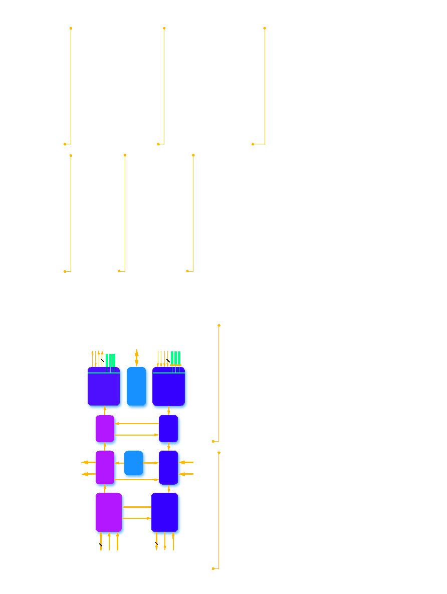
Serial
Interfaces
SOH
Access
16
16
Loopback
Loopback
LDIN
LICI
LD_LOS
SOCO1
SOCI1
SOFP1
SDOUT(3:0)
LDOUT
LOCO
LOCI
SDH/SONET
STM-64/OC-192
Deframer
OOF/LOF
OH Generation
OH Extract
STS-1
Cross
Connect
4 x 2.5G
DeMux/
Interleaver
4 x 2.5G
Mux/FIFO/
Interleaver
Processor
Interface
8-bit
Interface
Serial
Interfaces
SOH
Access
STS-1
Cross
Connect
OHC RAM
SDH/SONET
STM-64/OC-192
Framer
4
2
3
4
SICI1
SD_LOS1
SIFP1
SDIN (3:0)
2
3
4
4
IXF32003 Block Diagram